Note: Descriptions are shown in the official language in which they were submitted.
CA 02218706 1997-10-20
W 096/3299~ PCTnUS96/05422
GAMEPORT COMMUNICATION APPARATUS AND METHOD
The present invention relates to the use of a g~ll~OIl in c~ ....~e~ with a eo.~ t. -, and in
5 particular to a method and ~Jpalcllu~ for use in u-- .j- ~~ . with ga~llel~ul b in~ ln~ing those typically
cullrl~;ul~d for a personal c-....l.ut~ - (PC) such as an IBM PC~ or M~ G CullllJut~,,.
BACKGROUND INFORMATION
Many cr.. l.. -t~ - ~ sueh as an IBM PC~), XT, AT, 386 andlor 486 (or cu~ JaLal)le) COIll~ u~l or
a I~ 1.~ c- ~- . .l ~ut~ are provided or l ~ LI urlu~,d with a galll~ul L Various ~ dal ~ls for ~,alll~ ~JUI b
have been used. A eommon standard is that dci.~,lil,ed in TRM TP~hni~l Reference. Optio~c ~nd
Ad~fPrs, Vol. 2 "IBM Game Control Adapter" No. 6361493 (1986) - available as part ofthe IBM
Personal Computer Hardware Referenee Library and illCol~Jul. t~,d herein by l~,rc.~,uce. In one
15 collrlgu...Xon, a ~;alll~ol ~ provides between four and eight c~ .. . " " ""ir i.~ ion lines (along with various
voltage or ground lines). According to the standard, at least two, and up to four, lines are coupled to
variable resistors in one or more external deviees, sueh as the type of variable resistors found in a
typieal joystiek input deviee. Typieally, a joystiek permits c~ l i- - . of two variable resistors to two
of the lines, and one to four button or trigger signals over one to four of the 1-, . . -;. . ;. .g Iines. A second
20 joystick may provide for eoupling of first and seeond variable resistors through two ~rlr1ition~1 lines.
In previous deviees, the use that eould be made of the ~;alllc~Jul b was limited beeause systems
were typically collrl~;ul~,d to connect a ...-- ~ ;.... ~- .. of four axes and a total of four buttons. Although
sueh systems can be used for many purposes, ;",-I."l;"g playing many eurrently-available games on
co-.~l-ut~ :., beeause of the way the systems were collrl~;ul~d and used in the past, the limit~ti~ n on the
25 number of joystieks that can be attached, the number of buttons that ean be used, and the effeetive rate
at whieh illrul Illa~ion is input from the joystieks to the CC Ill,~luL~., previous systems have l ~ 1 ie~;d the
use that ean be made of the ~;alllc~Jol ~. These restrietions are particularly apparent for more reeent
generations of CullllJut~,. . which have a capability of ~IU-~C;~illg inrullllaLiull at rates which are much
higher than rates at whieh ;. . r( ~- I . ~ -1 ;~ ~- ~ is provided through the galll~,lJUI l aceording to previous
30 systems. Many previous uses of the ~;CLUIC~JUI t required disabling of illL~ .l u~t~ in order to service the
g~ JUI l. ~ litinn~lly, previous systems typieally required ~JIUglallllll~ -~ to make frequent inquiries
to detPnninP the eurrent e~n~liti~m of the joystieks attaehed to the ~,al~ Jul ~. This plaeed an
ulldc~ilable ~lu~;l~llllling burden on game d~ lop~-~. Previous uses of g~llcpolb often resulted in an
ulldc~ilably high amount of overhead (i.e., the amount of CPU time whieh is devoted to polling or
35 otherwise servieing the joystieks via the galll~)UI~) partieularly if the pi~Oglallllllillg using the ~;~LIIICIJU
was not carefully written. In many cases, the difficulty and complexity of ~lu~,lalllllling for previous
uses of a ~;alllcpul ~ led to ~lu~ullllling errors or software tliffl- ulti~ leading to calls or inquiries for
technical support.
CA 02218706 1997-10-20
W O 96132995 PCTnUS96/05422
In at least some previous uses of g~UIIC~JUl 15~ during the periods of time the ~ alllepul I was
being polled or U~ ,l wise serviced it was illrta~il,lc for the c-....l.ulr, to perform other tasks, effectively
monopolizing the cc ~ t~ - for relatively long periods; a situation which may not be tolerated by some
o~ dtillg systems (such as IBM~ OS/2) or user ill~-ra-,es (as A~ d for Miwuson~ Windows
5 95).
It would not, in general, be desirable to completely redesign the ~;aullc~JulL interface
~e~.; r;.,AI ;- .. .~ because of the uuld~,;,iual~;lity of rendering hlu~ a~ive or obsolete the existing base of
joysticks or other I/O devices, ~alu~ ul I cards or multi-I/O cards, and/or software, all of which, to a
greater or lesser extent, are cvurl~;ulGd to operate in accûldallcG with a standard galllL~ull ~l-e-;lAAAl;--1),
10 similar to that described above.
Accc ldiu~,ly, it would be ad~ ge( u~ to provide a method and alJI~aua~u~ for use with a
y,~llllCI~UI L which permits connection of a larger number of joysticks or other devices, provides for a
higher rate of ;..r(- .- A1;-~,1 transfer, preferably ~. A;-~IA;-~;~ E cc, ~ ;hility with previous gs~ .oll~
and/or ~UII~IJUI I cards or multiple-I/O cards and/or, with previous joystick devices and/or previous
15 sofLware. It would be ad~,A-.IS~ero--~ to provide a system which reduces I~lO~5lallllllCl burden, is low
cost and takes advantage of the iul~,l..ased speed and power of current and al-li.,i,....~d future culll~ ~.
SUMMARY OF THE INVENTION
The present hl~ iun includes a l~.CGg~ of the l~ul;l~.us found in previous devices. One
of the ~iffiAI~hi~ss of previous a~ ua~hcs has been the design of systems for providing in rl-. ~
flow through the ?~alll~pol~ in one direction only, i.e., from the joystick or other p~.lilJhc.àl device to the
C~ ut~ . The present invention includes c-- ~ ~ e ;--r~-....A1;- m or signals from the COIllyut~,. to
an external device through a g~ JUI L In one ~ ~ . .ho l ;. . . ~1 signals on one or more of the galll~,~JUI l
25 lines are used by an external device to generate timing or other signals e.g., for use in controlling the
flow of i. . ru~ n to the c- " "I" ~ .
Another difficulty with previous devices related to providing iurullll iun ~~ig~udiug the
position of a joystick in analog form. According to one embodil--~ nl of the present invention,
;~ ~ rU~ about the position of a joystick is l~_laÇ~ ,;i to the c- ~- ~ ~ via a ~alll~,pul I in digital
30 form. In this way, a larger amount of i..ru...l- tioll can be ~lall;,l~ d per unit time (e.g., to
a~.c.. odA1~ a larger number of joysticks, to provide more detailed or finer movement discrimination,
to provide a~ AI input such as inputs from p~ iti-)nAI buttons or triggers, and the like).
According to one eTnl~o~l ;- ~ ~- - ~l of the invention, inru----alion from a p~ . ipl-~. al device such as
a joystick, which may include proportional or analog hlr .. .~ .. ., is -lieiti7~l, e.g., to indicate the
35 position of a joystick and/or a~,~ivaliun of one or more joystick buttons, and/or to identify the type of
joystick or other device. When it is desired to obtain information about the position or status of the
joystick, the c-,...l~t ~ issues a signal, causing the voltage on one of the gameport lines to change (e.g.,
to begin iUl~ a.~lllg). Apparatus coupled to the ~, lle~JUI I senses this change, and 6~,.lc...,~ ;. signals,
CA 02218706 1997-10-20
W 096/32~95 PCTr~'9GJ~5422
e.g., timing signals, whieh are used to transfer the digitized and stored data through the gameport,
pl~,f~,.al~ly over one of the other ~;alll~JUl l lines. In one c.llbodilll~,.ll, the "trigger" signal is provided
on the X-axis, joystiek A line, and the digitized data is provided over one or more of the buKon lines.
In one embod--lsc.lL, four joystieks ean be used and the digitized data from the four joysticks is
G 5 provided over ~~,;",c~ , ones of the four button lines of the ~ ;ipUl 1. In one emho~lim~ nt the digital
data is output from the external deviee in s~ ,lllu~lu~i, serial fashion.
Aeeording to one r~n~ho.l;...-...l, the external ~ uaLua whieh is coupled to the ga~ JulL can
be readily cu--r~ul~,d to aeeept data from a standard (analog) joystiek, sueh as by providing a switeh
whieh eouples a standard joystiek to the ~ JUl I in the standard fashion.
BRIEF DESCRIPTION OF THE DRAWINGS
Fig. I is a block diagram of a typieal personal c-~ .u - system;
Fig. 2 is a bloek diagram showing e-.. -.i~ n lines eoupling two joystieks to a Cr~ t~ -
15 via a ~ ulL acculdi,lg to previous deviees;
Fig. 3A is a bloek diagram ~' r ~ ' ~ g eoupling of a four-buKon joystiek to a c~ l-ut~ - via a
g&ll~JUI I accollulg to previous deviees;
Fig. 3B is a bloek diagram d~,"- g eoupling of a two-button joystiek to a CUIIIIJU~ via a
~, ll~ull accul-lillg to previous deviees;
Fig. 4 is a s~ diagram of the e~ui~al~lll eireuitry for a joystiek eoupled to a game
eontroller accol.lillg to previous deviees;
Fig. 5 is a timing diagram of signals of a type provided in c~ .. with the eireuitry of Fig.
4;
Fig. 6 is a bloek diagram ~' r ~ ' ~ g eoupling of four joystieks to a U~ 'UI ~ ~ via a g~ UI
25 using an ~YI.,-:- box, accul.lhlg to an c-ho.l;l .l of the present invention;Fig. 7 is a sr l .~ l ;r diagram of an equivalent eireuit for providing load and eloek signals, as
shown in l;ig. 6;
Fig. 8A is a timing diagram showing the relative timing of signals accor Ihlg to the
,-.... ..... ..ho-l;~--- ~-~ of Figs. 6 and 7;
3û Fig. 8B is a bloek diagram of shift register and eoupled eireuitry;
Fig. 9 is a bloek diagrarn showing eoupling of four joystiek deviees to a C(JIII~U~. via a
g_,lc~olL, using an ~ box, accc,..lh.g to an embodiment of the present i-.~,..Lioll;
Fig. 10 is a bloek diagram dcpi~,lillg mode ~ ,hillg for various types of joystieks, accul.lhlg
to an ~ ~..l~o.l;...- -l ofthe present invention;
35 Fig. 11 is a nu.. ~ L of a ~JlU~Cdul~ according to an embodiment of the present invention;
Fig. 12 depiets data storage in registers aecording to an embodiment of the present hl~ CllliUII;
and
Fig. 13 is a flowehart of a l -u~6duu~i acculdu.g to an emho~l;...l -.1 of the present invention.
CA 02218706 1997-10-20
W 096/32995 PCTrUS96/05422
DETAILED DESCRIPTION OF THE PREFERRED EMBODIMENT
Before dca~fll,.llg methods and ..~.~, ~u~ according to the present invention, a short
5 des~ ,liu.. of a c~ t~ system that can be used in c~ with embodiul.~.lb of the present
invention will be provided.
Fig. I depicts cuu-pv--~"-b of a c-.~..l.ut~ ~ system generally of the type known as a 486
cv...~ t~ .. . As shown in Fig. 1, the cv-..~ system includes a mi~.ulJlv~ vr 102 coupled to a
plurality of controllers and p~ .llc,als, which are optional, d~p~n~iing on the system configuration.
10 The mic~u~ucc~ ~ul includes a bus interface 104 for i--~.ra~,i.-g with, e.g., mass storage units and
p~ Jh~lals. An address driver 104a provides proper addresses on the address bus of the proper level
for storing and tr~ncmitting ;..r~ - ... ;0.. inc~ ling program ;..rl.. ",~ n and data to and from a
cu..~ io.lal memory, such as dynamic random access memory (DRAM) 108, e.g., via a DRAM
controller 108b or a direct memory access (DMA) controller 108b, or to and from a hard drive 110, via
15 a hard drive controller 110a or a floppy drive 112 via a floppy drive con~roller 112a, or to or from
network storage over a local area network (LAN) 114 via a network controller 114a or to or from other
data sources and sinks such as remote devices, e.g., via a modem (optional), e.g., for Internet access or
C.J~ C with other network systems. a mouse or keyboard 122, via keyboard interface 120, or
a joystick 123a via a joystick or game eard or controller 123b.
Traffic on the bus is controlled using, e.g., a bus control request se~ 'f~ 104b, a bus burst
controller 104c, and a bus width controller 104d. Accuracy of c-.. -~-~i~ ;~,~- is checked usimg a
parity g~lC d~Ul and controller 104e. A cache memory 116 controlled by a cache unit 116a and
cu.. ~-.;- - ;-.g via a cache controller 116b provides for wait-state-free access to conventional memory
108. The cache memory 116 is smaller than CO~ iulldl memory 108 but has much shorter access
25 time. It is controlled in such a way as to be likely to contain the i.. rv.... ~ which will be needed by
the pluceaaol on a relatively short time frame. The mixed instruction and data cache 116 provides a
buffered write-through to ensure data in the coll~ lliollàl memory is current. Transfer of data to and
from the cache memory occurs in burst mode using the burst controller 104C.
The bus 103 consists of a control bus 105, an address bus 106, and a data bus 107. Illt~,~lulJ~a
30 from external devices are controlled by an interrupt controller 118 and passed to the mi--o,~,.v.,~a~ùl
102. A keyboard interface or controller evaluates user input received from the keyboard or other input
units, such as a mouse, pen and the like, and issues a cu--~ ~l.ol--l;..g signal to the keyboard interrupt of
the C~.."~ t~ - . The keyboard controller receives serial data from the keyboard cable and stores the data
~.lllJula.;ly for delivering them to the CPU 102. A timer 124 g. ~~ 5 timing signals for the interrupt
35 controller 118 and the system clock.
In order to provide access to a large range of memory locations, program hlall u-,lio..s
typically employ logical addl ~aSCS. In order to access the correct memory location, either from the
cache 116 or, if n~,ccsaa.y, by retrieval from conventional memory 108, it is necessary to convert the
CA 02218706 1997-10-20
WO 96/32995 PCT/US96/05422
logical address into a physical address. In the depicted embodilllc.lL, a word has a logical address with
three c~ a segment address, a page address, and a ~liD~ ~1 address. A segment table
130 contains, for each segment, a pointer to the base of the cull~ ng page table. The page table
132 is a memory map which, for each logical page address, contains a cullr ~ ..l;,,g physical address
5 of a page in main or secul.daly memorv. To speed up the address LIA ~ ;0~ process, part of the
memory map is replaced by a high speed memory, the ll allalaLion lOf~ C;~Ie buffer (TLB) 134. A
logical address is, thus, lli.. 'r(.. Pd by the segment table 130 and page table 132 or TLB 134 into a
physical address for h~ n over the physical address bus 136 to the cache.
In order to assure that the CPU 138 (;..~ l;.,g a barrel shifter, a status register and an
10 ~;LLIl_Li~/logic unit (ALU)) can receive a constant stream of hl ~u~,~iulls~ an hl:.LIu~,~ioll or c~mmS~ncl
memory 140 is provided, cdupled to a pre-fetcher 14Z for fetching the next iulaLI UCLiùll for the queue.
Comm~n~lc from the queue are provided to a c~mmi~n~l decoder 146 which decodes the macro
iuaLIu~,LiOlls to provide decoded instructions or micro hlaLI u-,LiGIls. A control and ~IVt~ _ti~ _ unit,
;,,g a control read only memory (ROM) 148 provides control signals to control flow of data and
15 hlaLIu~,Liulla to the CPU 138. When an hlsLIu-,Lioll requires floating point ~uiLlull_t;c, the instruction is
provided to a math CO-~JIu~,C.-~vl unit or floating point unit (FPU) 150.
Graphic output is dialJla~_d on a c~ - screen or monitor 152, such as a VGA or SVGA
monitor via a graphics card 154. Read only memory, such as erasable ~IU~ ble read only
memory (~PROM) device lS6 is used for storing nullvuldtile and/or p- - ...~ lu~allllllcd
2û i.. r,.. ,.~ ,. Typically,fora486cc.. 1.ut~ ,asetofillaLIu~ sfor(,lga.li~iulgbasic rl~r~ csuchas
acc~ p_.;~l~clal devices and mass storage, initial boot-up of the c-....l~u~ ~ and the like, such as that
known as the basic ill~,uL/uu~l,u~ system (BIOS) is stored on read only memory device 156. ~lflition~
system iul:~LI u-,Liulls, such as a disk operating system (DOS), e.g. Mi~,l uaun~ DOS 6.2 are stored
typically on the hard disk 110 or floppy disk drive 112. ~ ition~lly, in a typical system, a user
25 interface such as a graphical interface like Mi.lùsun6) Windows is stored on the hard drive 110.
Commnni~ti~n among the p~ al units over a local bus 162 is controlled by local bus controller
164.
Application ~JIU~,IalllS typically can be stored on the hard drive 110 or a floppy disk 112 and
work in coop- -~ with the BIOS and system program, such as DOS, e.g. for I a--sr_.lhlg data and
30 instructions to and from the hard drive 110 to the cûn~.lLiullal memory 108, cache memory 116 and/or
CPU 138. Preferably, the applic_;iull program works in cooperation with the user interface program
such as Mi-,luaun~ Windows for controlling display of output on the monitor 152, e.g. in full screen
mode or whldu.._d mode, multi-tasking the application program with other cu,.,~ " u~_.a~iOilS
and/or receiving user input, e.g. via the keyboard, mouse, etc. 122 and ll; l~ ;llg the input to the
35 CPU for controlling operation of the ~JIicdtiull program.
There are several ways in which the c~ ul may co~ lr with external or p~liyhc.al
devices. One method of co........... -~ tir~n involves issuing from the main micluproces~ùl an escape
c~mm~n~l (e.g., for sending certain hlrull--~iu-l to a printer). A second metnod involves sending
CA 02218706 1997-10-20
W 096/32995 PCTrUS96/05422
i..r~ ... to a memory which can be accessed by p~ c.al devices. A third method involves
c- .~.. ;. -1 ;on to and from a port. When data is to be obtained from an external device via a port, the
cu~ .ut~.. will place any necessary cu~ on the commAn~i bus, and place the port address on the
address bus. Thus, the various port ad~L ~.,a~S OCCUpy a certain amount of the address space of the
c~..... l.ut~ .. A ~JlU~allllllcl may retrieve data from a port by using assembly language cu.. - ,-ic
and/or by invoking various basic input/output system (BIOS) fimctiong e.g., by issuing c-........ .-A-~-1c in a
higher-level ~.u~a..l",ing language such as C or Basic.
By cc,,.~ iull, the address assigned to the ~alllcl~ull is 0201h. In order to connect an external
device such as a joystick to the y,a...c~,u. L, e g., for providing c- ~ A1 inn from the joystick via the
10 g~c~ulL to the c-~..l-u~, in addition to a ~ e a logical address to the ga.,,L,~,u,L, it is also
necessary to provide physical devices for achieving the cn....r~ liu . The physical devices typically
include a plug, such as a female D 15 standard plug, and interface circuitry. The interface circuitry or
adapter performs a number of fimrtinnc inr~ ine ~~,co~,. . ;, ;. e the ~;alll~ ~JUl I address when it is placed
on the address bus, responding to a commAn~l such as a write commAn~i or read cnmmAn~l while the
15 ~ ,o,l address is asserted, such as by closing one or more logical switches (as described more fully
below), cnn~litinnine various signals (e.g., to provide logical signals at the correct voltage for placing
on the data bus), and controlling timing of various U~ aliUll5, as dc.,~" il,cd more fully below. In some
cases, the plug and the interface circuitry are placed on an ~ - .. board for inctAll~tinn in the
chassis of the c- ....l.- ~t- ~ in the normal fashion. One type of such board is a "~; ".,I-u~ ~ card," designed
20 ~ uai~_ly forc-~ ~ e joysticks. Some"soundcard"~ c:-~..cardsincludeagall.,~ull. Another
type of card is a multiple-I/O card, which typically includes, in addition to the ga ll~ ~Ul I plug and
ACCOI ~ interface circuitry, several other i..~,.raccs such as a parallel interface and one or more serial
illt~,~ra.~cs~ with r~ plugs (or "jacks"). In some c-....l-u'~ - ~ the plug and interface circuitry
making up the gall~ Jull are built into the c~----l- -~- -, rather than being located on an ~qYpArle;~n board.
25 There are typically two general modes of cu-""~ Atine with the mi.. -u~Jlucessul~ polling
and interrupt. In a polling system, the mi~i~ulJ~ucessol issues cnmmAn~lC at times det~rmin~d by a
cn-..l.-~t~ ~ program, for l-~l--- o;~e data from an external device. In an interrupt system, an external
device can issue an interrupt signal 115a to an interrupt controller 115b. At an alJlJlulJlialt~ time, the
interrupt controller 115b provides an interrupt signal onto the bus 103 which is eventually l-,cog"i~d
30 by the miclo~-,ùc.~au~, which then suspends or illL~ll u~b the normal ~luCC~aillg~ and executes an
interrupt handler routine. In most cases, data through the ~;,alUclJUl l is handled using a polling
~ucedul~. In a few cases, ~ cl)u~l data is handled by an interrupt l~ucclu-~, such as by making use
of a software BIOS call to 0015h.
Most joysticks used in conn~oction with desktop c- ~. . .l .ut~ are either a switch type or an
35 analog type. An analog (or "proportional~') joystick provides information regarding the amount of
d~ fl~ctinn of the joystick in left-right, and/or fore-aft di. ~,.,liu~ (or cOlllbillaliulls thereof). In a switch
type joystick, movement of the joystick to the left issues a "left on" signal, movement to the right
issues a "right on" signal, movement forward issues an "up-on" signal, and movement aft issues a
CA 02218706 1997-10-20
WO 96132g95 PCT/US96/05422
"down-on" signal. Thus, the switch-type joystick provides no illru.lllalion regarding the amount of
IllV~ lt left, right, up or down, but only the presence of absence of movement. For this type of
joystick, movement in a diagonal direction can result in two of the four switches or signals "on."
Some software is intended to receive input from a srer;sli7-Fd switch device such as a game
5 pad. In typical switch input devices, the number of switches or buttons is ~~ on the number of
registers (or other storage halv~.al~;) which are available in the device. For example, a 12-button Super
Nintendo1 style game pad can store 16 bit~s (e.g., by using a 16 bit shift register or two-cascaded 8 bit
shift registers). In the device, there are 8 push buttons and 4 dil~,~,Livllal controller inputs (up down, left
right) for a total of 12 switch bits. In this type of device, as in other "switch" type controllers, diagonal
10 lllO~ .lL can be inr~irAt~d through cimult-nPollc d~"le;. ,;ull of two dil~ ivllal IllV..,.ll~,.lL buttons.
Some game software is col,fl~ ,d to receive other types of switch inputs such as switch
inputs from a kc~v~u d. However, switch input is believed to be ~ A1 ;~r~. IUI y for many game and
other arplirAti~nc~ e.g., because of the need to provide multiple switch input (e.g., multiple d~ i
of arrow or other keys) or holding down of a key in order to achieve multiple or c.,~ rd movement
15 ;- ~ r.. A1; .1- Moreover, not all keyboard ports are standard. Devices for use with a keyboard port tend
to be ~ " provide only limited response, especially for ~lu~ulliullal controllers, and typically
require separate analog control systems.
Some software such as game software is collrl~;ul~d to receive input from a mouse device.
However, a mouse device does not provide the same type of tactile user interface _ ~ l",~ CF; as a
20 joystick. Moreover, software which is cvllr~ulcd to receive input from a switch device, k~,~Oald or
mouse, is crecifir~lly written for that type of input and these types of input devices cannot, without
...o~ , be used for or in c~ .rl~ . with the software written for receiving input through a
gL.I~ ul 1.
Other ports commor ly provided on cv~ -ut~ ~ ~ have dla~. I,ac~ if they are used for
25 c- .. . " ",.., ;~A1; from devices of the type typically coupled to a galll~,lJUI 1. For example, a serial port
typically does not provide ,. . rl~.,i- . .L power to support many types of joysticks or other external devices
(which often require four to five mA per device). Very often, all serial port devices are already
occupied for other uses. There is a potential for IRQ conflicts (e.g., arising from an internal modem).
Serial ports provide limited c~-- . ,I.A1 ;l .;lity and, often, do not provide ,- ~ lTi.,;- ~ .l speed of data transfer
30 (so~c~ Fc being limited to, e.g., 9600 baud). Furthermore, use of a serial port would normally
require custom driver software.
Parallelportsofthetypetypicallyprovidedonco...l.ut..~,alsodonotprovide,..l~ F..lpower, are likely to be subject to IRQ conflicts (e.g., with sound cards), would typically require custom
driver software, and provide no inherent cv~ ;l-ility~ Furthermore, using a parallel port to
35 c~.,...... ;~. -~. with devices of the type normally c~.. ~F~t~d to a galll~,~JvlL7 may cause conflict with the
printer.
Fig. 2 depicts one cvllfi~ul_Lion for c~ ,F~ I ;. .g joysticks to a c~ t ~ . In the Fmbol1imFnt Of
Fig. 2, the co...l--~- 202 includes a D15 plug 204, coupled to interface circuitry, e.g., a "game control
CA 02218706 1997-10-20
W O 96132995 PC~rrUS96/05422
adapter" to establish a gL.ll~ ~Jol L In the embodilllc~ of Fig. 2, each of two joysticks, joystick A 206a
and joystick B 206b, includes a base 208a, 208b, a control stick 21 Oa, 21 Ob, and two user-activatable
buttons 212a, 214a, 212b, 214b. The joystick 206a can be, for example, a joystick as dc;,w il,cd
generally in U.S. Patent Number 5,113,179 issued May 12, 1992, C~ mm~-nly assigned herewith and
S hlcu-l Ol. t~.d herein by l-,Ç~ cc. A multi-wired cable Z24 connects the joysticks 206a, 206b to the
plug 204. In some cases, a Y-adapter cable (not shown) is provided for coupling both joysticks 206a,
206b to the single D-plug 204. In the embodiment of Fig. 2, the cable 224 includes a line 226a for
providing an analog signal, inriir~tin~ the position of the stick 210a, along the left-right (or "X") axis, a
line 226b for providing an analog signal, in(ii-~ting the location of the control stick 21 Oa, along a fore-
10 aft (or "Y") axis, a line 226c for providing hlrulllldiioll l ~ galdillg the state of the fust button 212a, aline 226d for providing information l~ lillg the state of the second buKon 214a
, and cull~l.u..~ .g
lines 226e-226i for the second joystick 206b. Other lines (not shown in Fig. 2) are used to provide
voltage and ground, as shown in Table I.
Table I
Multi-VO card ~ll~Gll adapter pin layout
Pin Type Signal
Output +5 Volts
2 Input Button 1 Joystick A
3 Input x-value Joystick A
4 Output Ground
Output Ground
6 Input y-value Joystick A
7 Input Button 2 Joystick A
8 Output +5 Volts
9 Output +5 Volts
Input Button I JoystickB
11 Input x-value Joystick B
12 Output Ground
13 Input y-value Joystick B
14 Input Button 2 Joystick B
Output +S Volts
The voltage and ground voltages are output by the cu~ ,ut~ . for use by the joysticks 206a,
206b. In previous devices, however, hlrollllali-,.. was always used in a manner such that the
i..r," ...~ ., flow was from the joysticks 206a, 206b to the c-.,..l~u~ 202. From previous devices,
there was no cr7mm-lni~ ~tion of ;. . r,~ n in the opposite direction, in the sense that previous
20 external devices coupled to one ~,lullCpull did not use hlrulllld~iu~ output through the ~alll~l,.,ll.
Fig. 3A depicts another common c- ~-. ri~ ", in which only a single joystick 306 is coupled
to the c-~ - ~ 202 via the plug 204. In the emho-lim~nt of Fig.3A, the joystick 306 includes four
buttons 312a, 314a, 316a, 318a. In the embodi--.c.ll of Fig.3A, lines 226a-226d are used in the same
manner as the use of these lines depicted in Fig. 2. The signals from the two additional buttons 316a,
25 318a are provided over lines 226h and 226i. In the embodiment of Fig.3A, lines 226e and 226f are
not used.
,
CA 02218706 1997-10-20
W 096132995 PCT/U~5~rq22
Other ~l~ialions on the cu~rl~ulc~liull of Figs. 2 and 3A are also used. In some eases, the
interface for Fig. 3A is cullrl~ul_d to handle only signals over lines 226a-226d, and the pins for
c.,~ r~ to lines 226e-226i are not c~ .. .e~ (~,d to any circuitry, as depicted in Fig. 3B.
A ~1~ u~ of one type of ~ llclJUl I interface is found in U.S. patent 5,230,059,
5 illCul~Jul..t~ d herein by lef~ ce. For purposes of explaining ad~al~ of the present invention, Fig.
4 depicts, in ~;...l-lirifid form, circuitry equivalent to that of a joystick 306 eoupled to a g~lllC~JUll
interfaee eireuit 402. The joystiek 306 provides two variable resistors which are variable through the
range of 0 to 100 kilohms 404a, 404b. These resistors 404a, 404b are coupled via lines 226a, 226b to
resistors 406a, 406b, sueh as 2.2 kilohm resistors. Nodes 408a, 408b are co~-uect~,d to ground 410a,
10 410b via, al,a,;lul, 412a, 412b, such as 0.01 Illi~,lur~c.d ~ Thus, a first RC circuit 413a is
made up of c "acilol 412a, resistor 406a, and variable resistor 404a, and a second RC circuit 413b is
made up of ca~a ,;lol 412b, resistor 406b, and variable resistor 404b. The time c~u~ for the two
RC circuits will depend on the ~ c s of the variable resistors 404a, 404b.
Inpractice, i.~r~-...A1;~--.aboutthecurrentlocationofthestick210aisobtainedasfollows:
15 The c~ ti - plaees a write e~ mm~An-l 502 on the eontrol bus 105 at the same time that the address for
the g~ JUII 0201h is asserted on the address bus 106. In response, a decoder circuit 403 l~
the address and, in response to the presenee of the write signal 502, plaees a voltage on trigger line
410. This h~ the effeet (via flip flops 407a, b of opening normally-elosed switehes sueh ~ 11 Isi;,tv
switches 41 8a, 41 8b. When the switches 41 8a, b are closed, voltage 503 is shunted to the ground.
20 When the switches 41 8a, 41 8b are opened, the voltage on lines 226a, 226b, begin rising towards a
....x ;....,... value of S volts. The amount of time required for the risé to a given voltage, depends on the
RC constant ofthe respectively coupled RC circuits 413a, 413b, and thus depends on the value ofthe
variable ,L-:~ es 404a, 404b.
Fig. S presents an example in which resistor 404a is ..~J~Jll ~ - 'y 10 kilohms, and résistor
25 404b is al,~,.u,~illl~-t~ly 40 kilohms. Circuitry similar to circuitry 409a is provided for a second
joystick, when present, as depicted in Fig. 2. Fig. 5 shows signals that would result when the second
joystick has an X axis variable resistor set to about 70 kilohms, and a Y-axis variable resistor set to
about 100 kilohrns. As can be seen from Fig. 5, the amount of time which is required for the voltage
on line 226a to reach a ~ ~ -~ Y ;- ---- ~- value 504 is less than the amount of time required for voltage on line
30 226b to reach ~ Y ;-.-..--- value 506, since resistor 404a is set at only 10 kilohrns, while resistor 404b is
set at 40 kilohrns.
1.. r.. ~- ;on about the state of lines 226a, 226b are provided by first and seeond Culll~al ;IU
422a, 422b, over lines 424a, 424b via flip flops 407a, 407b. To accommori~t~ the second joystick,
similar cireuitry 409b is provided for ~ u~ l l ;..g infiir~tionc of the X and Y line states for this joystiek,
35 e.g., over lines 424e, 424d (Fig. 5). When the trigger signal is asserted on line 410, the COIIIIJ. ;tUI:~
422a, 422b are set to output a high (logieal 1) level 512, 514, 516, 518. The CUIIIIJa~;IUI 522a, 522b
will remain at the high or logieal I level until the signal at node 408a, 408b, is equal to a threshold
voltage 426, established by voltage divides 413, whieh may be, e.g., 3.14v. Thus, at time T2, voltage
CA 02218706 1997-10-20
W O 96/32995 PCTrUS96/05422
on line XA 226a reaches five volts, and a co...l-~u ilul 422 causes the level on line 424a to drop to zero,
or to a logical zero level 522. Similarly, at times T3, T4, and T5, ~~ cly, when the values on
lines 226b, 226e, 226f, ~ ,ly, reach their ~ ll values, the levels on lines 424b, 424c, 424d,
lv~P~ "ly, drop to zero 524, 526, 528. The values on the four lines 424a-424d thus provide, at any
S one time, a four-bit output which ean be placed on the data bus 107 by driver 415. In one Rmho~limRnt
the Cul~lJul~, obtains this data by issuing a read commAn~l to the glllVIlUl~ address 0201h causing
decoder 403 tû output a signal 417 to the driver 415. In order to have ,urr~ ,.ll discriminAAti- n to
rl~Pt~orminR for each line 226a, 226b, 226e, 226f, how long was required to reaeh the threshold voltage,
the read C~ must be issued by the llli~,~v~luccJaol~ with relatively high frequency until all four
lû lines 424a, 424b, 424c, 424d have returned to the logical zero state. By .1~ ~ ~ ...i..;..g the amount of
delay from the issuance of the write 502 until a given one of the lines 424a, 424b, 424c, 424d returns
to the zero state, the c-~ -ut~, can deduce the left-right and fore-aft position of the sticks 210a, 210b,
in a manner that will be nn-lRrctood by those of skill in the art. As noted above, in many systems,
during the period that the llli--u~-ucesaur is issuing read commAn~lc to discern where the lines 424a,
15 b,c, d return to zero, it is infeasible for the ~--iu~ùl ~ucessol to perform other tasks, v~ ly
monopolizing the c---..~ t~ ~ during this time period. This situation results in low err.v;~,.l.y, i.e., a
relatively small amount of dsta obtained CUIII~ d to amount of time the CPU is effectively occupied
in order to obtain this dsta.
Fig. 6 depicts a cu..L~,uldLiu.l accu--lillg to an c ..lbodi n~.lL of the present invention. In the
20 c.-.bo-li l--,.-l of Fig. 6, the boundary between the c-....1.ut~ - and external devices is l ~ v;~v~l~d by line
602. In this e-..ho~ 1, the external device h ~I~._v is different from that depicted in Figs. I
through 5, but the c-"~l-ut~ ~ hA~dW ~ v esn be S~ ;AllY the same as that provided in previous
devices. In partieular, the c- ..ho~ n~ ~ .1 of Fig. 6 ean be used in cn....P~/l iun with a Cvl~Jut~,. whieh ha
a standard ~ ,v.L, i.e., a standsrd plug 204 snd interfaee circuitry 123b. This is useful in order to
25 provide ba-,k~.a.d h d~.~v c-....l.A1;1.ility (i.e., to permit the present invention to operate in conn~ction
with the installed base of c- ~ tl ~ a with galllC~JUI L 7). The present invention may also be used in
c.. - 1 ;.~ with new types of c ~ ~l " t~ .~ (either having Cull~ ~,.lliulldl o_ll~,~JUI La or new types of
g ll~,pvll hll~.r~,cs, e.g., as de.,.,lil,ed below), special purpose electronic devices (such as game
consoles) and the like. As d~,s_lil,ed more fully below, some modes or manners of op~,.dLil g the
30 present invention ean be used in c-.l-j----cliu-- with existing software in the c-- "l---t~ - 202, while other
modes or manners of ulJ~,.dling the present ill~_.lLiu-- are used in conneetion with new software (i.e.,
software different from that typically used in c~nn~ctiol with gameports).
The Rnnho-limPnt of Fig. 6 differs in a number of ways from deviees of Figs. 1 through 5. In
the embodiment of Fig. 6, data from joysticks is provided to the c-~ - in multi-bit digitiA,ed
35 fashion. In one ~~mho~ ..1, digitized data is provided to the 7OalllclJoll and, ultimately, to the data bus
in a syll-,h.ul1uu~ or eloeked fashion. In this eontext, "eloeked" does not necessarily refer to regular,
periodic signals or events, but refers to l,allsf~..h-g data at times detRrminRcl by "clock" pulses whose
oc..u..al~ce is controlled by the c-....l-ul ~. It is A-l~ d that, in most eases, the cu~ will be
CA 02218706 1997-10-20
W 096/32995 PCTrUS96/05422
~JIV~I IllllCd to cause creation of such "clock" pulses at a~pl~uAill.zt41y regular intervals, e.g., for
"clocking out" data from shift registers, as dci,c~ cd below.
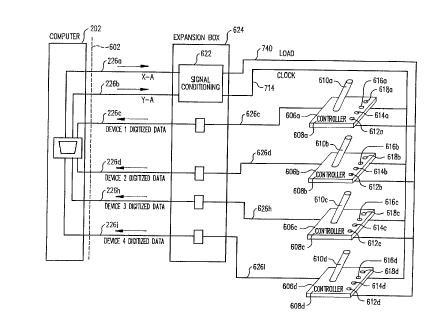
In the e..lbod.ulc.l~ of Fig. 6, four joystick devices 606a, 606b, 606c, 606d are coupled to the
c~ over the four lines 226c, 226d, 226h, 226i, l c~e~ ly, which, in previous cul.rl~;ul aliu..s,
5 wereusedforprovidingbuttoni,.ru-...A'irn Inthefml-oJ;-..~ ofFig.6,whilelines226c,226d,
226h and 226i are used for conveying inrvlllld1iun to the c--~ t~ 202, lines 226a and 226b are used
to provide i.. r.. inn from the cu. ~ ~l ul~ , in the sense that the signals on lines 226a, 226b, are
initiated, ultimately, by the c-~ - 202, but are used by external or peripheral devices coupled to the
~II~UI 1,
In the ~,.llbo-lhll~,.ll of Fig. 6, the joystick devices 606a, 606b, 606c, 606d are each provided
with controller circuitry 608a, 608b, 608c, 608d. The controller circuitry, among other filn~ticnc
digitizes(e.g.,fort~ ,ul ~storagesuchasinregistersorothermemory), ;~ru~ n ;..~ ;-.gthe
position of the joystick handle 610a, 610b, 610c, 610d, and buttons 612a-d, 614a-d, 616a-d, 618a-d, in
a manner des~l;l,ed more thoroughly below. Thus, at any given time, the register or memory in the
15 controllers 608a, 608b, 608c, 608d contain ;..rO. ~--A1;u~ indicative of the present state of the respective
control sticks and buttons.
When the c---..l.ut- - issues a ~ e.g., a write sent to 0201h, (as described more
thoroughly below) for vb1~~ g data from the joysticks, signals are sent to signal cUU~ iu~ g
circuitry such as circuitry 622, which, in the ~ ~-bo~ - .1 of Fig. 6, is located in an eYp~ncion box 624.
20 The signal con-iitir~nin~ circuitry 622 outputs a load signal to the joystick device 606a, 606b, 606c,
606d. In response, the controller 608a-608d loads the current stick and button i--fu- - ~. into one or
more output regis~ers. which may be located in the ~ C ~ box 624' (Fig. 9) or on the joystick.
T.. r~.. - - ;.~,~ from the output registers is then output serially (clocked out) e.g., on Imes 226c, 226d,
226h, 226i, lc.,~ ,ly. In one ~-..ho~l;-.-~ ~1, clock signals for clocking out data from the registers is
25 derived from write co------~--~le sent by the c-,~ u~ ~ to ~,ln~,~JUII sddress 0201h.
In order for the embodiment of Fig. 6 to operate in a fashion which is backw_d:,-comr~tihle~
a number of features or aspects of previous devices are retained. As in the previous devices, the
cullrl~ul :ion of Fig. 6 responds to a write or read signal sent to the g II~,tJUI I address (e.g., 020 Ih),
and the present cullrl~;uld~iull provides an effective l~ - e on pins 3 and 6 of the D15 plug of the
30 galll~.pOll, with a voltage on lines 226a, 226b between about zero and about 5 volts. Preferably, the
ll box c- ... -- ... ~ s ~ with the y,~ l.C~J( l l by a cable having a male D 15 plug for f ..~,~ ....l ..l
with plug 204 to provide for cu..~ .ility with existing ~ JUIl:~. Pl.,felably, new types of joysticks
608a-608d have output plugs which are different from D15 plugs to avoid inadvertently coupling a
new type of joystick directly to a conventional galII~ /UI 1. If, however, devices sre included for making
35 the new type of joystick cu- ~ .l.~l ;1 ~1 e with previous types of software, as described below, new-type
joysticks 608a-608d could be provided with a COIll~udl,iblC D 15 plug. FUI ~ -IIIUI C, because the present
hl~ ~.lliul~ provides, to the ~ ~)UI l, snalog signals on the analog lines snd button signals on the button
lines, Fig. 6 can operate in co~ lion with the installed base of ~ ,tlUIIS, i.e., using ~,CIIII~pUll:i
CA 02218706 1997-10-20
W 096/32995 PCTrUS96/05422
,,..l.~l .../;~llY identical to previous gal~ Julb 402 ~..b~ Y without the need to modify gameports.
In particular, as seen in Fig. 7, the signal cr n-liti- ning circuitry 622 can be used in c~ ...ju~ on with
interface circuitry 402 5..1.~ lly identical to that of previous devices. Thus, external devices of at
least some embodim~ntc ofthe present invention are h ~l~.a~ culllpalible with the installed base of
S ~ )01 L~
As shown in Fig. 7, the lines 226a, 226b are coupled to effective ..;,iD~.ces 704a, 704b,
which have a value selected to provide time co~ ; as de;,~;- il) ?d below. Although, in the depicted
~mho-lim.ontc resistors 704a, b are fixed resistors, if desired, variable controllable or sele~.~ble
c can be provided, e.g., for rh~nging the respective RC time c~ and/or for calibration.
10 A first RC circuit 713a is made up of capa~ilul 412a, resistor 406, and resistor 704a. A second RC
circuit 713b is made up of càlJa~;;lol 412b, resistor 406b, and resistor 704b.
With l~,L.-,.-ce to Fig. 8, at time Tl, digital data inr1ir.~ting the position and state of the control
stick and buttons for each of the joysticks 606a-606d, have been loaded into shift registers 870 by a
process which will be dc;.~,- il.cd more thoroughly below.
At time Tl the c---.. ~ 202 issues a write comm~n~l to address 0201h (in~ir~tlod in Fig. 8 by
the negali~ ~ going edge 802 of the 020 Ih write signal 804. Decoding of this write signal results in a
trigger applied to line 416, causing the opening of normally closed llal~ ul switches 418a, 418b, i.e.,
turning offthe ground-shumting llallai ,lul and allowing both the X-A ~,_I a~,ilu- 412a, and the Y-A
CayaL~;lul 412b to charge. The value of resistor 704 is selected such that the time constant of RC circuit
20 713a is relatively long (e.g., about 20 millicecu.~flc or more), providing for a relatively long period 806
required for line 226a to "time out" (i.e., reach a thl~ 1 voltage, e.g., of about 3.15v). Smce lines
226a, 226b are not ~.,hi~ - both axis lines 226a, 226b will continue charging normally until
reaching a ~ ;.. voltage.
It is ~ccllm~fi in the following de;.-,-iytiull, that valid data has already been latched in the shift
25 register 870. Initially, the first write to address 0201h will cause the first load to occur about 20
millicecnn-lc later, through a process that will be understood by those of skill in the art from the
des~.iyliùn below, of nor~nal (non-initial) register loads.
Waveform 812 shows the signal level changes which occur with a read from address 020 Ih,
which indicates charging of the X-axis line 226a. Before Irne 226a trmes out, when the charge on line
30 226a begins i..~ ;asi--g, but is below a threshold voltage defined by voltage divider 705a, e.g., 3.14v,
co, r ilu. 732 causes a transition of 738 of the load signal 740 to a high or logical one state. When
the line 226a times out, i.e., reaches the threshold voltage, cUIll~Jal i~oi 732 causes a high-to-low
transition746Ofthesignal740,ci~n~lingtheendofthereaddatatimer806. Atthistime,bitzero812
(i.e., the output from flip flop 407a placed on the first of the eight data bus lines 107 when a read at
35 201h occurs) llall ,iliOil, to a low level 752. The negative-going edge 746 of the signal at the end of the
read data tirner 806 indicates that the data, having already been latched, is ready for output to the
C~ t, .
CA 02218706 1997-10-20
W O 96~2995 PCTnUS96/05422
The resistor 704b is selected to have a relatively small ~ L~.cC to provide a relatively short
time 808 to reach the threshold voltage on line 226b established by voltage divider 705b. When the
voltage on line 226b begins increasing and/or reaches a ~JI L ~ t~ .inf d level, co-..~,~ ilu. 716 causes a
low-to-high ll all~ iOn 712 on the clock line 714. When the voltage on line 226b reaches a threshold
value, cu.. l.cuilu. 716 causes the clock line 714 to transition 722 to a low, or logical zero level, hence
co~--pl~,li -g a clock cycle. Whenever a 0201h write is p~.ru----ed at a time that the voltage on line 226b
is low or zero, a similar clock signal may be triggered. As can be seen from Fig. 8, each time the
c-....~ t~ ,s a write signal to address 0201h, while line ~6b is in the low state, a clock signal is
output on line 714. Thus, the present cullflguldLiull allows the cu~ 202 to effectively output
10 clock signals through a gS ..el.u.L to external devices such as joysticks, e.g., for purposes such as those
de.,.,.ibf d below.
While data is being clocked out of the shift register 870, in response to clock pulses 714
provided to a shift enable input of the shift register 870, the X-A axis line 226a will again be charging
832 in preparation for the ~ ,.dtiùn of the next load signal, which will typically occur about 20
15 mill;~ecf)ll~lc after the frst write to address 0201h 854, which occurs after the timing out of the
previous A-X axis signal 856.
After the timing out of the A-X axis 856, causing the load signal to also fall low 746, the first
data bit D0, 862a, is present at the serial output 626 of the shift register 870 for each of the joystick
controllers 608a, 608b, 608c, 6û8d. In response to each clock signal 714, a bit is shifted out from the
20 shift register 870 onto output line 626c.
In this way, the analog signal c~ ;---.;--g circuitry 622 detects when a write to address
û201h was ~, ,t by the c~....l---h . 202 since this is reflected by an increase in the voltage on line
226b. As ~ ;l ed above, in a response to such a write to 0201h, the signal Cf nriitioning circuitry 622
~,_.._...~s a clock pulse 714 to shift out the next data bit in the shift register 870. With each clock
25 signal 714, one bit of data is shifted from each of the controllers 608a, 608b, 608c, 6û8d onto lines
626c, 626d, 626h, and 626i ~~ .c~ vly. Although these lines could be provided directly to the
g~,~GI ~ plug 204, in' the depicted rmho.l;.. l, they are provided to the f' l~ c;~ box 624 which
couples these lines to lines 226c, 226d, 226h, 226i Cf)l ~~ ~e~,t~ d to the ~alll.,~lul l plug 204. In one
c ..bo-l;--u ..1 signals on lines 226c, 226d, 226h, 226i, are provided directly (with only the necessary
30 signal contlitioning) to the data bus lû7. Thus, the c~....l--~t~ - can retrieve the data by reading the
digital values on the data bus after each generation of a write signal to address 0201h.
In the e ..ho.l;...f ,I depicted in Fig. 8B, register 870 holds 16 bits of data, four bits provided
by analog-to-digital cu--~, t~,. 872a, IC~'IC lCIlLillg the value of variable resistor 874a, and thus, the X-
axis position of the control stick 610a. A similar conr.~,u-alion 874b, 872b provides a four-bit
35 in~lir~tinnofthey-axispositionofthecontrolstick6loa~ Pushbuttons612a,614a,616a,618a,
provide selection of 0 volts or +5 volts for storing bits into the register 870, inflir~ting the ~ IC.~:~e d or
u~d~ ,,,;,ed c~n~liti~n of the buttons 612a-618a. If desired, hard-wired circuitry 878 or, e.g., non-
volatile memory may provide a constant four-bit in~ ti~ n of the identity or type of joystick. Digital
CA 02218706 1997-10-20
W 096/32995 PCTrUS96/05422
bits 882 are input in parallel to shift register 870, I~ g the digitized location of the stick 610
and status ofthe button 612a, 614a, 616a, 618a. The load signal 740, when applied to the parallel load
enable input of the shift register 870, causes this data to be loaded, in parallel, into the shift register 870
for eventual clocking out onto line 626c in response to clock signal 714. Circuitry similar to that
5 depicted in Fig. 8B is provided in the controller 608a, 608b, 608c, 608d of each joystick 606a, 606b,
606c, 606d.
The clock r ~.lu~ ,y 714 should not exceed the highest r~ u~ at which the C~ ul, can
retrieve data from the data bus, lest the alJ~Jal aluS output 2 bits of data when the Cùlll~Jut~,l can read
only one. The L~ u.,ll~"y should be a-~ lly high that all the desired data can be tr~ncmitt~d in a
10 read cycle 806 which is a~ 1Iy short that any lag between movement of the joystick or d~ , ,;ul,
of buttons and the updating of status i..rul.--aliu.l in the CUIIIIlUt~. is small enough as to be s~h~ ;,.lly
i...~.~,.,~l,Lil,le to the user. In one embodim~-nt data is provided at a~J~Jlu~illlal~;ly one bit every 50
,..i~.. usecn. ..k
In some game cards or IDE VO cards, only two button lines are operable (e.g. as shown in
15 Fig. 3B). Thus, if an ~ -.n box depicted in Fig. 6 is coupled with such a game card, data can be
1"..,~.. .il~d only over lines 226c and 226d. This would permit use of up to 2 new-style joysticks 606a,
606b using the c~ l;n~ protocol depicted in Fig. 8. As d~ ~ - ;l-.d below, by ch~nEinE the
protocol so that the read-data timer period 806 is longer and/or the clock ~ y 714 is higher,
greater bandwidth may be available over these two lines, e.g., for a~commnA~ting ~d~litinnAl joysticks
20 or other input devices. Thus, the present invention is cull-lJdiblc with previous h~ d~ devices such
as previous g~ll~pu~b which provide only two sxis (analog) lines and/or only two buKon lines,
although p~ l ru....~lce snd/or capacity may be faster if the present i--~ iOll is used in c- .. u~ l;un with
a "full" ~a.llcpc.l (having four button lines and four analog or axis lines).
Fig. I 1 is an overview of a manner in which the cullll,ut~,l can be l-luglallllllcd to acquire dats
25 from joysticks configured ss .I~ ,.ibed above. The cc...~,ul~. 202 first issues a write comm~n~ to
sddress 0201h 1202. This causes the signal cnn~litinninE circuit to output a load pulse 238 (and a clock
pulse, which is not used at tbis time) which results in loading of data into the register 870 after about
20 ~llicluse~v~ c For example, in the embodiment of Fig. 9, in response to the load pulse, the
Illi~,lu~)luCeâavl or other control device in the ~ box will fetch dats from the joystick (which
30 may reside in registers within the joysticks or may be available for output from the joysticks in a free-
running msnner) and load the data into shift registers, such as shift registers located in th~e
i~ulJIuCf~5ùl. The GC--'~ then issues a write cnmm~nrl 1204 to address 0201h. This causes the
signal cnnrlitioninE to output a clock signal 712 which results in u.~ll ull;l~E or shifting one bit out of
each shift register onto the four lines 626c, 626d, 626h, 626i and, ultimately, onto four lines of the dats
35 bus 107. These 4 bits of dats on four lines of the dats bus can be treated in a number of fashions by the
c~..l.ul . In the ~....ho.l;.... ~.l of Fig. 12, these bits are stored 1206, e.g. in registers within the
co--.l-ul~ such ss registers 1302a, 1302b, 1302c, 1302d (Fig. 12). The write and store steps 1204,
1206 sre repeated 1208 until all 16 bits have been shifted out of the registers 870 and stored 1210 at
CA 02218706 1997-10-20
W O96/329195 PCTAUS96/05422
whieh point the ac.~ --. of data from the joystieks 608a, 608b, 608e, 608d is eomplete l212. After
completion of the l..occlul~i depicted in Fig. 12, the c~....l..~t- 202 will have stored four 16-bit words,
e.g. in fourregisters ofthe ~,v-..l---l~ -, as depicted in Fig. 12.
In the en ho~limFnt shown in Fig. 12, the first four bits stored in each of the four registers
1302a, 1302b, 1302c, 1302d located in the c~.. l.--t- -, are four-bit digitized hldi~,aliul15 of the left-right
axisloeationofthestieks610a,610b,610e,610dofthejoystieks. Thenextfourbitsintheregister
1304a, 1304b, 1304e, 1304darefour-bitdigitized.e"l. ,~ ;-ncofthefore-aftaxispo5itionofthe
control sticks 610a, 610b, 610c, 610d ofthe four joysticks.
The next bit 1306a, 1306b, 1306e, 1306d of eaeh register indieates whether eaeh of the first
10 buttons 612a, 612b, 612c, 612d is depressed. Similarly, bits 1308a-1308d indicate the status ofthe
second buttons 614a-614c, bits 310a-310d indicate the status of buttons 616a-616d and bits 1312a-
1312dindieatethestatusofbuttonsof618a-618d. Thenextfour-bitsl314a-1314dareafour-bit
i~..l;ri.~ orsi~laLul~oftheidentityortypeofjoystick606a-606d. Thedatastoredinregisters
1316a, 1316b, 1316c, 1316d of Fig. 12 can be used for any purposes for whieh the joystiek data was
15 formerly used, such as controlling games or other software.
Fig. 13 depicts an embodiment of a device driver of a type which can , '~ the
u~ c lv,~ t~,d, in u~,. vi~,~., in Fig. 11. In the embodiment of Fig. 13, the deviee driver ean be
cull~ ly eull~id_red as ;"~ g a l~ald~.alli monitor 1302 and an application plU~I mllillg
interface API 1304. The driver depicted in Fig. 13 provides an interface between ~ licaliOll~, such as
20 game software, whieh are cu--r~ d for use with the a~al_ u~ dc~,~,lil,ed above, and the p~ hc,..l
deviees c~.- .\F~ ~ d to the ~,alllC~ul L, as ~I f ~ - ;1- d above. The driver of Fig. 13 can be installed as a
tFrmin-AtF and stay resident (TSR) program, e.g., in the user's A~toFxFc bAt file. The depieted
elnbotlimFnt provides an interfaee to applieations by an interrupt handler. When an attempt is made to
install the driver it first exeeutes an inctAllAtion plu.clul~ which cheeks to deterrnine that the driver is
25 not already installed and, if not, acquires any l ~ ~vu--,~s required by the driver, such as hll~.l ul~b or
timer hooks, as d~ ,lil,ed below.
The API 13û4 provides an application l~IUE,I ll,.ling interface which is a.,cc.. ,il,le to
,.l,li- -~;....~, such as game software, via a DOS Interrupt 1306. Preferably, software sirnilar to that
depicted in Fig. 13 ean also be provided whieh is c(~ -A~il-l~ with user hlt~,.r~ces and/or Op.,~.~tlug
30 systems whieh do not use an interrupt such as Interrupt 15h. For example, Mi~luavn~ Windows and
OS/2~E9 imr~ ~ preferably do not use an INT 15h-based ealling eonvention. Instead, they
~ ef~,.dl,ly use the ~~l' ~ A~ g system's native calling conventions. Also, the driver will preferably use
the up~-al-llg system's native inter-device-driver commllnit~Ationc .l ~f ~ .~ C for the below-dc~l ;I,ed,
eallout hooks.
In the depicted Pmhorlim~nt using a DOS Interrupt, the API 1304 can use, e.g., the existing
BIOS joystick interface (INT 15h, AH = 84h), e.g., with unused ;,~ rull~lion numbers (e.g., > 80h). In
the depieted l ..,hof~ p~ all p ~ ..P~ and return values are passed in registers. In one c ..ho-l;...- -.l,
the systern uses the same registers that are used by the standard BIOS Joystick fim~tionc By using
CA 02218706 1997-10-20
W 096/32995 PCTrUS96/05422
registers, the driver can be called from DOS or from DOS ~Yfendrr.c (such as DOS4GW), without the
need for a special translation layer.
The API, as depicted in Fig. 13, is cv,lfi~,u.~,d such that, in response to a DOS Interrupt 1306,
the API 1304 will provide various services 1308 to the applications (e.g., game software), which
5 invokes or calls the API, such as by initiating a DOS Interrupt 1306. The inct~ tif~n check service
1310 det~srm inss whether the driver is installed in the system (e.g., by calling interrupt 1 Sh handler ).
If so, this ;.. r.. ~ ,- ;on is provided back to the calling program by, e.g., loading certain registers 1314
with specific constant bit patterns. Control is then returned to the calling program 1316. The
enable/disable service 1318 is an albiLIaliv~ vcclu~. An application, such as game software, must
10 enable the device driver of Fig. 13 before it starts using its services and should disable the driver before
exiting. The enable/disable service call 1318 is used by the driver to arbitrate between multiple
applications and to ac.~ui-~.h.,l~,dse ha~ uul~es.
The query cu..r~u d~ion service 1326 permits applications to send a request for i,-fvl,lla~iol-
about the nature of the attached p~ .h.,. al devices such as the number of buttons, nurnber of axes, and
15 the like. These ~Lalact~,.laLi-,s are then stored in a register for use by the calling program 1332.
The set-up service 1336 is used by the application program to set certain software switches or
mode hldi~ _-ula in the driver software, e.g., by storing values in pre-~lFtF~min~d registers 1338. For
example, the ~pli~,alivll program may instruct the driver to switch between auto-ticking and user-
ticking modes (;~F~ ed below).
The install call-out hook service 1342 is used to co.. figu,~i the driver such that other drivers in
the system can request h.r.. ~ For example, by setting software switches, such as storing values
in a register 1344, the driver can be cvl,r~ u~d to permit another driver to receive notification
~. I.c.-~ v ~ . there is a particular type of event oc. u,. i..g in the driver of Fig. 13. For example, another
driver may wish to be notified ~.I.c.,cv~,. a complete packet is latched (as described below). This
25 feature permits a IllO~allull~- to write drivers which use the devices described above to emulate other
standard PC devices. For example, using the install call-out hook feature, it would be possible to write
a mouse driver which retrieved its positional i,.ro..,,alivn from an attached new-style joystick of the
type dei..,.ibFd above, rather than from a mouse.
The read button states/axis positions 1346 service is used for an à~ ,alivll to query the
30 current state of a joystick controller stick/button position. The driver extracts h~rv~ dtiv~l from the
most recently read packet and returns the information to the application, e.g., in one or more registers.
The hàl d~. a~e monitor 1302 can be invoked in one of two ways, either by a periodic timer
interrupt handler within the driver itself ("auto-ticking" mode) or by a plurality of "ticks," each of
which is called directly by an application (the "user-ticking" mode). The user-tick request service 1352
35 is a request by the application program to perform the hai d~. ale monitor routine (as de;--,l ibed below).
In order to provide for 5nffi~ nt r~ u~,"~ of data, an application should preferably be cullrl~,u.~,d to
issue a user tick request 1352 (by issuing the ~Jlulllial~ DOS interrupt 1306) at a high frequency,
such as about 1 kilohertz.
16
CA 02218706 1997-10-20
WO 96t329~95 PCTIUS96/05422
If the driver is co.lrl~u.. d in auto ticking mode, an auto tick 1354 is periodically g~ .-_..,t~1 by
the driver itself. When the driver is cu--rl~;ul.1 to use this auto ticking mode, the driver, in one
c.--bo.li--.~,..l, hooks to a periodic interrupt (such as IRQ8, which is the real time clock (RTC) interrupt,
,.,~
or IRQ0, ~vhich is the hàl.l~ timer interrupt). The driver installs an interrupt handler for this
5 periodic interrupt.
Regardless of whether the tick is g~,,-c.~.~d by the auto-tick mode, or as a user-tick request,
the h~ monitor routine 1302 then proceeds as follows. It is first ~ d whether data is
ready for shifting out of the shift register of the external device. For example, the software can make a
i"A ;~ whether there has been a time-out 856 on line 226a (causing a load signal 738), which
10 has not yet been followed by a shifting-out of data from the shift register, such as by clock signals 714.
If data is not ready (i.e., has not been shifted out one step from the shift register onto the button lines),
the routine ;~ Iy returns or exits 1364. If data is ready, the driver then checks to
whether an entire packet of data has been received 1374. If so, the data is copied from a l~ Julal ~
buffer in the Culll~Jut~,l into a latch or arpliA~ti~n buffer 1376, such as the registers depicted in Fig. 12
15 (where the application can access the data). If the entire packet has not been received, the data on the
data bus 107 (eight bits, in the c---bo~l;---- ~.1 of Fig. 7) which was output by the driver 415, i.e. the data
provided over the button lines, is read and stored in the t-,...~u- y buffer. Thus, at any one time, the
application buffer will hold the most recently-obtained full packet of data, while the next packet is
being ~cc~m~ tAd in the t~ JUI y buffer (for eventual copying to the latch buffer, when transfer of
20 the packet is c~ ). When the data has been stored in the t~ y buffer or, as a~l~lU~JIi_~,
copied to the latch buffer, the driver will send a cnn~ to the p~ ,L_- ial devices, i.e. in the depicted
c-..hod;...~-" a write to address 201h. This will cause either or both of lines 226a, 226b (if either has
timed out) to begin charging, as depicted in Fig. 8A. The driver then returns 1316.
Several features of the l. d~ monitor routine 1302 should be noted. Preferably, the
25 l~a~d~ monitor iS designed so that the h~d~ ; monitor code 1302, which is called r~ u_.~lly
(typically at about 1 kilohertz), typically in response to a Lald~. al ~ interrupt, has a short, preferably
minimal code path, and can be executed with hll~l. u~,ta enabled. E~-,f~,.ably, the more c.. 1 ~UIAI ;~ Iy
eA~"Iahl_ work is delayed until the data is ~~ .._st~d by the applic~tion~ i.e., not during interrupt time.
In order to effect low-u~_.I._ad reads of the p~ Jh_.al device, the driver issues the clock commAn-i
30 1378attheendoftheha.. 1~.a.~imonitorroutine 1302,ratherthanatthebc~;;.. ;.. g Inthisway,data
which is loaded as a result of the C~mmAn~l 1378 sent during one iteration of the routine 1302, is
available at the be~;....;..~ of the next iteration of the routine 1302, and thus the driver does not need to
"busy-wait" for data to become a~ailal)~~ Thus the driver instructs 1378 the peli~llclal device to
perform its (relatively-slow) load operation in the "background," while application code is being
35 executed (i.e., between ticks). Because the driver does not need to idle while the external device is
loading new data, the overhead will decrease as CPU speeds increase (since more comm~n~iC can be
executed between ticks for higher CPU speeds) unlike conventional joystick routines which
CA 02218706 1997-10-20
W O 96/32995 PC~rnUS96/05422
monopolize the CPU during polling and thus consume a c~ lly constant amount of real time,
infiPpPrt-lPnt of CPU speed.
Although the embodiment of Fig. 13 is directed to a DOS il~ JII, it is possible to
provide impl.. l ~ mc for other user il~t~lr~c~s and/or uy~,lalhlg systems with, I,l,lUyliat~ changes.
S For example, under Microsoft$ Windows and OS/2~), it is generally not advisable to directly hook the
PC's hal d~. 1 timers. However, both of these operating systems provide a timer-tick service to device
drivers. The illl~l; ~ of the auto ticking mode of this driver may be different under a non-DOS
operating system. In particular, it may improve p~.ru-...al.ce to execute multiple reads (e.g., multiple
iteMtions of the Lald~.al~ monitor code) in response to a single timer tick, Mther than perform exactly
10 one read per tick. Also, because of overhead of p~,.r~,....i..g a context switch in non-DOS
c.~vi u~ c.~L" itmaybeyl~rc~al:lctonotsupportusertickingmode 1352 incertainnon-DOS
impl~.". ""~;""~
It is believed that at least some i~yl - nc of a driver generally collrl~u- ~,d acco. di..g to
Fig. 13 can be s~-~cc~r~lly operated using only about 1% of CPU time on a culllyutcl uy~..alillg at 33
15 Mhz and, about 0.4% on a 90 Mhz c-~ . It is believed that optimized versions of a driver routine
may be two to three times faster than these ~ However, in most ~ r~qc, the greater
err.ci~..cy ad~ -L. ge in the present i..~ lion arises from avoiding monopolization of the CPU for
extended periods, such as for periods of about 1.3 millicecon-lc or longer, so that, during the period the
shift register is being clocked out, the CPU can perform other tasks.
Although the driver of Fig. 13 is eccPnti~lly a time-slice (or time-sharing) polled system, it is
possible to co..rl~ an interrupt system or a pseudo-interrupt system (e.g.. a system which provides a
call-out when values are latched). In at least one ennho.l;...- ~.l. the l~,R code occupies ~ relatively
small amount of memory, such as less than one kilobyte.
In addition to the dc.,~.lil,cl method of clocking a bit of dats f~om each shiR register in
25 response to clock signals which are ~ ~d in response to write comm~nrlC data can also be sent to
the cul~yul~ . through the galllcpulL in a burst mode. In one example, burst mode can be provided
selectably, e.g. using a switch on the e~YA~ 1 box, or initiated in response to a signal sent from the
C-J---1--~t. -, e.g. two write c.,-.. ~-.-l~ sent to address 20lh within a yl~,d~,t~,ll--ined short time period.
One manner of h~yl- ~ g a burst mode is to use one of the button lines 226c to provide a clock
30 signal (prefeMbly a periodic clock signal) and placing data on the r~m~ining button lines 226d,h,i in a
manner sy,.cl..u..i~l with the clock signal, such as providing a new data bit on each of the other three
data lines each time there is a clock signal transition. In one embodiment, after burst mode is initiated,
each data burst can be initiated by, e.g. a write to address 20 Ih and can extend for a yl ~,d~ .~ . ---il.cd
period of time, ~,. . lr;. i- - . l to tMnsfer the desired number of bits over the three button lines used for
35 sending data. At each clock signal tMnsition' the Culllyutc. will store (e.g. in a buffer) v~l...t~ . data
is on the lines of data bus which cu.- ~ ,u..d to the three button lines being used to output data.
Although the depicted emho~iimPntc are generally bà~,h-.al-l~7 cu...yaLi-hle with previous
hal d~. al ~, some of the depicted operation modes are cu..r~'u. ~1 to use software such as depicted in
18
CA 02218706 1997-10-20
WO 96/32995 PCT/US96/05422
Fig. 12, which is different from that used in previous systems. According to one embodiment of the
invention, the ~ Jal~.;U~ can be c~,..fi~;ul~d to provide software c~ ;b;1ity, i.e., to provide the same
types of analog signals which older types of software are configured to make use of. In the
c.llbo.lull~ of Fig. 10, a switch 1002 is provided which can select between various modes of
5 operation. In the first position 1 004, the switch connects directly to the four joysticks and controllers,
sirnilarly to the fashion depicted in Fig. 6. In the second position 1006, the switch connects to the
output of a digital-to-analog COIl~.~,.t~,. 1008 which receives output from two joysticks 606a, 606b and
converts the digitized hlru~ d;vll into analog signals of the type similar to that output by previous
devices (as depicted in Fig. 5). In a third position 1008, the switch connects to outputs from two
10 standard joysticks 208a, 208b, to provide an effective c- .. . r;~" .. ,.~ ;.~n similar to that depicted in Fig. 2.
Although the description above ~1P . . ;1~L~ use of variable resistors 874a, 874b for converting movement
of the sticX; to an analog signal, other devices for ~vll~ IUIg IIIU ~ ~,.lle.ll to an analog signal could be
- used, such as a strain gauge, a circuit with a variable ~ l~r , or variable inductor, and the like.
Although the dc.,c~ t;vn above includes ~n~ho~lim~nt~ in which an analog signal is converted to a
15 digital sig~al by an analog-to-digital COII~ 872a, 872b, digital signals 882 can be obtained using a
digital encoder such as an optical encoder, e.g., of the type described in U.S. Patent 4,958,071, issued
Sept~qmh~r 18, 1990, c~mm~nly assigned herewith and U~-~O~UI ' herein by ~ ~ f~ . ~.-cc. If desired,
analog-to-digital co..~_.lulg circuitry can be coupled between the switch 1002 and the standard
joystick so that a standard joystick can c-~--------~;-- 't, through the ~ ,pUII in a digital fashion, e.g.
20 using the protocol depicted in Fig. 8 to provide for c-....l.d1;l.ility between new types of software and
old types of joysticks. Alt~,~uali~,ly~ instead of providing a digital to analog co..v~ tl which converts
digital data output by an u~ ll analog-to-digital C~ ., the system can be configured such that
when the switch is in the second position, c- ~--..P~ l;o-- is made with a separate line (not shown)
co."lr~,l ;..g directly to joystick variable resistors 874a, 874b to operate in the conventional fashion as
25 depicted in Fig. 4. Although Fig. 10 depicts an embodiment with a 3-way switch, other emboJullc..~
can include further choices, such as a burst-mode option, as dei.~. ibcd above. In one embodiment, the
nc ~ box 624 provides a cable which t~-minAt~ at a male D15 c~.ln. ~ I~-l, four new-style joystick
-~e~ on the box face, two standard female D15 c~ P~ on the box face, e.g., for coupling
standard joysticks, a 4-way mode switche on the box face, and a housing for the ;..I. r~- :..g and control
30 circuitry. In this emboJu--.,.-l, the mode switch allows the user to select among a new-style joystick
mode (as depicted in Fig. 6) a split mode ~ JVI tu~g a new-style joystick and two "~;alll~pàd
emulation" button devices, a "pass-through" mode 1008 and a burst-mode.
In light of the above de~ tivn, a number of advau~cs of the present invention can be seen.
The present u. ~ liun provides for c~ ~- .. - - . ;- A1 ;- -- . of infr~ ti-~n through a ~,allle~Jul I with a higher
35 ballJwiJIIl ~i.e. greater amount of ;.. ru.... ;ul- per unit time) than previous devices, preferably while
;. . ;..g hal Jw~ c-cu~ 1 ;l .ility with the existing base of cu. . .~ , having ~a~ ,ul ~. The
present ul~ ion permits use of currently existing ~;alllclJGI~ for providing, to a collll,ut~,l, data from
three or more joysticks (five or more axes) and/or a total of five or more buttons. The present
19
CA 02218706 1997-10-20
W 096/32995 PCTnUS96/05422
hl~ ~,.lliull can be cu,lfi~;ul ~ d to accommodate Cull~ iollal joysticks andlor to work with the existing
base of software. The present h.~.,..liun provides for cu~ ;orl through a ~ .u.~ in a direction
from the c~ t- - to external or p~ .al devices. The present invention provides for
C~ g ~IVI Ul ~iùnal Illu~_lllell~ or position ;..ru. ~"A1 ;nn (as opposed to simple switch
S i Irullll~ion) in a digitized form through a y, llcl)ol ~. 'rhe present i~ iu~ provides u....-...- . ~ i~ A1;. ,g
joystick or other p~ Jh~.al device i lrul--...;ion to the c-....l~ in a digitized synchronous fashion,
preferably in a S~/IICL VIIUU~ serial fashion. The present invention can provide ,- ~ rr;r: .l power to
p~ ,-al devices through the galllClJUl 1. The invention reduces or eliminates the potential for conflict
with other devices. The invention can be used without disabling illL~Ilu~ in order to service the
1 û galll~ul ~ (values are preferably latched). It is believed that, using the present invention, speed can
improve by up to a factor of about five (or more) when using a speed-cu..-~ dLi..g game port. The
present ill~,.lLiull is relatively easy for the ~IV~allllll~ to use, and does not require, for example,
counting or polling (i.e., as p~,.ru-llled in previous devices in order to dPtprminp the length of signals
522, 524, 526, 528). The present invention avoids the need to monopolize the CPU for extended
15 periods. The present invention has an Grrl~,;cn-,y which depends in part on l.lu-,c..~ul speed, as opposed
to previous devices which required a minim-lm amount of read time for each polling. The present
ill~ ~,ll~iun provides flexibility for the IJIU~allllllCI~ allowing the ~JIU~ to obtain i-- r.. ~ in a
number of different ways, e.g., by calling from the application program, by using an internal "ticker"
and the like. Because the amount of IJlo~lul~ g needed to hllpt use of the dc;.~,-il,cd device
20 c~ .,d to the joystick is smaller than that required by previous devices, the potential for
JIU~ ,- ,....--.ing errors or software ~ IuI)l~.lls is lower, thus reducing the number of technical support calls
or inquiries. The present ill~ iUn provides a device which is relatively low-cost. The presen
invention provides for relatively small amount of d~ ~ ~ lu~ - . .- - .I time and effort, e.g., preferably without
the need for providing a special application specific i.,t~ ~. t~,d circuit (ASIC). Because ill~ll u~L~ are
25 not disabled for cYtt nrl~d periods, the present invention is more easily compatible with user interface
software such as all~ Jut~,d for Miclusvn~, Windows '95, or OS/2.
A number of variations and moriifi~Ationc of the present i -~ iun can be used. It is possible
to use some aspects of the invention without using others. For example, it is possible to use the
~,alll~n~lL for Ll l;.Ç~.Iillg hlrolllldLion from the culu,~Jut~,l without l~uvidu~g data to the c~....l.llt~,~ in a
30 digitized synchronous fashion. It is possible to provide digitized S~/IICIIIUI~UU ~ data from joysticks to
the CVIll~ut~,. without providing port and/or l.cud~ i cu...l,~llil)ility of older analog joysticks.
Although the above dci,~.- il,es use of the c- .. , .. i- A1 ;on bandwidth provided through the ~;aulclJul I for
cr nnPcting e.g., to four joysticks, with four or more buttons each, the a~liti~ nAl bandwidth could be
used for other purposes such as providing more than 16 total buttons or more than four total joysticks.
Although the çmboflimPntc above describe using one of the axis lines to generate a load
signal, it is possible to dispense with this signal by providing data clocked out as a cc,llLi,luuu~ stream
freeing one of the axis lines (and the write c~mmAn~l) for other r.. ~;
CA 02218706 1997-10-20
WO 96/32995 PCT/US96/05422
Although in the depicted ennbo~lim~nt each read data cycle 806 transfers 16 bits of data ove}
each line 626c, 6Z6d, 626h, 626i, it is possible to eonfigure a system in which more or fewer bits of
data are provided in each cycle, either by making the cycle 806 longer or shorte} and/or by providing
clock signal 714 more or less rr~ u~ lly (and/or by making shift register 870 larger or smaller). More
5 data eouldl be used to, for example, provide a larger number of bits per axis to provide finer
discriminz~tion of joystick position, to provide for a greater number of button bits, and the like.
Although the depicted embodu-lclll provides data from a single joystick on each line 626c, 626d, 626h,
626i, it is possible to provide for data from 2 or more joysticks on each line, either by providing for a
greater number of data bits per write cycle, as d~ .ed above, or by using a first 16 bit word for
10 ~ ug data from the first joystick~ a next l6 bit word for l~ g data from a nextioystick~
etc. An alv~lLE,e of the configuration depicted in Fig. 6, however, is that the c- ~ ~.l~ul~ ~ is able to
identify the source of data based solely on whieh data line of the data bus the data resides on. Other
Cvl~rl~ulaLions would require di7~ "1 ;1" ' among joysticks or other input devices based on, e.g.,
timing i"Ç,lllla i-~n ~ well as data bus location.
Although Fig. 6 depicts the controllers 608a-608d residing on the joystick chassis, it is
possible for the registers and/or other controller circuitry to reside in the Ayr~nci,.n box, as depicted,
e.g., in Fig. 9. The ~mbo.li",~..,l of Fig. 9 may be used to permit coupling of joysticks 906a-906d
which do not have controllers on board as shown in Fig. 9. Since the load and clock signals are used
by the controller eireuitty, the load and clock signals can be internal to the e~ on box, thus
20 cl;. . . i. . ~fi. ~g the need to provide the load and clock signals to the joystick devices dire~tly.
The fimrtionc d- ~ ~ il.ed above as being pc.rulll,ed by cireuitry in the ~ r ~ r box, such as
the diserete CU"'I'U"- ~.I~i shown in Fig. 8B, may be partially O} fully camed out by a ~ u~essùr,
e.g., using one or more internal Illi-,lU~"U~ c~or registers as the shifl registen 8~0.
Although in the depicted embû.liull~,.lt output from up to four joysticks is provided in the serial
25 fashion over each of the output lines, it would be possible to use the output lines for ou~ut~ine data in
a parallel fashion, e.g., outr~lttin~ four A-X axis data bits in a first clock cycle, ou~ g four A-Y
axis data bits in the next clock cycle, o~ ul I ;- .~ four button bits in the next clock cycle, oullJuuillg four
X-B data bits in the next clock cycle, etc.
In one e-..bo~ ~1 circuitty can be provided to detect the type of a~J~alalu~ c.,~ d to
30 various input plugs, i.e., to detect whether a c~ t~ d device is a standard joystick, a joystick of a type
depicted in Fig. 6, or some other type (e.g., by using the i~iAntifir~ti~n bits 878), and setting the switch
1002 àCC~ iulgly.
The ~ ,pc~ll can be used with other data arqnicitifm devices than joysticks including, for
,-Y~ nrle multi-button ~;. ".,~ such as the 12-button gamepad des~,lil,cd above, head tracker
35 devices, remote control (infrared) devices, alarms and doorbells. Positional inrc ,~ iiun can be
in~lir~t~?d by means other than a stick 610, such as using a track ball, a stylus or pen, a mouse, and the
like. Although some c ...ho-i;...- -,1~ provide circuitry pu~ d on an ~ )n box and/or on
joysticks, some or all of the circuitry can be provided in the C-~ , either on an AYr~nc;on card or a
CA 02218706 1997-10-20
W 096/32995 PCTrUS96/05422
built-in fashion. Alternatively, the circuitry depicted as residing on an P~rQnQinn box can be
ln~ y all i..cu,l,u-d~d in one or more of the joysticks, e.g., with load and clock i--rol-ll~ion
being trQnQmittPd from one joystick to another in a daisy-chain fashion. Circuitry can be placed on an
PYpAnQ;r n board or built-in which uses logic rather than the circuitry of Fig. 7 to output clock and load
S signals in response to a read and/or write to address 0201h. "rhus, a new-type joystick 606a would be
c- .. "~ ;l,lc with either this new type of ~;alllc}Ju~ L interface or, by using an ~ c;.... box which could
be coupled to an old-style ~ o.t interface. In one Pnnl~o.l;...~..l it is possible to use the second axis
(Y-A axis) to restrict the number of reads in a particular time period, e.g., to restrict the rate of packet
reads to about 20 reads per second. Rc.,LI i~ tillg packet read rates can be useful in avoiding switch
10 bounce ~,.ub' - when, as is csmmon, the bouncing is not provided in the joystick. In one
embodiment, the systc-m c-~ c on average, less than about 10 mic.usecu..ds of CPU time per bit
of i..rc ....alion l~ r~ ,d to the c- -.- I-ut- - (~l~ppnfling on the speed of the c~ t~ ). Although the
embodiment depicted in Fig. 8B depicts a 16-bit shift register for each joystick device, in one
~-.. ho.l;.. .l it is possible to açcommo~lQt~ one or more joystick devices having a total of 16 buttons,
15 with two axis (proportional) controls by 32 bits of ;. . rO. . . IAl ;u~ . per read cycle. In some previous
devices, it was typical for a system in which two joysticks were coupled to a single gatne port (e.g., by
a Y c- .... P~,~u~ ) to require a . r u~illl5~tcly 1.3 millicpcnnrlc per read, or about 1.3% of elapsed time at a
read rate of 10 reads per second (since the CPU was effectively monopolized for each 1.3 millicecon-l
period and could not be used to perform other tasks, without risking loss or illacculacy of data).
20 Although the depicted Pmbo.l;..-~ generally provide for h d~al~ culll~/alilJility with the existing
base of c~ ul~ with g~..~,~u-b, the hl~,~,ntion can be h..~ c.Yt~d in a fashion is which is not
l.~d..a.~-c-....l.A1;l,1e with previous ~,allle~Jul6. For example, new types of interface circuitry can be
attached to a ~ ,c - L so that, by using the g .. c~,u. I address, other types of c~.. -- ~;~A1 ;nn can take
place. For example, the X-A and Y-A lines can be used to output, from the co,.,~ " infu""a~iol~
25 other than inru----d iu-- relating to the timing of read and write corrmQn~lc to a 0201h. The pattern of
reads and/or writes to 0201h can be used to output information and/or commands firom the co...l...t~ .
(such as using two closely spaced write to initiate a data burst. The Y-A and Y-B lines can be used to
output and/or input i..rO.... ;~... The interface can be cu--r~;ul~ d to use one or more of the button lines
for u ~ll~ull;..g data rather than for (or in addition to) inputting data. By providing for arl~iitinnAl types
30 of data output through the galllClJUl l~ other types of devices can be c- .~ P~ t~ d to the 2~alll~ l.c . L. For
example, i..ru.---ation about the status of registers or other items in the c- ....l-ut~, can be output to
p~ Jhelal devices. In this way, it may be possible for the software, e.g., to control the amount of
,k...ce which a user p~ ,.,s in the joystick, such as for cimlllAting increasing ..,si~ce to a
steering wheel when cim~ Pd driving occurs at high speeds. The device may output data to the
35 ~YpQnQion box, joystick or other p~ h~ al device for conr~;u-il,g or reprogramming the cAIJall~iull
box or pc. il~hc.al device, e.g., for A~O~ ;. .g a physical button on the joystick device with a logical
button location (dataline and/or timeslice) or changing the value of l ~ c 704a, 704b or otherwise
çhAn~inr or selecting the cn. . " " ~ ~ " ,- A1 ;onc timing or protocol. The ability to output comml-n i- Qtinn
CA 02218706 1997-10-20
W 096/32~95 PCTrUS96/05422
from the co~ ,ut~r through a galllC~JUl I to p~ Jh.,.~l devices makes it possible for the cu...~,u~,. to
query a p~ ,lal device or otherwise obtain hlru~lllalioll about p.,lil,h~,.al devices, e.g., to configure
the c~ and pc~ al device haldwal~; and/or software to operate in a desired way (so-called
"plug and play").
S Although the application has been dcsclibcd by way of pl~rtll~,d e.llbo.lil.lc~ and certain
variations and mnflifirAtinn~ other variations and mo.l;l;. A1;onc can also be used, the invention being
defined by ~e following claims: