Note: Descriptions are shown in the official language in which they were submitted.
CA 02218738 2008-01-28
1
METHOD FOR PROCESSING PWM WAVES AND DEVICES THEREFOR
Subiect of the invention.
The present invention relates to a method for processing PWM waves intended
for an inverter or a controlled rectifier, and more particularly with a view
to obtaining
the reduction of harmonics.
The present invention also relates to devices for implementing the method
according to the present invention.
Prior art relevant to the invention.
Inverters, and more particularly voltage inverters, are intended to deliver
and
AC voltage from a DC voltage, whereas controlled rectifiers are intended to
deliver a
DC voltage from an AC voltage.
In the following description, reference will more particularly be made to
inverters, but exactly the same problems arise for controlled rectifiers.
By way of example, inverters can be used for variable-speed control of
synchronous or asynchronous machines.
In this case, it is necessary to supply the load, and more particularly each
phase of a synchronous or asynchronous motor, with a three-phase voltage
system as
close as possible to a balanced sinusoidal three-phase system that can vary in
frequency and in amplitude.
Voltage inverters are well-known devices which generally use circuits of
power components such as thyristors, GTOs, etc. which switch particularly
quickly.
An inverter is controlled by a modulator and a discriminator. The role of the
modulator is to create a set wave, whereas the discriminator makes it possible
to split
this wave into a plurality of waves which are intended for individually
controlling the
various switches.
HAM_LAW\ 189984\1
. t - CA 02218738 1997-10-21
2
_ The simplest inverters have two levels and are
composed of two switches (thyristors, GTOs, etc.) which
alternately supply the load. Since this load is of the
inductive type, it is necessary for a diode referred to
as a "free-wheeling diode" to be placed in parallel
with the switch in order to allow the load current to
flow when the corresponding switch is open.
A simple square wave is customarily used as the
set wave, in order to allow switching of one or other
of the switches at each edge of the pulse. This square
wave should successively close one or other of the
switches and simultaneously open the opposite switch.
For obvious reasons of supply short-circuit, it _
is essential to check that two switches are never
closed at the same time. It is here that the
discriminator is involved, having the purpose of
introducing a delay on closure of the corresponding
switches, so that it is always certain that, when the
command to close one switch is given, the opposite
switch is already open.
This means that there is always a slight delay,
referred to as "dead time" between the instant when one
switch is opened and the instant when the opposite
switch is closed, these two operations being therefore
never simultaneous.
This is the cause of the presence of undesir-
able harmonics, and more particularly of the 5th and
7th harmonics which appear in the motor currents, this
generating the presence of a 6th harmonic on the supply
side and the drive torque side. .
In reality, it is the 6th harmonic which is the
most problematic because, for a motor supplied at 1/6
of the frequency used for signalling, there will be a
risk of interference. By way of example, the motor
supplied at 8 1/3 Hz risks causing a perturbation in
the signalling system which uses 50 Hz.
Another problem resides in the fact that the
various switches cannot switch instantaneously from a
zero value (current on, corresponding to closure) to a
f CA 02218738 1997-10-21
3
positive value of the voltage (current off and
corresponding to opening) and vice versa. This means
that, for a certain time lapse, there is simultaneously
a non-zero voltage and non-zero current, and a loss of
power is therefore observed each time switching takes
place.
In order to solve this problem, in the case
when the various components cannot sustain a power loss
of this type, it is known to propose a switching-aid
cell. An example of a cell of this type may consist
simply of a snubber which essentially comprises a
capacitor connected in parallel on each switch. The
purpose of this snubber is to absorb the power losses
by limiting the voltage, and more particularly by
limiting its growth, on switching. Another example of a
cell which is often used in combination with the
snubber is the so-called "di/dt" cell, which
essentially comprises an inductor in series w'ith the
switches. Because of the presence of these various
switching-aid cells, a slower increase in the voltage
is observed, which makes it possible to limit the power
losses on switching.
The problem of the presence of harmonics is
essentially the same for an inverter with or without a
switching-aid cell. In particular, the presence of 5th
and 7th harmonics on the motor side is also observed in
the case of using an inverter with a snubber, as is the
presence of the 6th harmonic on the supply side and the
drive torque side.
It should be noted that, in the case of
controlled rectifiers, exactly the same problems arise,
except for the fact that the load should in this case
be considered as the source, and the supply as being
the load.
Objects of the invention.
The object of the present invention is to
provide a method which makes it possible to reduce, or
eliminate, the effect of the dead times in an inverter
or a controlled rectifier, and therefore makes it
CA 02218738 1997-10-21
4
-possible to reduce the effect of the undesirable
harmonics.
The object of the present invention is, in
particular, to provide a method which can be applied to
inverters or control rectifiers, with or without a
switching-aid cell, irrespective of whether they have
two levels or multiple levels.
In particular, the object of the present
invention is, in the case of a three-phase inverter
supplying a synchronous or asynchronous motor, to
provide a method which makes it possible to reduce the
undesirable harmonics such as the 5th and 7th harmonics
appearing in the motor currents, and thereby the 6th
harmonic appearing on the supply side and the drive
torque side.
Principal characteristic elements of the invention.
The present invention relates to a method for
processing PWM waves intended for a voltage inverter or
a voltage-controlled rectifier, comprising at least one
pair of switches, this inverter or rectifier being
controlled by a modulator and a discriminator,
characterized in that two set signals, corrected as a
function of the direction of the current in the load or
in the source, are applied to the discriminator, the
set signal corrected for the output current having a
high state supplemented by a delay on transition from
the high state to the low state, and the set signal
corrected for the input current having a low state
supplemented by a delay on transition from the low
state to the high state, the high state being defined
by the fact that the switch connected to the most
positive load is closed whereas the switch connected to
the most negative load is open, the low state being
defined by the reverse.
In the case when the inverter or rectifier does
not have a switching-aid cell, the corrected set
signals introduce delays which correspond to the dead
time created itself by the discriminator.
CA 02218738 1997-10-21
In the case involving an inverter or rectifier
with a switching-aid cell, the delay introduced in the
corrected set signals depends not only on the direction
of the current but also on its value.
5 It should be noted that the present method can
be applied equally well to inverters or rectifiers with
two levels and to multi-level inverters or rectifiers.
The present invention also relates to a device
for implementing the method.
Brief description of the figures
The present invention will be described in more
detail with reference to the following figures:
Figure 1 represents a schematized view of a branch of
a conventional two-level inverter.
Figure 2 represents the set wave (Fig. 2a) created by
the modulator for an inverter as described in
Figure 1, as well as the waves which are
obtained at the output of the discriminator
and are intended for directly controlling the
switches (Figs. 2b and 2c) and the
corresponding voltages applied in this case
to the motor (Figs. 2d and 2e).
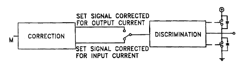
Figure 3 represents a block diagram of a device for
implementing the method according to the
invention.
Figure 4 represents the corrected waves (Figs. 4b and
4c) for a given set wave (Fig. 4a) to be
applied to a two-level inverter as described
in Figure 1 in order to implement the method
according to the present invention as well as
the output voltages applied in this case to
the motor (Figs. 4d and 4e).
Figure 5 represents a schematized view of a branch of
a conventional two-level inverter with a
snubber.
Figure 6 represents the setwave (Fig. 6a) created by
the modulator and intended to control an
inverter as described in Figure 5, as well as
the output voltages applied in this case to
CA 02218738 2006-06-06
6
the motor for a low or high input current (Figs. 6b and 6c) and
for a low or high output current (Figs. 6d and 6e), Figs. 6f and 6g
representing details of Figs. 6b and 6c.
Fig. 7 represents the general shape of the motor current, on the one
hand when not applying the method according to the present
invention (Fig. 7a), and on the other hand, applying this method
(Fig. 7b).
Description of Several Preferred Embodiments of the Invention
In this section, the description is limited to a two-level inverter.
The person skilled in the art will find it easy to generalize this description
to a
multi-level inverter as well as to a two-level or multi-level rectifier.
Fig. 1 schematically represents a branch of a conventional two-
level inverter which is used in the fashion, this inverter comprises two
switches S1 and S2 which alternately supply a load that may, for example, be
a phase of an asynchronous motor. In this case, the load is of the inductive
type and it is necessary for each of the two switches S1 and S2 to be
connected in parallel with a diode, which is referred to as a "free-wheeling
diode" DR1 or DR2, which allows the load current to flow when the
corresponding switch is open. Indeed, the presence of this diode allows the
inductive load current to decrease and thus makes it possible to avoid any
destructive overvoltage when the corresponding switch is opened.
CA 02218738 1997-10-21
7
The inverter is controlled by a modulator and a
discriminator.
Figure 2a represents a set wave M which is in
the form of successive pulses. When the high level 1 is
reached, this means that the switch Sl is to be closed
and the switch S2 is to be open. Conversely, when the
low level 2 is reached, the switch S2 is to be closed
whereas the switch S1 is to be opened. Consequently, at
each leading or trailing edge, it is necessary to
switch instantaneously the switch S1 in order to close
it and the switch S2 in order to open it, or vice
versa.
Of course, a check should be made that the two
switches (S1 and S2) are never simultaneously closed,
which would short-circuit the supply. In order to avoid
this situation, the instant when one switch is closed
is delayed for a certain length of time after the set
signal has been given. In reality, this t~ask is
performed by the discriminator.
Figures 2b and 2c represented the waves which
are modified by the discriminator and which will
control the two switches SI and S2. As can be seen, the
closure of a switch turning the branch on does not take
place instantaneously, but happens with a delay
referred to as the "dead time", whereas the opening
leading to a break may be considered as instantaneous.
As can be seen in figures 2b and 2c, the two
switches are never simultaneously closed. Conversely,
in certain cases, the two switches Sl and S2 may be
considered as opened simultaneously.
The result of this is that at least one of the
two free-wheeling diodes DR1 or DR2 will be on during
the dead times, this depending on the direction of the
current. Specifically, when the current is an output
current, it is the lower diode DR2 which is on during
the dead time, thus reducing the high-level time of the
output voltage (see curve 2d) . In the opposite case,
with an input current, it is the upper diode DR1 which
CA 02218738 1997-10-21
8
_is on during the dead time, in this case increasing the
high-level time of the output voltage (see curve 2e).
It should, however, be noted that this
phenomenon is variable, since it depends on the
direction of the current.
With the assumption that the switches respond
instantaneously to the set signal M, that is to say
with the assumption that there is no dead time between
the set signal M and the response of the switches, it
is found that 5th and 7th harmonic levels correspond to
theory and do not significantly perturb the motor
currents.
Nevertheless, because of this presence of a
dead time on switching to closure, an increase in the
5th and 7th harmonics is observed in the motor
currents, as well as in the 6th harmonic on the supply
side and the drive torque side. This harmonic is
particularly problematic for the reasons set out=above.
The object of the present invention is to
provide a solution to this problem by suggesting the
use of two corrected control set signals, one for the
case when the current is an output current and the
other for the case when the current is an input
current.
Figure 3 represents a block diagram of a device
for controlling a conventional two-level inverter by
using the method according to the present invention. In
this case, the discriminator is either controlled by a
set signal corrected for an output current, or by a set
signal corrected for an input current. It is the
direction of the current in the load which will
determine whether one or other of the two corrected set
signals is used.
Figure 4 represents the ideal set wave M(Fig.
4a) and each of the two corrected set signals, on the
one hand for the output current (Fig. 4b) and on the
other hand for the input current (Fig. 4c). As can be
seen in the case of a set signal corrected for an
output current, the high level 1 is supplemented by a
CA 02218738 1997-10-21
9
.time Tm which, in the present case, corresponds to the
dead time on the trailing edge, that is to say on a
transition from the high state 1 to the low state 2.
This transition corresponds in reality to the opening
of the switch 1 and to the closure of the switch 2. The
set signal corrected for the input current has a high
level 1 decreased by a time T. which also corresponds to
the dead time at each leading edge, that is to say on
transition from the low state 2 to the high state 1.
Furthermore, Figures 4d and 4e represent the
output voltages in the case when corrected set signals
are used, either for an input current or an output
current. It is observed that the correction allows the
output voltage of the inverter to be made identical in
both cases, and identical to what it would be without a
dead time, to within a delay Tm.
Figure 5 represents a schematized view of a
branch of a conventional two-level inverter 'with a
snubber.
This snubber is in reality a switching-aid
cell, which makes it possible to absorb the power
losses which occur each time the switches Sl and S2 are
switched, by limiting the voltage, and more
particularly by limiting its increase.
As represented in Figure 5, this cell comprises
a capacity Cl (or C2) connected in parallel on each
switch, this capacitor being itself in series with a
resistor R1 (or R2) as well as a second diode Dl (or
D2) which is in the opposite direction to the free-
wheeling diode DR1 (or DR2).
When a switch S1 (or S2) is opened, this makes
it possible to divert the current to the corresponding
capacitor Cl (or C2), which was initially uncharged.
When the switch S1 (or S2) is closed, the
corresponding capacitor Cl (or C2) discharges through
it. In this case, the discharge current will be limited
by the presence of the resistor Ri (or R2) in series
with the capacitor CI (or C2), thus forming an RC
circuit.
CA 02218738 1997-10-21
In general, each time switching takes place, it
is observed that one of the two capacitors will charge
whereas the other starts to discharge through its
associated resistor.
5 A slower increase in the voltage is then
observed, thus limiting the power loss from switching.
Figure 6 represents the set wave M (Fig. 6a) as
well as the corresponding voltages applied to the motor
in the case of a low input current (Fig. 6b), in the
10 case of a high input current (Fig. 6c), in the case of
a low output current (Fig. 6d) and in the case of a
high output current (Fig. 6e).
Let us analyse in more depth the case of an .
input current on a low/high transition of the set'
signal M, that is to say in the case when the switch S1
is to close whereas the switch S2 is to open (Figs. 6f
and 6g).
In this figurative case, it is found that the
initially zero output voltage cannot increase instant-
aneously. This is because. it is first necessary to
charge the capacitor C2 of the lower snubber using the
current.
If the current is high, the voltage rises
quickly and the output voltage rapidly reaches the
supply voltage. In this case, the upper free-wheeling
diode DR1 conducts and allows the current to flow to
the supply (Fig. 6g).
In the case when the current is low, the output
voltage applied to the motor remains less than the
supply voltage at the end of the.dead time. At this
moment, the switching of the upper switch Sl takes
place and the capacitor C2 of the lower snubber is
charged suddenly (Fig. 6fj.
This means that a deformation is observed in
the voltages supplied to the motor, this depending both
on the direction of the current and also on its value.
For this reason, a corrected set signal should
be proposed which depends not only on the direction of
CA 02218738 1997-10-21
11
the current but also on its strength, in the case of
controlling an inverter with a switching-aid cell.
In particular, the corrected set signal should,
depending on whether an output or an input current is
involved, have a level 1 supplemented or reduced by a
time corresponding to a time referred to as the
"effective time", which takes into account the value of
the current.
In practice, for a certain current IT, the
charging time of the snubber is equivalent to the dead
time, namely
C X Uo
Ir=
Td..d
For I > IT, the effect of the dead time is
equivalent to a delay Teff:
I
T,ff =Tawd 1-
For I < IT, the effect of the dead time is
equivalent to a delay Tetf=
{I{
T ff _ Td. d 2I
r
In this way, compensation is thus made for the
actual effect of a dead time on switching to closure,
and the level of the 6th harmonic on the supply side is
reduced.
It should be noted that, in certain cases, and
more particularly in the case when a current is low,
and irrespective of the direction of this current, it
may be envisaged not to use corrected set signals. This
is because, in the case of low currents, the influence
of these corrections is relatively limited.
Furthermore, Figures 7 represent the general
appearance of the motor currents, either in the case
when the method according to the present invention is
CA 02218738 2006-06-06
12
not applied (Fig. 7a), or in the case when this method is applied (Fig. 7b),
for
an inverter without a snubber.
Elimination is observed of the distortion due to the presence of a
dead time which exists in the case when correct set signals are not used, by
applying the method according to the present invention.
Exactly the same performance can be obtained for an inverter
with a snubber.