Note: Descriptions are shown in the official language in which they were submitted.
CA 02218829 1997-10-22
ASYN~H~Or70US TRANSFER MODE S~1-~.n1NG SYSTEM
R~ OUND OF THE 1NV~L.~10N
The present invention relates to an ATM (asynchronous
transfer mode) switching system.
In conventional ATM switching systems with a small
switching capacity of about 2.4 Gbps, the dominant systems
are of a simple input/output buffer type, as shown in Fig.
22, in which a high rate time division multiplex bus :
directly accommodates a low rate line interface usable by
a user terminal.
The cell switching operation of an ATM (Asynchronous
Transfer Mode) switching system with the conventional
configuration will be described below. A class/line
separator 112 identifies ATM cells flowed through the
input line liO~by their destination output lines and
service class types and then stores them to proper output
line corresponding queues 111.
The rotation priority control section 108 controls such
that a cell sending right is handed over in rotation
between output line corresponding queues 111 belonging to
the same service class. The interclass priority control
section 109 controls competition for cell sending requests
between different service classes in accordance with a
prèdetermined priority control theory
CA 02218829 1997-10-22
There are CBR (Constant Bit Rate), VBR (Variable Bit
rate), ABR (Available Bit Rate), and UBR (Unspecified Bit
Rate) as the service class.
The ATM cells, which are selected through a combination
process of the rotation priority control section 108 and
the interclass priority control section 109 and taken from
the output line corresponding queue 111, are stored into
the core switch queue 103 corresponding to the destina,,tion
output line via the time division multiplex bus 104.
The core switch key 103 sequentially sends out ATM cells
from the leading cell to the output llne 101. The buffer
occupancy computing section 105 in the core switch section
102 observes the queue length (buffer occupancy) of the
core switch queue 103. The back pressure originating
section 106 refers to the queue length information of the
core switch key~ 103 holding the buffer occupancy computing
section 105, and then originates the back pressure signal
- 113 specifying an output line in a congestion state to all
input buffer module sections 110 when it detects that a
core switch queue 103 in a congestion state exists because
of the queue length exceeding a threshold value.
The back pressure receiving section 107 in the input
buffer module section 110 specifies the output line
originating a back pressure signal based on back pressure
signal information received, and then reports the rotation
CA 02218829 1997-10-22
priority control section 108 to inhibit sending cells from
the output line corresponding queue 111 corresponding to
the output line.
AS described above, as traffic control between an input
buffer and an output buffer in an ATM switching system
with the conventional configuration, there has been only
the simple back pressure control which originates a back
pressure signal instructing to halt the outputting of~a
cell to a specific output line to all input buffer modules,
in order to prevent the cell loss in the output buffer in
the case of congestion of the specific output line.
In order to increase the switching capacity, the
conventional method described above is made of the scheme
of accommodating many low rate interfaces using higher
rate time division multiplex bus. However, because the
increasing numb~er of input/output signals on the time
division multiplex bus causes, for example, a shortage of
- the number of pins, it is difficult to realize the scheme
in view of packaging on LSTs.
The conventional ATM switching system frequently
originates back pressure signals to prevent a cell loss
occurring in the output buffer because congestion occurs
frequently because of simultaneous arrival of ATM cells to
the same line from plural input lines.
Basically, the back pressure control has the effect of
CA 02218829 1997-10-22
equalizing the throughput issued from each input line to
the same output line. When the number of VCs (Virtual
Channels) connected to the same output line is varied
between input lines, the throughput evenness cannot be
secured between VCs using the same output lines. Hence,
in the conventional ATM switching system, the problem is
that frequent occurrence of the back pressure signals
causes the throughput evenness.
SUMMARY OF THE lNv~N-llON
The objective of the present invention is to solve the
above-mentioned problems. The objective of the invention
is to provide an ATM switching system that can easily
increase its switching capacity and an effective
throughput by suppressing occurrence of congestion inside
an ATM exchange, so that the throughput evenness can be
guaranteed betwteen virtual channels using the same output
1 lnes .
- The objective of the present invention i~ achieved by
the ATM switching system comprising a switch section for
storing an ATM cell into a buffer to implement an ATM cell
exchange between an input port and an output port at a
predetermined transmission rate; an input buffer module
section having a buffer that multiplexes plural input
lines with a transmission rate slower than the
predetermined transmission rate to the input port of the
CA 02218829 1997-10-22
switch section and then stores the ATM cell; and an output
buffer module section having a buffer that separates an
output from the output port of the switch section into
plural output lines with a transmission rate slower than
the predetermined transmission rate and then stores the
ATM cell; the input buffer module section which enables
queuing from the ATM cell to the buffer for each of the
output lines and for each service class accommodated by
the input buffer module section itself; the output buffer
module section which enables queuing to the buffer for
each destination output line and for each service class;
the output buffer module section including means for
originating a cell inhibit signal to the switch section
when the total occupancy of the buffer exceeds a
predetermined threshold value; queues respectively placed
for~the output~lines; and means for originating a cell
inhibit signal to all the input buffer module sections
when the length of each of the queues exceeds a
predetermined threshold value; the switch section
including queues respectively placed for the output ports;
means for originating a cell inhibit signal to all the
input buffer module section when each of the queues
exceeds a predetermined threshold value; and halt control
means for halting a cell transmission to the output buffer
module section to which the cell inhibit signal has
CA 02218829 1997-10-22
originated; the input buffer module section including the
output port to which the cell inhibit signal is
originated; and halt control means for halting a cell
transmission to the output line.
According to the ATM switching system, the input buffer
module section further comprises an output line
corresponding queues respectively placed for the output
lines, and a virtual queue being a set of queues for the
same output port among the queues. The output buffer
module section further comprises rate computing means for
periodically computing an acceptable rate of a queue for
each of the output lines in the output buffer module
section.
According to the ATM switching system, the rate computing
means periodically computes an acceptable rate for each
service class ~ased on a status time change of the virtual
queue by service class or the output line corresponding queue
- of the output buffer module section. The i~put buffer module
section further includes an internal rate control means that
controls a cell transmission for each output line based on
the acceptable rate.
According to the ATM switching system, the output line
corresponding queue has a double structure including a first
queue and a second queue in the input buffer module section.
Thè internal rate control means is placed between the first
CA 02218829 1997-10-22
-- 7
queue and the second queue to control cell transfer from the
first queue based on the virtual queue or an acceptable rate
computed by means of the rate computing means in the output
buffer module section.
According to the ATM switching system, among a product of
an acceptance rate computed using the virtual queue for an
output port corresponding to the output line corresponding
queue and the number of active logical channels in which a
cell is stored into an output line corresponding queué in the
output buffer module section corresponding to the output line
corresponding queue at a current time and a product of an
acceptable rate computed using an output line corresponding
queue in the output buffer module section corresponding to
said output line corresponding queue and the number of active
logical channels in the output line corresponding queue, a
smaller product is used as a transfer rate to be set to the
internal rate control means in the output line corresponding
- queue within the input buffer module section.
Moreover, according to the ATM switching system, the buffer
occupancy of an output line corresponding queue of the input
buffer module section is observed for each logical channel,
and discards a packet when a buffer occupancy of the logical
channel of the packet in the output line corresponding queue
exceeds a predetermined threshold value upon arrival of the
leading cell of the packet to the output line corresponding
CA 02218829 1997-10-22
queue.
According to the ATM switching system, a value obtained
by dividing a fixed threshold value by the number of
active logical channels of the output line corresponding
queue is used as a value compared with a buffer occupancy
of the logical channel of the packet in the output line
corresponding queue of the input buffer module section.
In order to solve the above-mentioned problem, according
to the present invention, the ATM switching system
comprises a core switch section in an output buffer-type
configuration for realizing ATM cell exchanges between
high rate input and output ports; an input buffer module
section for multiplexing plural low-rate input lines to a
high-rate input port in the core switch section; and an
output buffèr module for separating an output from a
high-rate output port in the core switch section into
plural low rate output lines; the input buffer module
- section enabling queuing for each output llne and for
each service class; the output buffer module section
enabling queuing for each output line and for each
service class accommodated by the output buffer module
section itself.
In order to prevent a cell loss in the core switch
section and the output buffer module section within the
ATM switching system with above-mentioned configuration, a
CA 02218829 1997-10-22
back pressure signal is originated to all extended input
buffer module sections when the core switch queue length
prepared for each output port in the core switch section
exceeds a threshold value. Moreover, a back pressure
signal is originated to the core switch section when the
total buffer occupancy in the output buffer module section
exceeds a threshold value. Moreover, a back pressure
signal is originated to all the input buffer modules when
each output line corresponding queue length in the output
buffer module section exceeds a threshold value. The input
buffer module section prepares back pressure control under
which a cell to be output to the output port or output
line originating a back pressure signal is suspended. The
core switch section prepares back pressure control under
which a cell to be output to the output buffer module
section origina~ting a back pressure signal is suspended.
In order to increase the throughput for each output line
by suppressing frequent occurrence of internal congestion
in the ATM switching system with the above-mentioned
configuration and to improve the throughput evènness
between virtual channels using the same output line, and
to use effectively the buffer in the output buffer module
section, the rate computing function is prepared that
respectively and periodically computes a virtual queue
(global queue) being a set of output line corresponding
CA 02218829 1997-10-22
-- 10
queues for the same output port among all output line
corresponding queues in the input buffer module sections,
as well as an acceptable rate in the output line
corresponding queue within the output buffer module
section. The output line corresponding queue within the
input buffer module section has a double structure formed
of a virtual source queue and a virtual switch internal
queue. The rate control section placed between the virtual
source queue and the virtual switch internal queue
controls cell transfer from the virtual source queue to
the virtual switch internal queue based on an acceptable
rate computed using a global queue or an output line
corresponding queue in the output buffer module section.
In order to perform uniform rate control between logical
channels (VC) by means of the rate control section in the
input buffer m~dule section, the buffer occupancy of the
output line corresponding queue within the input buffer
- module section is observed for each logical channel (VC).
Thus, when the buffer occupancy of the logical channel
(VC) in a packet exceeds a threshold value upon arrival of
the leading cell of the packet to the output line
corresponding queue in the input buffer module section,
the packet is discarded.
BRIEF DESCRIPTION OF THE DRAWINGS
This and other objects, features and advantages of the
CA 02218829 1997-10-22
-- 11 --
present invention will become more apparent upon a reading
of the following detailed description and drawings, in
which: -
Fig. 1 is a block diagram showing an ATM switching
system according to an embodiment of the present
nvent ion;
Fig. 2 is a diagram showing the configuration of a
buffer occupancy information table held by the buffer
occupancy computing section in the input buffer module
section according to the embodiment in Fig. l;
Fig. 3 is a diagram showing the configuration of a
buffer occupancy information table held by the buffer
occupancy computing section in the core switch section
according to the embodiment in Fig. l;
Fig. 4 is a diagram showing the configuration of a
buffer occupan~y information table held by the input
buffer occupancy computing section in the output buffer
module section according to the embodiment-in Fig. l;
Fig. S is a morphological diagram showing the back
pressure control according to the embodiment in Fig. l;
Fig. 6 is a diagram showing an acceptable rate
computation environment in the embodiment of Fig. l;
Fig. 7 is a flow chart showing a packet-selection
discarding process in the embodiment of Fig. l;
Fig. 8 is a state diagram explaining a process procedure
CA 022l8829 l997-l0-22
- 12
of switching an ATM cell between an input line and an
output line in the embodiment of Fig. 1;
Fig. 9 is a state diagram explaining a process procedure
of switching an ATM cell between an input line and an
output line in the embodiment of Fig. 1;
Fig. 10 is a state diagram explaining a process
procedure of switching an ATM cell between an input line
and an output line in the embodiment of Fig. 1;
Fig. 11 is a state diagram explaining a process
procedure of switching an ATM cell between an input line
and an output line in the embodiment of Fig. 1;
Fig. 12 iS a state diagram explaining a process
procedure of switching an ATM cell between an input line
and an output line in the embodiment of Fig. 1;
Fig. 13 is a state diagram explaining a process
procedure of sw~itching an ATM cell between an input line
and an output line in the embodiment of Fig. 1;
- Fig. 14 is a state diagram explaining a process
procedure of processlng plural ATM cells arrived
simultaneously when the core switch queue length is less
than BP_CS signal generation threshold value, in the
embodiment of Fig. 1;
Fig. 15 is a state diagram explaining a process
procedure of processing plural ATM cells arrived
simultaneously when the core switch queue length is less
CA 022l8829 l997-l0-22
- 13
than BP_CS signal generation threshold value, in the
embodiment of Fig. l;
Fig. 16 is a state diagram explaining a process
procedure of processing an ATM cell arrived when the
buffer occupancy of an output buffer module section is
less than a threshold value for BP_OXB signal generation,
in the embodiment of Fig. l;
Fig. 17 is a state diagram explaining a process
procedure of processing an ATM cell arrived when the
buffer occupancy of an output buffer module section is
less than a threshold value for BP_ OXB signal generation,
in the embodiment of Fig. l;
Fig. 18 is a state diagram explaining a process
procedure of processing an ATM cell arrived when the
output line corresponding queue in an output buffer module
section is less~ than a threshold value for BP_ OXBL signal
generation, in the embodiment of Fig. l;
- Fig. 19 is a state diagram explaining a process
procedure of processlng an ATM cell arrived when the
output line corresponding queue in an output buffer module
section is less than a threshold value for BP_OXBL signal
generation, in the embodiment of Fig. l;
Fig. 20 is a state diagram explaining a process
procedure of setting an acceptable rate to the rate
control section within an input buffer module section, in
CA 022l8829 l997-l0-22
- 14
the embodiment of Fig. l;
Fig. 21 is a state diagram explaining a process
procedure of judging whether or not a packet can be
received when the leading cell of a packet arrives at an
input buffer module section, in the embodiment of Fig. l;
and
Fig. 22 is an ATM switching system with a conventional
configuration.
DESCRIPTION OF THE EMBODIMENTS
Next, an embodiment of the present invention will be
described below in detail with reference to the attached
drawlngs.
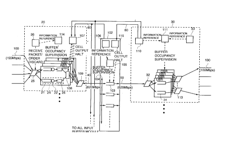
Fig. 1 is a block diagram showing the configuration of
an ATM switching system according to an embodiment of the
present invention. The ATM switching system consists of a
core switch sec,tion (CS section) 102, an input buffer
module section (IXB section) 20, and an output buffer
- module section (OXB section) 30.
The core switch section 102 is a simple switch of the
output buffer type which provides an ATM cell switching
function between a high-rate input port and a high-rate
output port. The input buffer module section 20
multiplexes plural low rate input lines 100 and mediates
in connection to the high-rate input port of the input
buffer module section 102. The core switch section 102
CA 022l8829 l997-l0-22
- 15
includes an output circuit corresponding queue 24 to
enable a queuing operation for each output line. The
multi-service class environment can be easily provided by
preparing the output line corresponding queue 24 by each
service class. In the present embodiment, the output line
corresponding queues 24 are prepared corresponding to four
service classes (CBR, VBR, ABR, UBR). The output line
corresponding queue 24 can be prepared by a desired nu~mber
f
o servlce c asses.
The input buffer module section 20 includes a buffer
occupancy computing section 114 for observing the buffer
occupancy for each of VCs in each output line
corresponding queue 24 and a packet acceptance control
section 26 for controlling a packet selection discard
based on the observed buffer occupancy.
The output liine corresponding queue 24 in the input
buffer module section 20 has a double configuration
- including a virtual source queue 21 and a virtual switch
internal queue 23 sandwiching a rate control section 22.
The rate control section 22 controls the cell transfer
rate from the virtual source queue 21 to the virtual
switch internal queue 23, to a designated rate.
The output buffer module section 30 aims at separating
the traffic from a high-rate output port 50 of the core
switch section 102 into plural low-rate output lines 101.
CA 02218829 1997-10-22
The output line corresponding queue 31 enables queuing for
each output line accommodated by itself. Like the input
buffer module section 20, the output buffer module section
30 can easily provide the multi-service class environment
by preparing the output line corresponding queue 31 for
each service class.
The output buffer module section 30 includes a virtual
queue (global queue) formed of a set of output line
corresponding queues 24 for the same output port among the
output line corresponding queues 24 in all the input
buffer module sections 20, and an acceptable rate
computing section 33 for computing an acceptable rate in
the output line corresponding queue 31 within the output
buffer module section 30.
The output buffer module section 30 uses a completely-
shared buffer s~cheme in which each logical queue can
freely use the full buffer capacity. The input buffer
- module section 20 has the structure that s$ts an upper
limit for each logical queue so that a specific logical
queue cannot monopolize the full buffer capacity.
The cell switching operation of an ATM switching system
according to the present invention will be explained below.
In the input buffer module section 20 accommodating plural
input lines 100, the class/line separator 25 identifies
the destination output line and the service class type of
CA 02218829 1997-10-22
an ATM cell flowing from the input line 100, and stores it
into a proper output line corresponding queue 24. The
output line corresponding queue 24 is formed of a virtual
source queue 21, a rate control section 22, and a virtual
switch internal queue 23.
The ATM cell is first stored into the virtual source
queue 21, and is moved from the virtual source queue 21 to
the virtual switch internal queue 23 at a transfer rate
provided by the rate control section 22. The rotation:
priority control section 108 controls such that the cell
transfer right is taken in turn between the output line
corresponding virtual switch internal queues 23 belonging
to the same service class. The interclass priority control
section 109 controls the competition between cell transfer
requests from different service classes according to a
predetermined p~riority control logic.
The ATM cell taken from the virtual switch internal
queue 23 selected by means of a combination process of the
rotation priority control section 108 and the interclass
priority section 109 is stored into the core switch queue
103 corresponding to the destination output port via the
time division multiplex bus 104. The core switch queue
103 transmits the ATM cells to the successive output
buffer module 30 through the output port 50, in order of
the leading cell.
CA 022l8829 l997-l0-22
- 18
In the buffer module 30, the class/line separator 32
identifies the destination output line and the service
class type of an ATM cell, and stores a proper output line
corresponding queue 1. The interclass priority control
section 113 prepared for output line selects a service
class to be next transmitted among output line
corresponding queues 31 in each service class storing
cells for the same output line, according to a
predetermined priority control logic, and then transmlts
the leading cell to the output line 101.
Fig. 2 illustrates an example of information contents
held by the buffer occupancy computing section 114 in the
input buffer module section 20. Fig. 3 illustrates an
example of information contents held by the buffer
occupancy computing section 105 in the core switch section
102~ Fig. 4 il~ustrates an example of information contents
held by the buffer occupancy computing section 111 in the
- output buffer module 30. The buffer occupa~cy computing
section 114 in the input buffer module section 2, as shown
in Fig. 2, holds the entire queue length including the
virtual source queue 21 and the virtual switch internal
queue 23 in the output line corresponding queue 24 of each
service class, virtual switch internal queue length, the
buffer occupancy of the entire queue length for each VC,
and the like.
CA 02218829 1997-10-22
-- 19
The buffer occupancy computing section 105 in the core
switch section 102, as shown in Fig. 3, has the queue
length of each core switch queue 103. The buffer occupancy
computing section 111 in the output buffer module section
30, as shown in Fig. 4, stores the buffer occupancy 202 in
the output line corresponding queue 31 of each service
class as well as each output line corresponding queue
length 203 forming the global queue for the output buffer
module section 30.
Fig. 5 is a schematic diagram showing the back pressure
control in an ATM switching system according to the
present invention. For the brief explanation, the
configuration is shown as to the case where only one
service class exists. In the core switch section 102, when
the queue length Qcs of the core switch queue 103 prepared
for each output~port 50 exceeds the threshold value
Qth_bpcs, a back pressure signal (BP_CS) 60 is originated
to all the input buffer module section 20.
The input buffer module section 20 stops transmitting
cells to the output port which has originated the BP_CS
signal. In the environment where plural service classes
exist in a mixed state, control can be performed according
to various service class quality requests by preparing the
threshold value Qth_bpcs for each service class or
applying one BP_CS signal to plural service classes.
CA 022l8829 l997-l0-22
- 20
On the other hand, when the total buffer use amount Qoxb
exceeds the threshold value Qth_bpoxb, the output buffer
module section 30 originates a back pressure signal
(BP_OXB) to the core switch queue 102 at the previous
S tage.
When receiving the BP_OXB signal 80, the core switch
queue 103 ceases to output a cell to the successive output
buffer module section 30 which has originated it. In each
output line corresponding queue within the output buffer
module section 30, when the queue length Qoxbl exceeds the
threshold value Qth_bpoxbl, the output buffer module
section 30 originates the back pressure signal (BP_OXBL)
70 to all input buffer module sections.
The input buffer module section 20 ceases to transmit
cells to the output line to which the BP_OXBL signal 70
has~been origi~ated. Since the Qth_bpoxbl can be
independently prepared for each output line corresponding
- queue prepared by service class, control can be performed
according to a variety of service class quality requests.
AS described above, in the comparison of the switch
configuration according to the above embodiment of the
present invention which directly accommodates higher rate
port interfaces with the conventional scheme which
directly accommodates lower rate port interfaces into the
time decision multiplex bus, it is obvious that the former
CA 022l8829 l997-l0-22
- 21
requires a small number of interfaces accommodated in the
time division multiplex bus. Hence, occurrence of
problems such as shortage of pins can be suppressed in the
case of packaging on LSIs to realize an ATM switching
system with a large switching capacity.
The output line corresponding queue in the input buffer
module section is prepared by service class. The
application of the back pressure originated from the core
switch section and the output buffer module section is
sub-divided corresponding to service classes to prevent
the cell discard. Thus, a variety of service class
qualities can be easily proposed regarding the cell
discarding rate and delay.
Fig. 6 illustrates the computing environment of an
acceptable rate. For the brief explanation, the
configuration i,s shown in the case where only one service
class exists. The acceptable rate computing section 33
installed in each output buffer module section 30
periodically computes a global queue (virtual queue) 90
being a set of parts of the virtual switch intèrnal queues
23 of the output line corresponding queues 24 for the
output port accommodated by itself, among output line
corresponding queues 24 within all the input buffer module
sections 20, as well as an acceptable rate such that a
change in time of the queue length of the output line
CA 02218829 1997-10-22
- 22 -
corresponding queue 31 accommodated in the output buffer
module section 30 is observed every service classes and
the queue length is stabilized in time based on the
tendency of the change.
The transmit rate is set to the rate control section 22
in the output line corresponding queue 24 within the input -
buffer module se-ction 20 every time the acceptable rate
computing section 33 computes an acceptable rate. The
transmit rate (R[i,;]) set to the rate control section 22
of the output line corresponding queue 24 corresponding to
the output line with the line number j accommodated to the
output port with the port number i within an input buffer
module section 20 is set to the smaller one among the
product of an acceptable rate (ERg[i] computed using the
global queue 90 of the output port i and the current
active VC numbe,r (Nvc[i,j] in the output line
corresponding queue and the product of an acceptable rate
- (ERline[i,j] calculated using the output line
corresponding queue 31 in the output buffer module section
30 corresponding to the output line j of the output port i
and the active VC number (Nvc[i,j] in the output line
corresponding queue 24.
R[i,j] = MIN(ERg[i}-Nvc[ i,j], ERline[i~c[ i,j])-
The active VC number is calculated by referring to the
buffer occupancy information for each VC in each output
CA 02218829 1997-10-22
line corresponding queue 24 held by the buffer occupancy
computing section 111.
AS described above, according to the present embodiment,
in the global queue where an input rate congests largely
than the output rate, or the output line corresponding
queue within the output buffer module section, an
acceptable rate which can provide a large use rate without
any congestion is computed. The output line corresponding
queue 24 within the input buffer module section 20 has a
double configuration of the virtual source queue 21 and
the virtual switch internal queue 23. The cell transfer
rate from the virtual source queue 21 to the virtual
internal queue 23 is controlled based on the acceptable
rate calculated by the rear-arranged module in the ATM
switching system. Thus, by temporarily storing unclear
traffics which,does not specify the traffic characteristic
being a main factor causing the internal congestion in an
- ATM switching system, into the virtual queue 21, the flow
to the inside of an ATM switching system can be
substantially limited. Thus, interference between service
classes due to internal congestion can be prevented by
suppressing an occurrence frequency of the internal
congestion.
In an output line corresponding queue 24 within the
input buffer module 20 which can control a cell transfer
CA 02218829 1997-10-22
- 24 -
to all the output line 101, but cannot control for each VC,
the product of an acceptable rate calculated in the
corresponding destination output line and the active VC
number in the output line corresponding queue 24 is set to
the rate control section 22. This setting operation is
performed in all input buffer module sections 20. Thus,
even when the number of virtual channels VCs for the same
output line varies between input buffer modules 20, each
input buffer module section 20 decides the transmit rate
by autonomically considering the VC number for each output
line. Hence, uniform throughput can be guaranteed between
all VCs for the same output lines.
When the leading head of a packet, as shown with the
flowchart in Fig. 7, reaches the output line corresponding
queue 24 corresponding to the output line of the line
number j accom~odated in the output port of the port
number i within an input buffer module section 20 (Fl),
the packet acceptance control section 26 computes the
threshold value (Qth_vc) as expressed by the following
formula based on the fixed threshold value (Qth) set to
all queues and active VC number (Nvc[i,j]) for each output
line in the output line corresponding queue 24 (F2):
Qth_vc = (Qth/Nvc[i,~])
where K is a control parameter to prevent a use rate
decline, which can be desirably set by an exchange manager.
CA 02218829 1997-10-22
- 25 -
The occupancy (Qvc) of VC belonging to the packet is
compared with Qth_vc (F3,F4). If the Qvc is smaller than
Qth_vc (Qvc Qth_vc), the packet is received without any
change (F5). On the other hand, if the occupancy of a VC
to which the packet belongs is larger than Qth_vc (Qvc >
Qth_vc), the packet is discarded (F6).
As described above, according to the present embodiment,
whether or not a packet reaching the output line
corresponding queue 24 within the input buffer module-
section 20 is received is decided by comparing the buffer
occupancy of the VC to which a packet belongs with the
value obtained by dividing a threshold value by an active
VC number. Thus, equal throughput can be achieved between
plural VCs via the same output line.
Next, concrete cases are illustrated in Figs. 8 to 21.
In the ATM swit~ching system according to the present
invention shown in Figs. 8 to 18, port/line number is 2/8
- and four service classes including CBR, VBrRi ABR, and UBR
can be provided. It is assumed that the threshold value
Qth_bpcs at which the core switch queue originates a back
pressure signal (BP_CS) to cease CBR class is 80 cells,
that the threshold value Qth_bpcs at which the core switch
queue originates a back pressure signal (BP_CS) to cease
VBR class is 60 cells, that the threshold value Qth_bpcs
at which the core switch queue originates a back pressure
CA 02218829 1997-10-22
signal (BP_CS) to cease ABR class is 40 cells, and that
the threshold value Qth_bpcs at which the core switch
queue originates a back-pressure signal (BP_CS) to cease
UBR class is 20 cells. The threshold values Qth_bpoxb at
which the output buffer module section originates a BP_OXB
signal 80 is 8100 cells. The threshold values Qth_bpoxbl
respectively originated from the output line corresponding
queues within the output buffer module section are 800
cells by CBR class, 700 cells by VBR class, 600 cells by
ABR class, and 500 cells by UBR class, respectively.
In the ATM switching system according to the present
invention shown in Fig. 8, the virtual channel VC of UBR
class is laid between the input line #l of the input
buffer module section #l and the output line #4 of the
output buffer module #2.
Explanation w~ill be made on the state where the ATM cell
300 belonging to the VCl of UBR class set between the
input line #l of the input buffer module section #l and
the output line #4 of the output buffer module section #4
is switched between the input line and the output line.
Eig. 8 shows the state where the ATM cell #VCl of the VCl
reaches the input buffer module section #1.
First, the class/line separator 25 refers to the
connection information of the ATM cell 300, and then
recognizes that the destination output line is the output
CA 02218829 1997-10-22
port #2 to output line #4 route and that the service class
type is the URB class, and then stores the ATM cell 300
into the virtual source-queue of the output line
corresponding queue for the output port #2 to output line
#4 route for the UBR class (Fig. 9).
Since the transfer rate set in the rate control section
22 is 100 Mbps at present, the cell transfer from the
virtual source queue 21 to the virtual switch internal
queue 23 is controlled to about 100 Mbps. Thus the ATM
cell 300 is transferred to the virtual switch internal
queue 23 (Fig. 10).
ATM cells stored earlier than the ATM cell 300 are
sequentially sent out of the virtual switch internal queue
23. Soon, the ATM cell 300 gains the head of the virtual
switch internal queue 23.
Referring to ~the back pressure receive status 301 held
by the back pressure receiving section 107, as shown in
Fig. 11, the BP_CS signal and the output a~plied to the
UBR class from the core switch queue 103 of the output
port #2 do not receive the BP_OXBL signal 70 from the UBR
class output line corresponding queue of the buffer module
section #2 (In the back pressure receive status, ON
represents in a receive state while OFF represents in a
non-receive state). Hence, when the rotation priority
control section 108 for the UBR class selects the output
CA 022l8829 l997-l0-22
- 28
line corresponding queue 24 for the output #2 to output
line #4 route and when the interclass priority control
section 109 selects the~UBR class, the ATM cell 300 iS
taken out of the virtual switch internal queue 23 and then
iS stored into the core switch queue 103 corresponding to
the output port #2 via the time division multiplex bus 104
(Fig. 11).
ATM cells stored earlier than the ATM cell 300 are
sequentially sent out of the core switch queue 103. Soon,
the ATM cell 300 gains the head of the core switch queue
103. Referring to the back pressure receive status 301
held by the back pressure receiving section 107, the
Bp-oxs signal 80 from the output buffer module section X2
of the output port #2 iS not in a receive state. Hence,
the ATM cell 300 iS transmitted from the core switch queue
103 to the outp,ut port 50 and then is transmitted to the
successive output buffer module section #2.
In the output buffer module section #2, ~he class/line
separator 32 refers to the connection information of the
ATM cell 300 and then recognizes that the destination
output line is the output line #4 and that the service
class type is the UBR class. Then the ATM cell 300 iS
stored into the output line corresponding queue addressed
to the output line #4 for the UBR class (Fig. 12). ATM
ceils stored earlier than the ATM cell 300 are
CA 02218829 1997-10-22
- 29
sequentially sent out of the output line corresponding
queue. Then the ATM cell 300 reaches the head of the
output line corresponding queue. When the interclass
priority control section 109 for the output line #4
selects the UBR class, the leading cell is sent to the
output line 101 (Fig. 13).
Fig. 14 shows the status where when the core switch
queue length Qcs of the port #2 is less than the threshold
value Qth_bpcs (= 20 cells) originating the BP_CS signal
60 to stop the UBR class, plural ATM cells reach at the
same time to the core switch queue 103.
Since the core switch queue length Qcs exceeds the
threshold Qth_bpcs because of the storage of the ATM cells,
the core switch queue 103 of the port #2 originates the
BP_CS signal 60 ceasing the UBR class cell for the port to
all~the input b~uffer module sections 20. The input buffer
module section 20 stops transmitting the UBR class cell to
- the port #2 in response to the BP_CS signal 60 (Fig. 15).
Similarly, when the core switch queue length Qcs exceeds
each service class corresponding threshold Qth bpcs, the
sP_CS signal 60 is originated to all input buffer module
sections 20 to stop performing the cell transmission in
the corresponding service class for the core switch queue.
BP_CS signals respectively applied for service classes
are prepared ln the present embodiment. However, it is
CA 022l8829 l997-l0-22
- 30
possible to configure so as to apply plural service
classes to one BP_CS signal.
Fig. 16 shows the status where an ATM cell reaches when
the buffer occupancy Qoxb of the output buffer module
section #2 is 8090 cells. Because of a storage of the ATM
cell, the core switch queue length Qcs exceeds the
threshold Qth_bpoxb (= 8100 cells) originating the BP_OXB
signal. Hence the output buffer module section #2
originates the BP_OXB signal to the core switch queue 103
arranged just in front of the output buffer module section
#2. The core switch queue 103 stops all cell transmission
in response to the BP_OXB signal (Fig. 17).
Fig. 18 shows the status where an ATM cell reaches when
the buffer occupancy Qoxbl for UBR class queue
corresponding to the input line #4 within the output
buffer module s~ction #2 is 499 cells. when the ATM cell
is stored, the buffer occupancy Qoxbl exceeds the
- threshold value Qth_bpoxbl (= 50 cells) for originating
the BP_OXBL signal 70. Hence the output buffer module
section #2 originates the BP-OXBL signal 70 to all the
input buffer module sections 20. The input buffer module
section 20 stops transmitting the UBR class cell for the
output port #2 to output port #4 route in response to the
BP_OXBL signal 70 (Fig. 19).
Referring to Fig. 20, the transfer rate R[2,4] is set to
CA 02218829 1997-10-22
the rate control section 22 of the output line
corresponding queue 24 of a service class corresponding to
the output line #4 of the output port #2 within the input
buffer module #1. The acceptable rate computing section 33
periodically computes an acceptable rate in each queue.
The rate is set to the rate control section 22 every
computation execution.
In the latest rate computing process, the acceptable
rate ERg[2] in the global queue 90 of the port #2 is 80
Mbps. The acceptable rate ERline[2,4] in the output line
corresponding queue corresponding to the output line #4
accommodated in the output buffer module #2 is 20 Mbps.
At this time, the total active VC number Nvc[2,4] in the
output line corresponding queue corresponding to the
output port #2 of the input buffer module #1 is 4. The
rate R[2,4] set~ting the output line corresponding queue is
as follows:
- R[2,4] = MIN(ERg~[2,4], ER~ve[2,4]
R[2,4] = MIN(80 Mbp4, 20 Mb~
R[2,4] = MIN(320 Mbps, 80 Mbps)
R[2,4] = 80 Mbps
80 Mbps is set to the rate control section 22 of the
output line corresponding queue 24 corresponding to the
output port #2 to output line #4 route of the input buffer
module section #1. This rate setting process is performed
CA 02218829 1997-10-22
- 32 -
using the acceptable rate for the service class for each
service class.
Referring to Fig. 21,-the virtual channel VC 7 of the
UBR class is laid between the input line #l of the input
buffer module section #1 and the output line #4 of the
output back module section #2 in the ATM switching system
of the present invention. Fig. 21 shows the status where
the leading cell of a packet belonging to the VC 7 has
reached. It is assumed that the fixed threshold value Qth
is 500 cells.
Referring to Fig. 21, the active VC number Nvc[2,4] in
the output line corresponding queue corresponding to the
output port #2 to output line #4 route in the input buffer
module section #l is 4. The relation between the buffer
occupancy of each VC and the threshold value Qth_vc to be
compared is as ~follows:
Qth_vc = (Qth/Nv~[2,4}
- Qth.~c = (500 cell/4}
Qth_vc = 125 cell
Here, 1.0 is used as the control parameter K which can
be arbitrarily set by an exchange manager. Since the
buffer occupancy by VC7 is 300 cells and exceeds the
threshold value Qth_vc, it is decided to discard a packet
having the cell as the leading cell. The packet acceptance
control section 26 controls so as to discard all cells of
CA 02218829 1997-10-22
the VC7 before the leading cell and the final cell of the
packet come. If the buffer occupancy of the VC is smaller
than the threshold value, it is decided to receive the
packet having the cell as the leading cell.
As described above, it should be noted that the
embodiments disclosed in detail in the specification and
drawings do not restrict the scope of the present
invention. Various modifications may be achieved without
departing from the subject matter of the present invention
and the attached claims.
As described above, in comparison with a conventional
scheme directly accommodating a low rate rotation
interface to a time-division multiplex bus, it is clear
that the switch configuration according to the present
invention directly accommodating a high rate port
interface requi~es a smaller number of interfaces to
realize an ATM exchange holding a large switching capacity.
-As a result, the trouble such as a shortage of the number
of pins can be prevented upon packaging LSIs.
Various service class qualities can be easily maintained
as to the cell discarding rate and delay by preparing a
output line corresponding queue for each service class in
the input buffer module section and sub-divisionally
applying the back pressure originated from the core switch
section or the output buffer module section by service
CA 02218829 1997-10-22
- 34
class.
Furthermore, an acceptable rate which can provide a
large use rate with no occurrence of congestion is
computed in the global queue being a congestion generating
spot in which its input rate is larger than the output
rate and the output line corresponding queue within the
output buffer module section. The output line
corresponding queue within the input buffer module section
has a double structure including a virtual source queue
and a virtual switch internal queue. The cell transfer
rate from the virtual source queue to the virtual switch
is controlled based on the acceptable rate computed by the
rear module in the ATM switching system. Thus, the unclear
input traffic which does not specify the traffic
characteristic being a major factor inducing an internal
congestion in the ATM switching system are temporarily
stored into the virtual source queue and then are
-substantially limited to flow the input traffic into the
ATM switching system. As a result, the frequency of
internal congestion occurrence can be suppressed, so that
the interference between service classes due to the
internal congestion can be removed.
Moreover, in the output line corresponding queue within
the input buffer module section which can control the cell
transfer to all the output lines but cannot control the
CA 02218829 1997-10-22
- 35 -
cell transfer for each VC, the product of an acceptable
rate computed using an output line corresponding queue
within the output buffer module section and an active VC
number in the output line corresponding queue can be set
to the rate control section. This setting operation is
performed to all the input buffer modules. Thus, even when -
the number of VCs for the same output line varies between
input buffer module sections, the input buffer module
section 20 decides the transmit rate by autonomically
considering the number of VCs for each output line, so
that an equal throughput can be guaranteed between VCs for
the same output line.
Furthermore, whether or not the packet reaching the
output line corresponding queue within the input buffer
module section 20 is received is decided by comparing the
buffer occupanc~y by the VC to which a packet belong with
the result obtained by dividing a fixed threshold value by
- the number of active VCs. Thus, equal throtughput can be
achieved between plural VCs via the same output line
The entire disclosure of Japanese Patent Application No.
8-279763 filed on October 23, 1996 including specification,
claims, drawing and summary are incorporated herein by
reference in its entirety.