Language selection

Search

Patent 2218951 Summary

Third-party information liability

Some of the information on this Web page has been provided by external sources. The Government of Canada is not responsible for the accuracy, reliability or currency of the information supplied by external sources. Users wishing to rely upon this information should consult directly with the source of the information. Content provided by external sources is not subject to official languages, privacy and accessibility requirements.

Claims and Abstract availability

Any discrepancies in the text and image of the Claims and Abstract are due to differing posting times. Text of the Claims and Abstract are posted:

  • At the time the application is open to public inspection;
  • At the time of issue of the patent (grant).
(12) Patent: (11) CA 2218951
(54) English Title: OPTICAL SIGNAL POWER DETECTION WITH SIGNATURE BIT PATTERN IN WDM SYSTEMS
(54) French Title: DETECTION DE PUISSANCE DE SIGNAL OPTIQUE AVEC PROFIL BINAIRE DE SIGNATURE DANS LES SYSTEMES MRL (MULTIPLEXAGE EN LONGUEUR D'ONDE)
Status: Deemed expired
Bibliographic Data
(51) International Patent Classification (IPC):
  • H04B 10/077 (2013.01)
  • H04J 14/02 (2006.01)
(72) Inventors :
  • HABEL, RICHARD A. (Canada)
  • HARLEY, JAMES (Canada)
(73) Owners :
  • NORTEL NETWORKS LIMITED (Canada)
(71) Applicants :
  • NORTHERN TELECOM LIMITED (Canada)
(74) Agent: RIDOUT & MAYBEE LLP
(74) Associate agent:
(45) Issued: 2004-12-07
(22) Filed Date: 1997-10-22
(41) Open to Public Inspection: 1999-04-22
Examination requested: 2000-09-28
Availability of licence: N/A
(25) Language of filing: English

Patent Cooperation Treaty (PCT): No

(30) Application Priority Data: None

Abstracts

English Abstract


The power of an optical signal (s1) travelling on a channel (.lambda.1) of
a WDM transmission system, is measured using a signature bit pattern
(s BP1) which is inserted in the frame of the optical signal (s1). The
power level of s BP1 is adjusted at the launching point to a
predetermined ratio (m) with the power of the optical signal. At a
point of interest, the fiber is tapped and a fraction of the tapped signal,
that includes a corresponding fraction of s BP1, is converted to an
electrical signal. The fraction of s BP1 is extracted from a the electrical
signal and power of s BP1 is measured. This gives the optical power of s1
as (m) is known and also the calibration constant for the respective
channel (.lambda.1) is known. The method can be applied for any and all
channels of the WDM transmission system.


Claims

Note: Claims are shown in the official language in which they were submitted.


8

WE CLAIM:

1. A method for measuring the power of an optical signal (s1) within a frame
travelling on a first channel (.lambda.1) of a WDM transmission system between
a transmit
terminal and a receive terminal, comprising the steps for:
at said transmit terminal, generating a signature bit pattern (s BP1);
inserting said signature bit pattern (s BP1) into the frame of said optical
signal
(s1) and transmitting same along a span of a transmission medium;
at a point of interest along said span, measuring the power P BP1 of said
signature bit pattern (s BP1); and
determining the optical power P1 of said optical signal (s1) in said point of
interest using the relationship P1 =P BP1 /m,
where m is a predetermined ratio.
2. A method as claimed in claim 1, wherein said signature bit pattern (s BP1)
is
unique to said span.
3. A method as claimed in claim 1, wherein said step of inserting comprises
providing the bits of said signature bit pattern (s BP1) in predetermined
positions of the
frame of said optical signal (s1) just before launching said signal on said
span.
4. A method as claimed in claim 3, further comprising:
providing a plurality of optical signals (s i), each for a respective
transmission channel (.lambda.i), where I ~ [2, n]; and


9

multiplexing said optical signal (s1), comprising said signature bit pattern
(s BP1), with said optical signals (s i) into a multichannel signal (s) and
launching said multichannel signal (s) on said span.
5. A method as claimed in claim 4, wherein said step of measuring the power
of said signature bit pattern (s BP1) comprises:
tapping a fraction of said multi-channel signal (s) in said point of interest;
converting said fraction into an electrical signal (v);
filtering said electrical signal (v) to pass a signature signal of a band
comprising the frequency components of said signature bit pattern; and
measuring the root mean square rms sB1 value of said signature signal.
6. A method as claimed in claim 5, wherein said step of determining the
optical power (P1) of said optical signal (s1) comprises applying said ratio
(m) to said
rms sB1 value.
7. A method as claimed in claim 6, further comprising applying a correction
factor (a) to said (P1).
8. A method as claimed in claim 5, wherein measuring the root mean square
rms sB1 value of said signature signal is performed with an analog filter with
peak
detect circuitry.


10

9. A method as claimed in claim 5, wherein said step of measuring the root
mean square rms sB1 value of said signature signal comprises digital matched
filter
detection.
10. A method as claimed in claim 9, wherein said digital matched filter
detection is performed with a super Nyquist sampling analog-to-digital
converter and
a digital signal processing unit.
11. A method as claimed in claim 4, wherein each of said optical signals (s i)
comprises a respective signature bit pattern (s BPi) for detecting a
respective optical
power (P i) of a respective optical signal (s i) in said point of interest.
12. An apparatus for measuring the power of an optical signal s i travelling
on
a first channel .lambda.1 of a WDM transmission system between a transmit
terminal and a
receive terminal, comprising,
at a transmit site a signature bit pattern generator for generating a
signature
bit pattern s BP1 of a power level P BP1 at a predetermined ratio m with the
power P1 of said optical signal; and
an optical transmitter for inserting said s BP1 into the frame of said s1 and
launching said s1 with said s BP1 along a span of said transmission system.
13. An apparatus as claimed in claim 12, further comprising means for
measuring the power of said s BP1, for determining the optical power of said
s1.


11

14. An apparatus for measuring the power of an optical signal s1 travelling on
a first channel .lambda.1 of a WDM transmission system between a transmit
terminal and a
receive terminal, comprising:
means for receiving a fraction of said optical signal s1 with a signature bit
pattern s BP1 multiplexed into pre-selected time-slots of the frame of said
optical signal s1 and converting same into an electrical signal v;
means for separating said electrical signal v to separate a signature signal
of
a band comprising the frequency components of said signature bit
pattern s BP1 ; and
an rms detector for measuring the root mean square value rms sB1 value of
said signature bit pattern s BP1.
15. An apparatus as claimed in claim 14, wherein said means for receiving is
arranged to be coupled at a point of interest along a span of said
transmission system.
16. An apparatus as claimed in claim 15, wherein said means for receiving
comprises a four port optical tap connected on said span at said point of
interest for
separating a fraction of said s1.

Description

Note: Descriptions are shown in the official language in which they were submitted.


CA 02218951 1997-10-22
1
OPTICAL SIGNAL POWER DETECTION WTTH SIGNATURE BIT PATTERN IN
WDM SYSTEMS
BACKGROUND OF THE INVENTION
Field of the Invention
This invention is directed to a method for monitoring the
performance of optical WDM systems and in particular to an optical
signal power detection method using a signature bit pattern.
Background Art
In optical transmission systems, various parameters such as
power are measured to obtain information on the operating conditions
of the transmission link. The fiber optic cables are tested by measuring
the power losses associated with the light transmission, and thus,
determine potential transmission errors.
In a WDM system, because different wavelengths of light have
different attenuation characteristics, it is important to determine the
attenuation of the fiber optic cable with respect to a specific wavelength
of light used for a particular transmission channel. It is important to
detect accurately the optical power of individual optical signals for
many reasons, such as improved control of optical amplifiers, signal
tracking at the optical layer, monitoring the accumulation of optical
noise in a link with cascaded amplifiers, etc.
It is known to monitor the input and output of an optical
amplifier in order to control the gain. To this end, fractions of the
input and output signals are coupled out by taps (couplers) and detected
by photodiodes. The electrical signals, recovered after this detection,
are then used by the power monitor as needed. Since the power of the
coupled out signal is very low in the case of digital systems, the power
monitors required to detect and process this low signal are rather
complex.


CA 02218951 1997-10-22
2
To date, the only other method for detecting the optical power of
signals without using expensive optical filters is to amplitude
modulate the optical signal to a controlled modulation depth with a
signal (dither) unique to the respective transmission system. This
method, disclosed in United States Patent No. 5, 513,029 by Kim
Roberts, issued on April 30, 1996 and assigned to Northern Telecom
Limited, requires additional optical components, such as an external
modulator and optical attenuators, and also requires electronics and
real time control software at the transmitter, to both apply the
amplitude modulation and to detect it, in order to accurately control
the modulation depth.
SUMMARY OF THE INVENTION
It is an object of the present invention to provide a method for
detecting the optical power of a digital optical signal in the presence of
other optical signals at different wavelengths, without using expensive
fixed or tracking optical filters.
Accordingly, there is provided a method for measuring the
power of an optical signal (s1) travelling on a first channel (~,1) of a
WDM transmission system, comprising the steps of, generating a
signature bit pattern (sgpl), adjusting the power level of the signature
bit pattern to a predetermined ratio (m) with the power of the optical
signal, inserting the signature bit pattern (sBp1) into the frame of the
optical signal (sl) and transmitting same along a span of transmission
medium, measuring the power of the signature bit pattern (sBpl) at a
point of interest on the span, and determining the optical power of the
optical signal (sl ) in the point of interest.
The advantage of this invention is that it provides a simple
method for determining the optical power in a WDM system, whereby
no additional electronics, expensive optical components and real time


CA 02218951 1997-10-22
3
software are required at the transmitter side, resulting in considerable
savings in circuit pack layout space, cost and development time.
BRIEF DESCRIPTION OF THE DRAWINGS
The foregoing and other objects, features and advantages of the
invention will be apparent from the following more particular
description of the preferred embodiment, as illustrated in the appended
Figure 1 which shows a block diagram of a WDM system according to
the invention.
DESCRIPTION OF THE PREFERRED EMBODIMENT
For this invention, a unique signature bit pattern is inserted in a
digital optical signal, where the rms (root mean square) of the signature
bit pattern has inherently a fixed ratio to the optical power. Detecting
the rms of this signature bit pattern means the optical power of the
optical signal can be determined. As well, the optical power of the
optical signals co-propagating along the same fiber span may be detected
at the same time, when each optical signal is given a unique signature
pattern. The signature bit pattern for each co-propagating signal is
designed to be detected independently from each other.
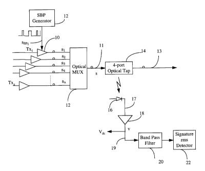
Figure 1 shows a block diagram of a WDM system using the
signature bit patterns according to the invention. The WDM system of
Figure 1 shows a plurality of optical signals s1- sn propagating in the
same direction. It is to be understood that the invention applies also to
bidirectional optical WDM systems, such as for example to
SONET/SDH 8-wavelength bidirectional systems.
Signals s1 - sn are multiplexed in an optical multiplexer 10 to
obtain a multichannel signal s on fiber 12. A signature bit pattern,
shown at sBpl, is inserted into the frame of optical signal s1. If we note
the average optical power of s1 with 'Pl', the average optical power of
sBp1 with 'PBpl', and the ratio between the powers of sBp1 and sl with
'm', we have the following relationship:


CA 02218951 1997-10-22
4
m = PBPl ~ P1 or, PgPl = m x P1 (1)
As the signature bit pattern is inserted in the frame of the digital
optical signal, ratio 'm' remains constant along the entire path. This is
however true only if either the extinction ratio for the optical signal
remains constant and known, or the extinction ratio is kept better than
an acceptable amount.
The optical signal s1 with the signature bit pattern is carried by
channel ~,1 on fiber 12, together with signals s2 - sn. A tap monitor at
some point of interest in the WDM system, noted 14 on Figure 1, taps
fiber 12 and receives a fraction of signal s, which comprises a respective
fraction of the optical signals s1- sn for all channels ~,1- ~,n. The tapped
fraction is converted to an electrical signal, shown by reference
numeral 19, by PIN diode 18 and then amplified by transimpedance
amplifier 20.
The electrical signal v at the output of transimpedance amplifier
comprises an ac and a do component. The do voltage Vd~ is a linear
combination of the individual optical signal powers:
Vd~=axPl+bxP2+cxPg+... nxPn (2)
where a, b, ... n are known calibration constants for the respective
transmission channel, and P1 - Pn are the optical powers of the
respective optical signals s1- sn.
Signal v is filtered in a band pass filter 22 for extracting the
frequencies of interest, which in this case are the component
frequencies of the signature bit pattern sBPl. A signature rms detector
24 detects the 'rmsl' of Sgp1 independent from the interferences from
the co-propagating optical signals. The signature rms detector may be


CA 02218951 1997-10-22
realized either with an analog filter with peak detect circuitry, or with a
super Nyquist sampling A/D converter and a DSP chip to implement a
digital matched filter detection.
At the frequencies of interest, the power of the signature bit
5 patterns for the other channels ~,2 to ~ is practically zero, by design, so
that the measured rmsl gives PBpl using the relation:
PBP1 = rmsl / a (3)
where 'a' is the calibration constant for channel ~,1, known. The
value of P1 can now be determined knowing m, which gives:
Pl = rmsl / m x a (4)
In a similar way, if the other signals s2 -sn have their own unique
signature pattern, or analog dither, the optical power of these signals
can be determined in the same way, as long as all the signal dithers are
designed to be independently detected from each other, for example
they are frequency division multiplexed.
An example of an implementation of the invention is the
application of the signature bit pattern of the invention to determining
the power of the bidirectional service optical channel (Bi-OSC). Bi-OSC
is a service channel that is transmitted and terminated at each optical
amplifier. This channel has a signalling rate of 9.72 Mb/s in each
direction and is Manchester encoded in order to reduce its interference
in the analog maintenance bandwidth (40 kHz) to acceptable levels.
The wavelength of the channel for one direction of transmission
is selected in the red band and for the reverse direction, in the blue
band. The frame of the signal transmitted on this channel has 2430 bits,
96 bits being used for the signature. The average optical power of the
Bi-OSC is also accounted for in order to make the average output


CA 02218951 1997-10-22
6
control in the forward direction of transmission (i.e. the red band) and
in the reverse direction of transmission (i.e. the blue band) more
accurate by subtracting the power contribution from the respective OSC
channels.
The signature bit pattern for the red channel is inserted on a
frame by frame basis. After the Manchester encoding, the red OSC
signature pattern is inserted in the following bit positions of the red
OSC frame.
Table 1. Red OSC signature bit pattern
Bit Position Red
OSC
signature
block


1 1111001111000110


401 0011110011110110


801 0011110011110110


1217 0000110000111001


1617 1100001100001001


2017 1100001100001001


The spectrum of the red OSC signature bit pattern comprises odd
multiples of 4kHz, namely 4kHz, l2kHz, 20kHz, etc. which makes it
phase orthogonal to the AM dithers, SONET 8kHz tones and the blue
signature bit pattern.
The minimum hamming distance between the first block and
the other blocks within the frame is 8.
The signature bit pattern for the blue channel is inserted on a
two consecutive frame by two consecutive frame basis. After the
Manchester encoding, the blue OSC signature pattern is inserted in the
following bit positions.


CA 02218951 1997-10-22
7
Table 2. Blue OSC signature bit pattern
Frame # Bit Position Red OSC signature block


First Frame 1 11110011 1100 0110


401 0011 11001111 0110


801 0011 110011110110


1217 1100 0011 00001001


1617 1100 0011 00001001


2017 1100 001100001001


Second Frame 1 00001100 0011 1001


401 1100 001100001001


801 1100 001100001001


1217 0011 110011110110


1617 0011 110011110110


2017 0011 110011110110


The spectrum of the blue OSC signature bit pattern are odd
multiples of 2kHz, namely 2kHz, l6kHz, lOkHz, etc. which makes it
phase orthogonal to the AM dithers, SONET 8kHz tones and the blue
signature bit pattern.
The minimum hamming distance between the first block and
the other blocks within the frame is 8.
While the invention has been described with reference to
particular example embodiments, further modifications and
improvements which will occur to those skilled in the art, may be
made within the purview of the appended claims, without departing
from the scope of the invention in its broader aspect.

Representative Drawing
A single figure which represents the drawing illustrating the invention.
Administrative Status

For a clearer understanding of the status of the application/patent presented on this page, the site Disclaimer , as well as the definitions for Patent , Administrative Status , Maintenance Fee  and Payment History  should be consulted.

Administrative Status

Title Date
Forecasted Issue Date 2004-12-07
(22) Filed 1997-10-22
(41) Open to Public Inspection 1999-04-22
Examination Requested 2000-09-28
(45) Issued 2004-12-07
Deemed Expired 2006-10-23

Abandonment History

Abandonment Date Reason Reinstatement Date
2002-10-22 FAILURE TO PAY APPLICATION MAINTENANCE FEE 2002-11-08

Payment History

Fee Type Anniversary Year Due Date Amount Paid Paid Date
Application Fee $300.00 1997-10-22
Registration of a document - section 124 $0.00 1998-05-29
Maintenance Fee - Application - New Act 2 1999-10-22 $100.00 1999-08-05
Registration of a document - section 124 $0.00 2000-02-01
Request for Examination $400.00 2000-09-28
Maintenance Fee - Application - New Act 3 2000-10-23 $100.00 2000-09-28
Maintenance Fee - Application - New Act 4 2001-10-22 $100.00 2001-10-04
Registration of a document - section 124 $0.00 2002-10-30
Reinstatement: Failure to Pay Application Maintenance Fees $200.00 2002-11-08
Maintenance Fee - Application - New Act 5 2002-10-22 $150.00 2002-11-08
Maintenance Fee - Application - New Act 6 2003-10-22 $150.00 2003-08-28
Final Fee $300.00 2004-08-25
Maintenance Fee - Application - New Act 7 2004-10-22 $200.00 2004-09-21
Owners on Record

Note: Records showing the ownership history in alphabetical order.

Current Owners on Record
NORTEL NETWORKS LIMITED
Past Owners on Record
HABEL, RICHARD A.
HARLEY, JAMES
NORTEL NETWORKS CORPORATION
NORTHERN TELECOM LIMITED
Past Owners that do not appear in the "Owners on Record" listing will appear in other documentation within the application.
Documents

To view selected files, please enter reCAPTCHA code :


To view images, click a link in the Document Description column. To download the documents, select one or more checkboxes in the first column and then click the "Download Selected in PDF format (Zip Archive)" or the "Download Selected as Single PDF" button.

List of published and non-published patent-specific documents on the CPD .

If you have any difficulty accessing content, you can call the Client Service Centre at 1-866-997-1936 or send them an e-mail at CIPO Client Service Centre.


Document
Description 
Date
(yyyy-mm-dd) 
Number of pages   Size of Image (KB) 
Abstract 1997-10-22 1 22
Description 1997-10-22 7 273
Representative Drawing 1999-05-06 1 4
Claims 1997-10-22 3 76
Drawings 1997-10-22 1 11
Cover Page 1999-05-06 1 16
Claims 2004-02-16 4 110
Representative Drawing 2004-11-03 1 6
Cover Page 2004-11-03 1 37
Correspondence 2004-01-22 2 66
Correspondence 2004-08-25 1 25
Fees 2004-09-21 1 29
Assignment 1997-10-22 3 82
Correspondence 1998-01-13 1 31
Assignment 1998-02-18 2 73
Correspondence 1998-02-18 1 39
Assignment 2000-01-06 43 4,789
Prosecution-Amendment 2000-09-28 1 34
Assignment 2000-09-28 1 30
Correspondence 2000-10-25 1 1
Assignment 2000-09-25 29 1,255
Assignment 2000-11-09 1 25
Correspondence 2000-12-01 1 24
Correspondence 2001-04-25 9 381
Correspondence 2002-10-22 1 28
Prosecution-Amendment 2003-08-18 2 37
Correspondence 2003-08-28 2 66
Correspondence 2003-09-16 1 16
Correspondence 2003-09-16 1 20
Fees 2003-08-28 1 33
Fees 2001-10-04 1 34
Fees 2002-11-08 1 35
Fees 2000-09-28 1 33
Fees 2002-10-17 1 37
Prosecution-Amendment 2004-02-18 7 203
Fees 1999-08-05 1 31
Correspondence 2004-03-15 1 16
Correspondence 2004-03-15 1 18
Correspondence 2006-01-13 2 128