Note: Descriptions are shown in the official language in which they were submitted.
CA 02219164 1997-10-24
WO 96!35272 PCTIUS96/0407:~
METHOD AND APPARATUS FOR CONTROLLING FREQUENCY
DE~~IATION OF A PORTABLE TRANSCEIVER
4
. 5
Field of the Invention
This i:nvenition relates in general to selective call communication
systems, and( more specifically to a method and apparatus for controlling
frequency deviation of a portable transceiver.
Background of the Invention
In a sE:lecti~~e call communication system modern base stations use
accurate frequency deviation modulators for transmission of hZ-ary
frequency shift .keyed (FSK) frequency modulated (FM) signal;> for
transmission of outbound messages to portable transceivers. Normally
these base stations service very large numbers of subscriber users why are
accustomed i:o low cost subscriber units providing~reliable transmission of
selective call. messages. For this reason, the . base stations use accurate
timebase systems to generate accurate frequency deviation levels during
outbound message transmission to the portable transceivers. The accuracy
of the transmiitted signals provides a means for accurate message rece~~tion
by the port~~ble transceivers with relatively inexpensive conventional
receiver hardware.
The inbound messages transmitted by the portable transceivers
provide an important means for the base stations to determine the
reliability of the message transaction. For this reason, accurate inbound
transmission is also important. Since the proliferation of portable
transceivers is much higher than that for the base stations and ;>ince
' subscriber omits are expected to be inexpensive by the common user, it is
- 30 unfeasible and too costly to consider a transmission architecture dE~sign
similar to the base stations for the portable transceivers.
~ Thus, what its needed is a cost effective method and apparatus iz1 the
portable transceiver for controlling frequency deviation levels during
~ inbound transmission while maintaining the accuracy needed for the base
stations to reliably receive the message.
CA 02219164 1997-10-24
WO 96135272 PGT/US96/04077
2
Brief Description of the Drawings
FIG. 1 is an electrical block diagram of a selective call a
communication system in accordance with the preferred embodiment of
the present invention. .
FIG. 2 is an electrical block diagram of elements of a fixed portion of
the selective call communication system in accordance with the preferred
embodiment of the present invention.
FIG. 3 is an electrical block diagram of a portable transceiver in
accordance with the preferred embodiment of the present invention.
FIG. 4 is a timing diagram of elements of an outbound protocol and
an inbound protocol of the fixed and portable portions of the selective call
communication system in accordance with the preferred embodiment of
the present invention. -
FIG. 5 is a firmware block diagram of elements of the portable
transceiver in accordance with the preferred embodiment of the present
invention.
FIG. 6 is an electrical block diagram of portions of a transceiver
element of the portable transceiver in accordance with the preferred
embodiment of the present invention.
FIG. 7 is a flow chart depicting operation of the fixed portion of the
selective call communication system in accordance with the preferred
embodiment of the present invention.
FIG. 8 is a flow chart depicting operation of the portable transceiver
in accordance with the preferred embodiment of the present invention.
FIG. 9 is a flow chart (continuation of FIG. 8) depicting operation of
the portable transceiver in accordance with the preferred and alternative
embodiments of the present invention.
Description of the Preferred Embodiment
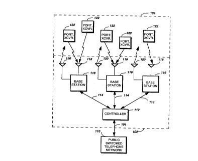
Referring to FIG. 1, an electrical block diagram of a selective call
communication system in accordance with the preferred embodiment of
the present invention comprises a fixed portion 102 and a portable portion '
104. The fixed portion 102 comprises a plurality of conventional base
transceivers which are base stations 116 coupled by communication links
114 to a controller 112 for controlling the base stations 116. The hardware
CA 02219164 1997-10-24
WO ~6I352'72 PCTYUS96/0407i
3
of the controller 112 is preferably similar to the Wireless Mess:~ging
Gateway (WMGTM) Administrator! paging control center manufactured by
~ Motorola, Inc. of Schaumburg, Illinois. The hardware of the base st~itions
116 is preferably similar to the NucleusTM Orchestra! manufactured by
Motorola, Inc. off Schaumburg, Illinois. Other similar controller hardLware
can be utilized as well for the controller 112 and base stations 116. The
controller 11.2 comprises a plurality of firmware elements in accordance
with the .preferred embodiment of the present invention, as will be
described further below.
Each of the base stations 116 transmits radio signals to the portable
portion 104 comprising a plurality of portable transceivers 122 via a
transmitting antenna 120. The base stations 116 each receive radio signals
from the plurality of portable transceivers 122 via a receiving antenna 118.
The radio ;signals comprise selective call addresses and messages
transmitted to the portable transceivers 122 and acknowledgments
received from the portable transceivers 122. It will be appreciated that the
portable transceivers 122 can also originate messages other than
acknowledgments. The controller 112 preferably is coupled by teleyhone
links 101 to the public switched telephone network (PSTN) 110 for
receiving selective call originations therefrom. Selective call origina.tions
comprising voice .and data messages from the PSTN 110 can be generated,
for example, from. a conventional telephone coupled to the PSTN 11(I in a
manner that is well known in the art.
Data a:nd control transmissions between the base stations 116 and the
portable transceivers 122 preferably utilize a well-known digital selective
call signaling; protocol, such as the Motorola ReFLEXTM protocol. It will be
appreciated that other protocols such as Motorola's new FLEXTM and
InFLEXionTM protocols can be utilized as well. These protocols utilize
well-known error detection and error correction techniques and are
therefore tolerant to bit errors occurring during transmission, provided
that the bit e~crors are not too numerous in any one code word.
Outbound channel transmissions comprising data and control
signals from the base stations 116 preferably utilize four-level frequency
shift keyed (IRSK) modulation, operating at sixteen-hundred or thirty--two-
hundred symibols-per-second (sps), depending on traffic requirement~~ and
system tran:>mission gain. Inbound channel transmissions from the
portable transceivers 122 to the base stations 116 preferably utilize binary
CA 02219164 2000-06-06
i
W O 96!35272
PCTlUS96/040T7
Q
FSK modulation at a rate of ninety-six-hundred bits per second (bps).
Inbound dzannel transmissions preferably occur during predetermined
data packet time slots synchronized with the outbound channel
transmissions. It will be appreciated t~~.at, alternatively, other signaling
protocols, modulation schemes, and transmission rates can be utilized as
well for either or both transmission directions. The . outbound and
inbound channels preferably operate on a single carrier frequency utilizing
well-known time division . duplex (TDI7) techniques for sharing the
frequency. ~ '
I0 U.S: Patent No. 4,875,038 to Siwiak et al., desan'bes a prior art
acknowledge-back selective _ call communication s~rstem_
For further information on the
o~pei~ation and. ~ structure of , an acknowledge-back selective call
communication system, please, refer to the Siwiak et al. patent
Referring to FIG. 2, an electrical block diagram of elements 200 of the .
fixed portion I02 in accordance with the preferred embodiment of the
present invention comprises portions of the controller lI2 and the base
stations 116. The controller 112 comprises a control processor~2l2.for.
w directing operation of the controller II2. The control processor ZIZ
preferably is coupled through, a transmitter .interface SOS to a transmitter
202, both utilizing conventional techniques well known in~ the ait_ The .
transmitter.202 preferably transmits four-Ievel FSK data messages to one of
~e portable transceivers 122_ The control processor 212 is also coupled to
at Ieast one acknowledgment receiver 206.using conventional binary FSK
demodulation. The aclrnowledgment receiver 206 can be collocated with
. , the base stations 1~6, as implied in FIG,. 2, but preferably is positioned
remote from the base stations 116 to avoid inteFference from the
- , .transmitter ZOZ The aclatowledgment receiver 206 is. for receiving one or
more aclmoyvledgmenfis from the plurality portable transceivers I22
The control processor ZI2 is coupled, to a random access memory
(RAM) 210 for storing messages to be transmitted to the portable
transceivers 122; and for. stoiing~ messages received from the poitable
' ~ ~ .transceivers I22_ ' The control processor 2I2 also, is coupled to a
read-only '
memory (ROM) 214 comprising firmware elements for-use by the control
~ processor 2I2. It will be appreciated that other types of memory. e.g..
electrically erasable programmable ROM (EEPROM) or magnetic disk
memory, can be utilized as well for the. ROM 214 or RAM ZIO. It will be
CA 02219164 1997-10-24
WO 96!35272 ' PGT/US96/04077
further appreciated that the RAM 210 and the ROM 214, singly or in
combination, can be integrated as a contiguous portion of the control
processor 2.12. Preferably, the control processor 212 is similar i:o the
DSP56100 digital signal processor (DSP) manufactured by Motorola, :fnc. of
. 5 Schaumbur~;, IL. It will be appreciated that other similar processors <=an
be
utilized as well for the control processor 212, and that additional processors
of the samE~ or alternate type can be added as required to handle the
processing requirements of the controller 112.
The firmware elements comprise a call processing element 21'8 for
handling th.e processing of an incoming call for a called party and for
controlling the transmitter 202 to send a message identifying the call
source to tree portable transceiver 122 corresponding to the called party,
utilizing te~chniclues well known in the art. The firmware elements
further comprise. a frequency deviation generator 220 further comprising a
1:i first sender element 222, a second sender element 224, a third sender
element 22Ei and': a fourth sender element 228, in accordance with the
preferred ernbod:iment of the present invention. The first sender element
222 is used by the control processor 212 as a means for sending a
predetermined signal to the base stations 116 via the communication links
114 having a predetermined plurality of frequency deviation levels. The
predetermined signal is used by the precision frequency deviation
modulator 204 for transmitting a signal to the portable transceivers 12;2.
The seconds sender element 224 is used by the control processor 212
as a means for transmitting from the base stations 116 a predetermined
25~ signal having N predetermined frequency deviation levels, N being a
predetermined iinteger, and wherein the second modulated ~~ignal
transmitted by the portable transceiver 122, as will be described fixrther
below, has Dn frequency deviation levels, M being a predetermined ixiteger
greater than N. hor example, for N equal to two and M equal to four, the
base station:> 116 transmit two level FSK and the portable transceivEsr 122
transmits a ~~econd modulated signal using four level FSK.
In an alternative embodiment of the present invention, the third
sender element 226 is used by the control processor 212 as a means for
transmitting frown the base stations 116 a predetermined signal having N
predetermined frequency deviation levels, M of which correspond t:o the
M frequency deviation levels of the second modulated signal transmitted
by the portahle transceiver 122, N being a predetermined integer equal to or
CA 02219164 1997-10-24
WO 96135272 - PGT/US96/04077
6
greater than M. For example, for N equal to four and M equal to two, the
base stations 116 transmit four level FSK and the portable transceiver 122
transmits a second modulated signal using two level FSK. Similarly, for N ,
equal to four and M equal to four, the base stations 116 and the portable
transceiver 122 transmit the same number of frequency deviation levels, ,
that is, both transmit four level FSK. The significance of the second sender
element 224 and third sender element 226 will become evident in the
discussion of the firmware elements of the portable transceiver 122, and in
particular a discussion of the comparator element 524 of FIG. 5, as will be
described further below.
The fourth sender element 228 is used by the control processor 212 as
a means for transmitting from the base stations 116 a predetermined signal
having N predetermined frequency deviation levels, N being a
predetermined integer, and wherein ones of the N predetermined
frequency deviation levels are transmitted a plurality of times in the
predetermined signal. In processing a received message from the PSTN
110 the fixed portion 102 of the selective call communication system
generates a signaling format enabling communication with the portable
transceiver 122. In the message signaling format an outbound preamble
406 (FIG. 4) is transmitted by the base stations 116. The outbound
preamble 406 is used by the portable transceiver 122 for both signal
synchronization, and for deriving frequency deviation level references to
be later used during inbound transmission. The frequency deviation
references are used as a means for determining the accuracy of the second
modulation signal transmitted by the portable transceiver 122, as will be
described further below.
Referring to FIG. 3, an electrical block diagram of the portable
transceiver 122 in accordance with the preferred embodiment of the
present invention comprises a transceiver antenna 302 for transmitting
and intercepting radio signals to and from the base stations 116,
respectively. The radio signals linked to the transceiver antenna 302 are
coupled to a transceiver 304. The radio signals received from the base
stations 116 use conventional two and four-level FSK. Similarly, radio
signals transmitted by the transceiver 304 to the base stations 116 also use '
two and four-level FSK. It will be appreciated by one of ordinary skill in
the art that the transceiver antenna 302 is not limited to a single antenna
for transmitting and receiving radio signals. Separate antennas for
CA 02219164 1997-10-24
WO !96/35272 ~ FCTlUS961040Z'~
receiving and transmitting radio signals would also be suitable. The radio
signals just ~3iscu;ssed are preferably selective call (paging) signals which
use ReFLEXTM signaling formats. It will be appreciated that other sigr~aling
formats can also be used.
Radio signals received by the transceiver 304 produce demodulated
information at the output. The demodulated information is
transferred
over a signal information bus 305 which is coupled to the
input of a
processor 308, which processes the information in a manner
well known
- in the art. Similarly, acknowledge response messages are
processed by the
processor 308 and delivered through the signal information
bus 305 to the
transceiver 304. The acknowledge response messages transmitted
b:y the
transceiver 304 are preferably modulated using two and four-level
FSK
operating at a bit rate of ninety-six-hundred bps. It will
be appreciated that
other bit rate;a can be used as well.
A conventional power switch 306, coupled to the processor
308, is
used to control ithe supply of power to the transceiver 304,
thereby
providing a battery saving function. The processor 308 is
coupled to a
random access memory (RAM) 322 for storing messages in a
me~~sage
storage location 324 and a present control signals element
33(1 for
processing of the second .modulated signal. The processor
308 is also
coupled to an electrically erasable programmable read only
memory
(EEPROM) 321 which comprises a frequency deviation level
referE~nces
element 323, an adjustment control signal values element
326 and a
- default adjustment control signal values element 328. The
EEPROlNt 321
serves as a non-volatile memory device for storing the reference
elements
used for processing the second modulation signal, as will
be described
below. The processor 308 also is coupled to a read-only memory
(ROM) 310
comprising fiirmware elements for use by the processor 308.
It will be
appreciated that other types of memory, e.g., electrically
erasable
programmable ROM (EEPROM), can be utilized as well for the
ROM 3:L0 or
RAM 322.
' The firmware elements comprise a call processing element
311
further comprising; a selective call address 312 for handling
of incoming
messages on the outbound channel using techniques well known
im the
art. When an address is received by the processor 308, the
call proce~~sing
element 311 comb>ares one or more selective call addresses
312 stored in
ROM 310, and when a match is detected, a call alerting signal
is generated
CA 02219164 1997-10-24
WO 96135272 ~ PCT/US96/04077
8
to alert a user that a message has been received. The call alerting signal is
directed to a conventional audible or tactile alerting device 318 for
generating an audible or tactile call alerting signal. In addition, the call
processing element 311 processes the message which is received in a
digitized conventional manner and then stores the message in the .
message storage location 324 in RAM 322. The message can be accessed by
the user through user controls 316, which provide functions such as lock,
unlock, delete, read, etc. More specifically, by the use of appropriate
functions provided by the user controls 316, the message is recovered from
the RAM 322, and then displayed on a display 320, e.g., a conventional
liquid crystal display (LCD).
The firmware elements further comprise a frequency deviation
determinator element 314 used by the processor 308 during acknowledge
response messaging for determining the frequency deviation levels to be
used for accurate transmission to the base stations 116, in accordance with
the preferred embodiment of the present invention. Once the frequency
deviation levels have been determined by the frequency deviation
determinator element 314, the processor 308 invokes an acknowledge-back
transmission element 315 which controls transmission of the acknowledge
response message to the base stations 116.
Referring to FIG. 4, a timing diagram depicts elements of an
outbound protocol and an inbound protocol of the fixed portion 102 and
portable portion 104 of the selective call communication system in
accordance with the preferred embodiment of the present invention. The
signaling format operating on the outbound and inbound channels
preferably operates on a single carrier frequency utilizing well-known time
division duplex (TDD) techniques for sharing the frequency. Using TDD
transmission the outbound RF channel transmission is depicted as an
outbound transmission time interval 402, while the inbound RF channel
transmission is depicted as an inbound transmission time interval 404.
The outbound transmission time interval 402 and the inbound
transmission time interval 404 are subdivided by a time boundary 403.
The time boundary 403 depicts a point in time when the outbound
transmissions cease and the inbound transmissions commence. '
' The elements of the outbound protocol comprise an outbound
preamble 406, a selective call address 408, a message vector 410 and a
message 412, while the inbound protocol comprises an inbound preamble
CA 02219164 1997-10-24
w0 X6135272 ~ PCTlUS96f040?'7
9
414 and an acknowledge-back message 416. The outbound preamble 406
would preferably consists of a recognizable pattern such as an alternating
binary one's .and z;ero's pattern. It will be appreciated, however, that ether
patterns whinh exercise all four frequency deviation levels can be utilized
a 5 for the preamble. The outbound preamble 406 is used by the portable
transceiver 122 for measuring frequency deviation levels received on the
outbound channel.. The selective call address 408 identifies the portable
transceiver 122 which the message 412 is intended. The message vector 410
points in time within the TDD signal format to the position of the me~~sage
412 to be received by the portable transceiver 122. Similarly, the inbound
preamble 41~t preferably consists of a recognizable pattern such as an
alternating binary one's and zero's pattern. It will also be appreciated that
other patterns which exercise all four frequency deviation levels can be
utilized. They inbound preamble 414 transmitted on the inbound channel
forms the second modulated signal which the portable transceiver 122
uses, in conjjunctiton with either the adjustment control signal values
element 326 or the default adjustment control signal values element 328,
for adjustment of the transmission signal to match the transmission
reference of the base stations 116, as will be discussed below.
Referral g to FIG. 5, a block diagram depicting the firmware elements
of the frequency deviation determinator element 314 of the portable
transceiver 122 in accordance with the preferred embodiment of the
present invention comprises a measurement element 510, a sampler
element 520, an appraiser element 522, a comparator element 524, a
deviation control element 532, a reversion control element 534 and a
defaulter control element 536. As shown, the measurement element 510
comprises an instantaneous determination element 512, a calculation
element 514, ;gin evaluation element 516 and a derivation element 518.. In
addition, the comparator element 524 comprises a first control si;~nal
element 526, an interpolation element 528 and a second control si;~nal
element 530. The second control signal element 530 is an alternative
embodiment in accordance with the present invention and is highlighted
with dashed limes for this reason.
' When the base stations 116 transmit the outbound preamble 406,, for
example, in two and four level FSK to the portable transceiver 122, the
transceiver 304 demodulates the received signal to baseband and provides
the demodulai:ed information in a binary digitized format to the processor
W O 96/35272 CA 0 2 21916 4 19 9 7 -10 - 2 4 p~~S96/04077
308. Each binary sample represents symbol levels from a predetermined
symbol alphabet. The measurement element 510 derives frequency
deviation level references from the outbound preamble 406. The .
alternating pattern incorporated in the outbound preamble 406 preferably
5 exercises two predetermined frequency deviation levels, which the
instantaneous determination element 512 uses for measuring two
pluralities of instantaneous deviation levels. The calculation element 514
then calculates two mean values corresponding to the two pluralities of
instantaneous deviation levels. The evaluation element 516 determines
10 the signal integrity of the outbound message by evaluating the first
received signal to produce an error count of errors received in the first
received signal. A quality test is performed by the evaluation element 516
to determine if the error count has exceeded a predetermined error
threshold such as, for example, one uncorrectable bit error. It will be
appreciated that other methods may be utilized, such as correlation
between the received preamble and the known bit pattern of the preamble.
The error detection and correction mechanism is preferably implemented
with a coding scheme such as Bose, Chaudhuri, Hocquernghem (BCH), as
is well known by one of ordinary skill in the art. It will be appreciated that
other error detection and correction codes can be used. If the quality test is
passed, the derivation element 518 derives estimates of the frequency
deviation levels of the outbound preamble 406. The estimates determined
by the derivation element 518 preferably are the two mean values
generated by the calculation element 514. It will be appreciated that other
forms of estimates can be used, for example, a single instantaneous
sampling of the two predetermined frequency deviation levels. After the
measured frequency deviation levels have been processed, the
measurement element 510 stores the results in the frequency deviation
level references element 323 in the EEPROM 321.
Before the acknowledge-back transmission element 315 is invoked,
the frequency deviation determinator 314 begins inbound channel
processing and adjusts the inbound transmission circuits for acknowledge-
back messaging. During inbound transmission the frequency deviation
determinator 314 begins transmitting a second modulated signal '
comprising the inbound preamble 414. The signal transmitted has enough
power density to be RF coupled into the receiver circuits. The receiver
circuits demodulate the signal in the same manner as with outbound
CA 02219164 1997-10-24
~'O :96/35272 ' PCT/US961040T7
11
messages. The demodulated information, as before, is in a binary digitized
format delivered to the processor 308. The binary digitized format is used
by the sampler element 520 to create a second receive sigma for
comparison to the frequency deviation level references 323 pre-stored in
EEPROM 32:L. 'The appraiser element 522 appraises the second received
signal to derive estimates of the second plurality of ffrequency deviation
levels.
The co~mparator element 524 compares corresponding estimates of
the first and second pluralities of frequency deviation levels to derive a
plurality of adjusted control signal values for controlling the second
plurality of frequency deviation levels. In a preferred embodiment c~f the
present invention, the comparator element 524 uses a first control signal
element 526 for derivation of the four frequency deviation levels needed
for inbound channel transmission. In this embodiment, the second
modulated signal transmitted by portable transceiver 122 preferably has
four frequency deviation levels which exceed the two frequency deviation
levels transmitted by the base stations 116. The first control signal element
526 compare;> two of the frequency deviation level references element 323
stored in EEI'ROl~'I 321 with two corresponding frequency deviation levels
of the second modulated signal to derive two adjusted control signal
values for controlling the two corresponding frequency deviation levE~ls of
the second modulated signal. Since the portable transceiver 122 needs four
frequency dcwiation levels for transmission to the base stations 116, a
mechanism is needed to derive the two remaining frequency deviation
levels for acl;now:ledge-back transmission. The interpolation element 528
interpolates Hetwe~en the two adjusted control signal values to obtain two
additional adjusted control signal values corresponding to the two
additional frequency deviation levels of the second modulated signal.
Once the two additional frequency deviation levels have been determined,
all four frequency deviation levels have been derived and acknowlE~dge
back transmission deviations can be adjusted accordingly. It will be
' appreciated that other symbol alphabets can be utilized, for example, eight
level, sixteen level FSK, etc.
In an alternative embodiment of the present invention, the
comparator element 524 uses a second control signal element 530 for
derivation of M .frequency deviation levels needed for inbound channel
transmission. In this embodiment, the N frequency deviation levels
CA 0 2 21916 4 19 9 7 - 10 - 2 4 pL-L~s96/04077
WO 96135272
12
transmitted by the base stations 116 exceed or equal the M frequency
deviation levels transmitted by portable transceiver 122 . In this case, the
second control signal element 530 is compared to M of the frequency -
deviation levels stored in the frequency deviation level references element
323 with M frequency deviation levels of the second modulated signal to 9
derive M adjusted control signal values.
TABLE 1
First Second Error betweenPresent New adjusted control
values
receivedreceivedfirst receivedsecond based on calculated
error
signal signal signal modulationwhich will replace
the
digitizeddigitizedreferences signal present second modulation
and
frequencyfrequencysecond modulatedadjustedsignal adjusted control
deviationdeviationsignal digitizedcontrol values
level levels samples values
references
Vh Vw Eh = Vh - Va Vanew =
Vw
Va + Eh * K
Vmh Vx Emh = Vmh Vb Vbnew =
- Vx
Vb + Emh * K
Vml Vy Eml = Vml Vc Vcnew =
- Vy
Vc + Eml * K
VI Vz EI = VI - ~l Vdnew =
Vz
Vd + EI * K
TABLE 1, shown above, summarizes the preferred calculation
process for the comparator element 524 described above. As discussed
above, in the preferred embodiment in accordance with the present
invention, the portable transceiver 122 receives two frequency deviation
levels from the base stations 116 preferably using two level FSK. The
receiver hardware, to be described below, demodulates the outbound signal
to baseband and generates binary digitized samples in the form of a voltage
level symbol alphabet. The plurality of digitized samples constitutes two
frequency deviation levels of the first received signal. The measurement
element 510 processes and stores estimates of the digitized samples in the
frequency deviation level references element 323 in the EEPROM 321. The
estimates stored in the frequency deviation level references element 323
closely match the frequency deviation levels transmitted by the base
stations 116. For two level FSK, TABLE 1 represents the two level
estimates stored in the frequency deviation level references element 323 by
the values Vh (voltage high) and Vl (voltage low) shown in the first
CA 02219164 1997-10-24
WO X6/35272 PCTlUS96/040T1
13
column of the table. The values Vmh (voltage medium high) and Vml
(voltage medium low) are used when the outbound signal is transmitted
- with four level F;3K, which applies to the alternative embodiment of the
present invention, to be discussed below.
. 5 During inbound transmission the inbound preamble 4~i4 is
transmitted in a second modulation signal which RF couples to the
receiver circuits and is demodulated in the same format the outb ound
signal was demodulated. Since Vh and Vl are the only frequency
deviation re:Eerences available from the base stations 116, the frequency
deviation de~termi:nator 314 generates the second modulated signal with an
attempt to match Vh and Vl. At start-up the default values stored in the
adjusted control signal values element 328 are utilized. The binary
digitized sarrtples generated by the receiver circuits are used by the sampler
element 520 to <:reate a second receive signal for comparison to the
frequency deviation level references element 323 represented by Vr~ and
Vl. The aphraisE~r element 522 appraises the second received signal to
derive digiti:aed estimates of the frequency deviation levels of the second
received signal. TABLE 1 represents the two digitized frequency deviation
levels generated by the appraiser element 522 as the values Vw and Vz.
The values 'Vx and Vy are used when the second modulated signal is
transmitted with. four frequency deviation levels. The comparator
element 524 calculates the difference between Vh and Vw, and Vl anal Vz
to determine the digital error present in the second received signal.
TABLE 1 shows the error between Vh and Vw by the equation Eh and the
error between Vl ;end Vz by the equation El. The fourth column of Tr~BLE
1 shows they present adjusted control values which are stored in the
present control signal element 330 in RAM 322 used by the frequency
deviation determinator 314 to control the second modulated signal. The
values Va and Vd are the present estimates used for controlling the second
modulated signal, which generate Vw and Vz, respectively in an attempt
to match Vh and 'Vl, respectively.
The fifth column of TABLE 1 shows the new adjusted control values
based on the calculated error, which will replace the present second
modulation ;signal adjusted control values in the fourth column. 7Chese
new values a.re determined by multiplying the digital error (Eh or El) with
the gain Kp of the processor 308. The circuit loop used for adjusting the
second modmlatio~n signal includes a transmitter block, a receiver block,
CA 02219164 1997-10-24
WO 96135272 PCT/US96/04077
14
both to be described in detail below, and the processor 308. Kp represents
the loop gain of the processor 308 used for adjusting the control values of
the second modulation signal. The transmitter block has a gain factor to
be denoted by Kt and the receiver block also has a gain factor to be denoted
by Kr. The transmitter block converts volts to frequency based on the
input voltage provided (i.e., Va through Vd and corresponding to Fa
through Fd), while the receiver block converts frequency to voltage based
on the input frequency provided (i.e., Fa through Fd and corresponding to
Vx through Vz). The overall system gain is Ks which equates to the
product of Kp, Kt and Kr. In order for the system to remain stable, Ks must
be less than unity and is preferably in the range of 0.2 to 0.5. Kt and Kr are
preferably constant values and are determined from design of the
conventional transmitter and receiver blocks. Kp is chosen appropriately
to maintain the system gain Ks less than unity and preferably in the range
of 0.2 to 0.5.
To calculate the value of Vanew which correspondingly updates Va,
the digital error Eh is multiplied by Kp. This factor gives the number of
increments (positive or negative) needed for adjusting the present
adjustment value Va. Once Vanew is calculated it serves as the new
adjustment level used by the frequency deviation determinator 314 for
transmitting the second modulated signal controlled by Va. The value
Vdnew which is adjusted to match Vl is calculated in the same manner.
The adjustment process for Vanew and Vdnew ceases when the
incremental adjustments oscillate between plus or minus one bit change
from the present values of Va and Vd, respectively. It will be appreciated
that other comparison methods for the determination of the second
modulated signal adjustment values Va and Vd can be utilized.
Once Va and Vd adjusted have been calculated, the values Vb and
Vc must be calculated by the interpolation element 528. The relationship
of voltage to frequency is preferably linear; thus by knowing Va relative to
a frequency Fa and Vd relative to a frequency Fd the slope of the frequency
versus voltage line can be determined. The slope m thus equals to (Fd -
Fa) / (Vd - Va), i.e., the ratio of the difference between Fd and Fa to the
difference between Vd and Va. By knowing the slope m the values Vb at a
desired frequency Fb and Vc at a desired frequency Fc can be determined.
For example, with the equation m equals (Fa - Fb) / (Va - Vb), Vb can be
solved for easily since Vb is the only unknown variable. Similarly, Vc can
CA 02219164 1997-10-24
WO 96/35272 PCTIUS96I04077
be solved from m equals (Fd - Fc) / (Vd - Vc). It will be appreciated b;y one
of ordinary ;>kill iin the art that other more sophisticated methods c~~n be
- utilized. For example, when the transceiver circuit behavior indicates a
non-linear frequency to voltage relationship, a characterization curve can
. 5 be programnned into each portable transceiver 122 during manufactmring.
The pre-prograin.med characterization curve may be used durin~~ the
interpolation process to determine values such as Vb and Vc.
In an alternative embodiment in accordance with the present
invention the outbound signal has equal or greater frequency deviation
10 levels to the second modulated signal sent during inbound transmi~>sion.
In this case, the :interpolation element 528 is not necessary. Instead all
levels used i:n the second modulation signal are determined directly in the
same manner as V'a and Vd, as described above.
Once all inbound transmission adjustment control values have
15 been determined (e.g., Va, Vb, Vc and Vd) these values are stored in the
adjustment ~~ontrol signal values element 326. The deviation ccmtrol
element 532 use;> the values in the adjustment control signal values
element 32E~ to control the transmitter hardware, to be described below,
which transmits the acknowledge-back message in four level FSK tuned to
the frequency deviation levels of the base stations 116.
When the evaluation element 516 determines the outbound
received sigxial inaegrity does not meet the necessary quality thresholds,
the compara~tor element 524 is bypassed. Thus, the calculations described
above are bypass<~d, and the reversion control element 534 is invokf~d by
the processor 308. Since the comparator element 524 is bypassed the
reversion control element 534 reverts to the adjustment control signal
values element 326 stored in the EEPROM 321 processed from a previous
adjustment control process during inbound channel transmission. If,
however, the rEwersion control element 534 determines that the
adjustment control signal values element 326 does not contain pre-stored
adjusted control signal values, the defaulter control element 536 is
invoked. The defaulter control element 536 reverts to the default
adjustment control signal values element 328. pre-stored in EEPROM: 321.
The values in the default adjustment control signal values element 328 are
preferably deterin.ined during the manufacturing process of the portable
transceiver 122, and in particular during RF tuning of the transceiver 304
hardware. It will be appreciated that the values in the default adjustment
CA 02219164 1997-10-24
WO 96135272 PCT/US96/04077
16
control signal values element 328 can, alternatively, be derived by periodic
sampling of outbound adjustment frames transmitted by the base stations
116 or by other related methods.
Referring to FIG. 6, an electrical block diagram of the hardware of
the transceiver 304 in accordance with the preferred embodiment of the -
present invention comprises a receiver portion 601 and a transmitter
portion 602. The transceiver antenna 302 is coupled to an RF switch 624
which switches between the receiver portion 601 and the transmitter
portion 602. When outbound messages are received, the RF switch is
switched to the receiver portion 601 and when inbound messages are to be
transmitted, the RF switch 624 is switched to the transmitter portion 602.
Outbound messages received by the transceiver antenna 302 are transferred
over an RF signal bus 603 coupled to the input of a conventional receiver
front end mixer 604 utilizing techniques well known in the art. The
output of the conventional receiver front end mixer 604 is coupled to an
intermediate frequency (IF) signal bus 606. The IF signal bus 606 is coupled
to the input of a conventional RF demodulator 608 which demodulates
the IF signal utilizing techniques well known in the art. The conventional
RF demodulator 608 comprises an RF discriminator 610 utilizing
conventional techniques well known in the art, which converts baseband
frequency signals to voltage symbol levels, as is well known by one of
ordinary skill in the art. The voltage symbol levels are transferred through
a baseband signal bus 612 (depicted with symbol wave forms by way of
example) to the input of an analog to digital converter (A/D) 614 of
conventional design well known in the art. The A/D 614 samples the
voltage level symbol alphabet on the baseband signal bus 612, generating a
binary digital representation of the symbol levels. The accuracy of the
digitized samples depends on the resolution (e.g., 8 bit A/D) of the A/D as
is well known in the art. The output of the A/D 614 is coupled to the
signal information bus 305 which transfers the digitized samples to the
processor 308. Once the digitized samples have been received by the _
processor 308 the frequency deviation determinator element 314 performs
the necessary processing to determine frequency deviation level references
as was described above.
The transmitter portion 602 receives its input from the processor 308
through the signal information bus 305. The processor 308 relays binary
digitized samples to the digital to analog converter (D/A) 616, which
CA 02219164 1997-10-24
WO 96/35272 PGTI(1S96/040T7
17
converts the digitized samples into a voltage level symbol alphabet. The
voltage level symbol alphabet is transferred on a baseband transmitter
- signal bus 61:7 (depicted with symbol wave forms by way of example) to a
voltage controlled synthesizer 618 utilizing conventional techniques well
known in they art, which modulates the voltage-level symbol alphabet to
~r r.I~~. FSI;- ~ ~. ~ ~ ......L_:_____ " ,
y , sig"m.ai, uuliziWg ~Cmuuc~uC~ welt if35owTI IIl tlTe arI. The F51~
signal generai:ed by the voltage controlled synthesizer 618 is then amplified
by a power amplifier 620 utilizing conventional techniques well known in
the art, coupled to the transceiver antenna 302, which reliably transmits an
inbound message for the base stations 116. The 1ZF signal power generated
by the power amplifier 620 is sufficient to couple enough RF energy
between the t~ransiztitter portion 602 and the receiver portion 601. It vial
be
appreciated that the RF coupling can easily be accomplished by way of a
trace on the printed circuit board of the receiver portion 601. It will also
be
appreciated that, alternatively, if the transceiver antenna 302 v~ere
composed of separate transmitter and receiver antennas, the receiver
antenna could remain connected at all times whereby the RF si~~nal
transmitted b~,~ the transmitter portion 602 would couple into the receiver
antenna. By 1ZF coupling from the transmitter portion 602 to the receiver
portion 601 the second modulated signal can be sampled and processed by
the frequency deviation determinator 314, which will generate therefsrom
the necessary frequency deviation level adjustments for transmitting; an
accurately deviated inbound channel signal.
Referring to FIG. 7, a flow chart 700 summarizing the operation of
the fixed portion 102 of the selective call communication system, in
accordance with thf~ preferred embodiment of the present invention bei;ins
with step 702 where the controller 112 receives a selective call message
from the PSTiv1 lliD. In step 704 the controller 112 sends an outbound
signaling format as described in FIG. 4 to the precision frequency deviai:ion
modulator 204 of th.e base stations 116. In step 706 the precision frequency
deviation modlulator 204 which modulates the outbound message into a
first modulation signal with N deviation levels. In step 708 the first
modulated signal is then transmitted to the portable transceiver 122. In
step 710 the bzise stations check for an acknowledgment response from the
portable transceiver 122. If an acknowledgment response is received then
the base stations 21.6 have completed the message transmission task. If,
however, no acknowledgment is received from the portable transceiver
CA 02219164 1997-10-24
WO 96!35272 PGT/US96/04077
18
122 then in step 712 a resend count is checked. If the resend count is not
exceeded re-transmission of the selective call message is restarted. If,
however, the resend count is exceeded the message transmission task is
terminated.
Referring to FIG. 8, a flow chart 800 summarizing the operation of '
the portable transceiver in accordance with the preferred embodiment of
the present invention begins with step 802 where the portable transceiver
122 receives the first modulated signal with N predetermined frequency
deviation levels sent by the base stations 116. In step 804 the first received
signal is demodulated by the receiver portion 601. In step 806 the RF
discriminator 610 generates N frequency deviation levels which are
sampled by the A/D 614. In step 808 the instantaneous digitized samples
from the A/D 614 are read by the processor 308. In step 810 mean values
are calculated for the digitized N frequency deviation levels. In step 812
the decoded message is stored in the message storage location 324 in RAM
322. In step 814 the evaluation element 516 determines the amount of
errors detected in the outbound preamble 406. It will be appreciated that
other portions of the message can also be used for error detection. In step
816 if the quality test of the evaluation element 516 fails then in step 818
the reversion control element 534 checks for pre-stored values in the
adjustment control signal values element 326 in the EEPROM 321. If pre-
stored values are not available in the adjustment control signals values
element 326 then in step 822 the defaulter control element 536 reads pre-
stored values in the default adjustment control signal values element 328
in the EEPROM 321. If, however, the reversion control element 534
determines pre-stored are available in the adjustment control signals
values element 326 then in step 820 the reversion control element 534
reads the values in the adjustment control signals values element 326.
Invocation of either the reversion control element 534 or the defaulter
control element 536 leads to step 828 to be discussed below. If the
evaluation element 516 passes the quality test in step 816 then in step 824
the derivation element 518 derives estimates from the N frequency
deviation levels using mean values calculated by the calculation element ,
514 or other comparable methods. In step 826 the estimates are stored in
the EEPROM 321. In step 828 the acknowledge-back transmission element
315 processes the acknowledge-back message. In step 830 the acknowledge-
back message is transmitted by the transmitter portion 602 in a second
CA 02219164 1997-10-24
WO 96/35272 PCTlUS96lU4U7;~
19
modulation format with M deviation levels. In step 832 the recE~iver
portion 601 receives and demodulates the second modulated signal and
the sampler element 520 samples the inbound preamble 414.
Referring to FIG. 9, a continuation flow chart 900 of FIn. 8
summarizing the operation of the portable transceiver in accordance with
the preferred and alternative embodiments of the present invention
begins with step 902 where the derivation element 518 derives frequency
deviation level estimates from the second modulated signal. In step 904 if
the M frequE~ncy deviation levels is greater than the N predetermined
frequency deviation levels sent by the base stations 116, step 906 is invoked;
otherwise step 91C1 is invoked by the processor 308. In step 906 the first
control signal. element compares the N predetermined frequency deviation
levels with rJ corresponding deviation levels sampled from the second
modulated signal to derive N adjusted control signal values. In step 908
the interpolation element 528 interpolates between the N adjusted control
signal values to oI>tain M - N additional control signal values resulting in
M total frequency deviation levels derived for acknowledge-lback
transmission. Step 910, in accordance with an alternative embodiment of
the present irmenti.on, handles .the case when M is equal to or less than N.
In step 910 the second control signal element 530 compares M
predetermined frequency deviation levels with M corresponding
deviation levels sampled from the second modulated signal. In step 912
all M adjusted control signal values are derived directly for acknowledge-
back transmission without interpolation. Both step 908 and step 912 merge
with step 914. In step 914 the deviation .control element 532 adjust~~ the
transmitter portion 602 in accordance with the adjusted control signal
values determined in the above steps. In step 916 acknowledge-.back
transmission is completed.
Thus, i.t should be apparent by now that the present invention
provides a method and apparatus for controlling frequency deviation
_ levels of a portable transceiver 122 in a cost effective manner without
sacrificing accuracy for reliable inbound communication with the base
stations 116.
What i~~ claimed is: