Note: Descriptions are shown in the official language in which they were submitted.
CA 02219266 1997-10-23
.
QPSK MODULATED BACKSCAl[TER SYSTEM
Related AI~ n
Related subject matter is disclosed in the following appllication filed
5 concurrently hc.e~.i~ and assi~ed to the same ~cci~npe hereof: U.S. patent
application~, "Shielding Technology In Mo~ te~ R~ Syctem", Serial No.
"Encrpytion for Mo~ ted R~cL ceattP Systems", Serial ~o.
",~nt~nn~ Array In An RDID System", Serial No. ; "Modulated B~ xr~
Location System," Serial No. ; "Mo~l..l~t~ R?(cL~c;~lt., Sensor System",
10 Serial No. ; "Subcarrier Frequency Division ~ulhpleYing Oi' Mod~ te~i
R~eL~ic~ll- - Signals", Serial No. ; "IQ Combiner Te~ gy ~ MC~ t~
R~Lrxc~.. System", Serial No. ; "In-Builting Personal Pager And
ntifi~", Serial No. ; "In-Building Modu~ated Ra~ t~ . System", Serial
No. ; ~r,~ re Mo~ t~t~ R~L~h ~ RPfl~c~r", Serial ~o.
15 "P~cs~ng-or~ R~gg~ge And Cargo Reconcili~tion System", Serial ~rO.
Related subject matter is also ~ elosed in the following ~pliç~tionC ~csign~ to the
same ~CCign~e hereof: U.S. patent applic~tion 08/504188, entitled "Modulated
Rz~-~L ~.r,.l l~, C~ ;cations System Having An F~ ..d~l Range"; U.S. PatentApplication Senal No 08/492,173, Pntitled "Dual Mode Mochll~t~Pl Ra~
Sya~tem~; U.S. Patent Application Seria} No. 08/4C92,174, entitled "~ull Duplex
Modulated Ra~L ~ , System"; and U.S. Patent Applic~hon Serial No. 08/571,004,
~rltitled ''F~nhz~ncp~l Uplink Moduklted Ba~L ~cs~ . System".
Rp~rl4 rv,l.~d of the Invention
1. Field of the ~nvention
2s Thia iDvention relates to wireless col.-rl.~.;c~tion a~al~i and, more
particularly, to a wi~elesa co..~ .;ration system using mod~ tP.(~ ba~c~ ~ttPr
te,~
2. D~cription of the Related Art
Radio Frequency IDPntifiration (RFID) ~ya~s are used for
30 id~ ;on and/or tT7~L~ing of e~ inv~,nlo,y, or living things. RFID
system~s are radio co.. ~u~ic~tic)n systerns that co.~ at~ a radio
transceiver, called an Interrogator, and a nurnber of i~ e devices called Taga-
or ha~a~onders. In RFID ayal~,n~;, the I~terçogator cQ-------~ c~S to the Tags using
mod~ t~l radio signals, and the Tags respond with mod-ll~t~l radio signals. T~e
35 Interrogator first ~ n~mit~: an amplitude modulated signal to the Tag. Then, the
Interrogator Ls~ ;L~ a ContLnuous-Wave (CW) radio signal to the Ta~:. The Tagthen modulates the CW signal u~;ing Modulated Ra~ c~ g (~S)I where the
CA 02219266 1997-10-23
A.~t~ ,n~ is c~ ty switchecl, by the Tag's m~ll1lAf ng signal, fn~m being an
aSso~ of RF radiation to being a reflector of RF nA~iA~on; thereby e~eo~lin~ theTag's ;..f~ ;on onto the CW r~io signal. The Interrogator de~lodulates t~Le
in-~o.... ....~;n~ m~i~ t~l radio signal and decodes the Tag's ~ ;on m~ss;~
MBS ~y~lt~lls typiclly utilize arnplitude m~lllAt~d techniques for
comrnunications from the Intenogator to the Tag. For Tag to ~ntenogator MBS
comrnurLications, prior art l~-Ail~lAil-e: the use of Frequency Shift Keyin~5~ modulation
techniques. Prior art also ~ Ai~ n~ b~c~b~ i homodyne detectisn of tha MBS signal
at the i~te..og~Lo., however b~eb~n-l homodyne detect!~.7n suffers from osrillAfQr
10 phase IlOiSe, large DC offsets, an~ mixer noise.
Summaly of the Invention
In an embodiment of this invention, we ~ r,lo~ techniques for llfili7ing
QuadraLture Phase Shift Keying (QPSK) in an MBS system; we ~llso ~ se
techniques for e 1~ g QPSK to higher orders of phase m~l~ fion
~n acco,lAl ce witlh an embodiment of the present invention, a duplex
radio co ~ ;cAtion system co-TIpr~ n Interrogator which ~ c~ 3~radio signa~
to _t least one remote T_g. The remote Tag ~c~ the radio signal. 1 hc Tag then
ge~ e~ a SU15C~l;-,l Sig ~ , alld using Q~ r~ Phase Shi~ Keying (QPSK),
motl~ tes _n i..ro~Lian signal onto the ~.ubc~lier. A R~c;.ll~ Modulator, using
20 this modlll~t~d sulx~lie., mot~ At~s the reflection of the radio signal, the ~eflected
signal being a reflçcte~l mo~ t~d signal. The Int~ ogalur l~,ce;~c~ and d~omodlllAtes
the reflPrted mc~lllAted signal to obtain the il r~ l;an sigllal. In one çrnho~im~nt
demo~ lAtion utilizes ahomodyne ~letector. In _notherembo~im~nt the Interrogatormo~lllAtes an i~ulll,aLon signal onto the rA~io signal, !~ ..;t~ that m~~ t~d radio
25 signal to the Tag, and the Tag ~1n~lll~t~s that m~nl~tcd radio signal to reco~,e. the
info ~ L signal. Ina~u1,.,. embodiment, higherorderphase ms~lllAtions are used
to m9~1Ate an ;.. f.. -1;on sigDal onto the ~.~ ;qr.
Brief De~cription of the D. ..~
FIG. 1 shows a block diagram of an illu~ c Radio Frequency
I~e l;f;~-~J;ol- ~D) system;
FIG. 2 showg a block ~iAgr~m of an i~ l;ve Inte~Togat~r Unit used
in the RFID system of FIG. l;
FIG. 3 shows a block ~ gp n~ of a Tag Unit used in the F~FID system
of FIG. l;
3s FIG. 4 shows a block di~ nn of a Di~ ial Qu~ , Phase Shift
Keying (DQPSK) ba~eb~n~l encocler l,~ùcesj,
CA 02219266 1997-10-23
, .
FIG. S shows a loglc diagram of an i~ h~, e~ l MBS
;,r mo~ tior1 circuit;
FIG. 6 ill~lldtes the four phases of the sub-carrier, and
FIG. 7 shows a logic diagrarn of a Gate Array DQPSK
5 Detailed De~cription
One class of RFID applications involves using RFID technology to
read information from a Tag affixed to a conk.ine. or pallet. In this aplplication, the
col~lA;Ilc~ is moved across the reading field of ~n Interrogator. The re~ding field is
defined as that volume of space within which a s~lccPssfil1 co.. .;c~l ;on can take
o place. While the Tag is in the reading field, the Lnterrogator and Tag must complete
their info~tion e~ch~nge before the Tag moves out of the fielL Sin e the Tag is
moving through the reading field, the RE~ID system has only a limited aulou~ of tirne
to s~lcce,~rully complete the tr~ncaction.
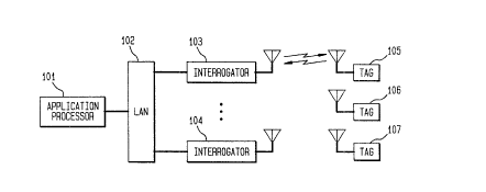
With .efe,~ce to FIG. 1, there is shown an overall block ~ g~m of
5 an illu~ e RFID system useful for describing the ~p~ ;nn of the lJL~lt.
invention. An Application Processor 101 co~ .ic~t~g over Local Area ~e:w~
(LAN) 102 to a plurality of Intel~ogators 103-104. The Inte~Togators m~y then each
co~.. - ~.ic~te with one or more of the Tags 105-107. For ~. ~k tho I~ ogatv~
103 l~e;~r~s an infonn~tion si~;nal, typically from an Arplic~tion Ploce,~or 101.
20 The Interrogator 103 takes this i.~r~J.. ~I;on signal and Processor 200 (FIG. 2)
~lo~.l~ fo~tc a downlink message (~.lfo- ~~ ;o~- Signal 20va) to ~e sellt to the Tag.
The infionn~tion signal (200a) i~ ~lion such as ;llrvllll~l;on s~ ,g which Tag
is to respond (each Tag may have fixed or pro~ .nP~ id~ ;on nurnber),
instructions for thc Tag's processor to c~ ~ or other i.~f~ ;on to ~: used and/or
25 stored by the Tag's pl~ocessor. ~With joint l~ f .ence to FIGS. 1 and 2, Radio Signal
Source 20~ ge - ~ 5 a radio signal, the Modulator 202 I~O~ ~S the: Infol~Lion
Signal 200a onto thc radio signal, and the T-~ -c ~ 203 sends this m~~ t~l
signal via Antenna 204, ill~LL~ ely using ~mrlit~ m~~ tion to a Tag.
,A.~ ~r modl tion iS a corrlmon choice since the Tag can dP n~hll~te such a
30 signal with a single, ;~- ~L ~;ve nonlinP~r device (such as a diode).
In the Tag 105 (see FIG. 3), the Antenna 301 (L~ Lly a loop or
patch ~ ,e.,;~,s the modlll~t~ signal. This signal is d- o~ tA~ di~,lly to
b~eb~ using the D~t~tor/Mo~ tor 302, which, ill~ ly, could be a single
Sch~,l~y diode. The diode should be ~ tely biased with a current level so that
35 the impedance of the diode m~chPs the i~ e~ce of the AnteD~a 301 such that
Iosses of the radio signal are n~in;...;,~ The result of the diode detector is
esse~ ly a demodulation of the i.~CO...il~ signal directly to bA~e~ The
CA 02219266 1997-10-23
.
Tl~fv....,~ n Signal 200a is then arnplified, by Amplifier 303, and ~..chlo~i~Lion
N:~O~ .~ in Clock and Frame Recovery Circuit 304. The Clock Reca~very Circuit
304 caD bc e~lh~n~ed by having the Interrogator send the arnplitude mofl~ terl signal
using M~ hP,k~ ~n~o-3ing If large amounts of data are being LL~sr~ ed in ~ames,
5 ~ame synchlo~ ion may be implen ~nt~l, for example, by ~et,ecting a
predet~rmin~li bit pattern that in~,icates the start of a i~arne. The bit paltern may be
~letected by clock recovery circuit (304) or processor (305). Bit pattem detection is
well known in the art. The reSulting infoTTn~on is sent to a Fioccssc,r 30S. TheProcessor 305 is typically an in~nsive 4- or 8-bit rnicl~opr~cessO, and its associated
o memory; the Clock Reco~ Circuit 304 can be impl~ ed in an.ASIC (Applied
Specifie Tn~e~ fl Circuit) which works together with Pi~essor 305. This Processor
305 can also serve as the driver for an optional Display Unit 309 should this Tag
require a display. The Processor 305 g~ 5 an ~fo~ ;on Signal 306 based on
the particular program being ç~cl~te~l by p.~essor 305. Signal 306 i~ e~e.,Llually
15 co~ ;ç~t~d from the Tag 105 back to the Interrogator (e.g., 'l03). This
Information Signal 306 is sent to a Modulator Control Circuit 307, w~ich uses the
Illfolll,Alion Signal 306 to modulate a Sl~bi~ frequency g~,-aled by the
s~ F1~ 1enC~ Source 308. The FI~u~nc~ Source 308 could be a crystal
osc~ t~r sepaLale fiom the FlLocessor 305, or it could be a L~.IU.~IL~;~r source derived
20 i~om signals present inside the P~Loce~ 305 - such as a divisor of the ~ILiLUL~L,~ clock
L~lu~cy of the Processor. The Mo~ tcd Subcarrier Signal 311 is used by
Detector/Modulator 302 to modulate the modulated signal received f~om Tag 105 t
produce a mc~ ted b~ t~ ~ (e.g., reflecte~) sig~l. This is ~co,~ lished by
xwil~,hi~g on and offthc Sch~,UI~ diode using the Mod7ll~t,ed S~ - Signal 311,
25 thereby cl~nging thc reflr~ of Antenna 301. A Battery 310 or other power
supply prov,id~ power to the CL1''CUih~ of Tag 105. Power may also be c~,cei~d, for
, by using iLL~lu~ , coup!Ling on micL~ w~V~5.
Modul~on
Therc are a variety of tec}~iques for using MBS to send i~fo...-~l;on
30 from thc Tag to the ~Lt~.logalor. In some MBS technologies, the Mo~ tor Control
Circuit 307 of the Tag gc ~ s an amplitude modulated signal m~llll~ted at an
~nform~hon Signal 306 L~.luen~i~ f2 ~ If the Radio Signal Source 201 g~ ,5 a CW
L. ~lu~,nc~ fc~ then the Interroga~.or receives signals at fc whose band~4id~h is 2f2
and filters signals outside of this bandwidth range. This app-oacll could ~le termed the
35 "MBS at b~ceb ~ ~1" a~p~vach
Another al)p~ach would be for the Tag to ge.~ h a subcarrier
fi~quencyf,l, gf ~ ~te~ by Frequency Source 308, as shown in FIG. 3. The
CA 02219266 1997-10-23
;,.f.~ l;on could be conveyed using AM, FSK or Phase Shift Keying (PSK) by
meui~ ting the a~ c~ ~r with a frequency of f, with the Tn ro~ on Signal having
a ~ equency f2 306. The ~nterrogator receives signal5 at fc whose bandwidthis 2f2 but at a frequency f, ~way from fc. This method is terme-i "MBS of a
5 subcamer".
In a Binary PSK l'BPSK) system the phase of the ~ul,c~l;er transitions
nomin~lly bc~ 0 and 180 degrees. We ~i~close here specific techni,ques to apply
Quadrature PSK (QPSK) to MBS a~ s. Based upon this ~lieclosll e, general levels
of phase modulation are possible (such as MPSK), or other complex modulation
lo 5çh~meS such as DiLt~,.e,lLially-encoded BPSK (DBPSK) or Di~.~ ially-encoded
QPSK (DQPSK).
When the Tag detects the ~l~sellce of the ~nte~rogator downlink signal
it responds by tr~n~mitting its RFID data In one embo~lim~nt, the Ta~ .e~lially
encodes the uplink data and uses the di~.clllially ~ ro~e~ data to QI'SK m~~ tç
5 the ~ .;~. The QPSK mcYllll~t~ a ~-lbc~ 311 m~~ t~q the reflectet CW
signal, which has a ~ u~llL~;r ~fc by chA~gi-~g the refl~~ r4 of A'~tf ~ 301 using
signal 311. FIG. 4 shows the b~ceb~ neo~ling ~lgo.;lh... for DQP'3K The data
bits, at rate f2 (for example, 100k bit/sec, are taken two at a time, Gray ~nrod~ and
then the Gray encoded bits Gl aLnd GQ are added to the previous phase of the QPSK
20 mo~ ted signal; the result is the present phasLe of the bA~bAl~ DQPSK signal.Gray encoder 410 does a simple co~e. ~ion in accol~,cc with the followi~g: IQ = 00
~ GlGQ = 00; IQ = 01 ~ GlGQ = 01; IQ = 10 ~ GlGQ = 11; IQ = 11 ~ GlGQ = 10.
The outputs, G,GQ of Gray enro~ 410 are provided to phase adder 420. Phase
adder 420 simply does a module 2 addition of GIGQ and the present value of Gl'GQ'
25 to produce the new vaLlue Of Gl' GQ' . For c.~ le if GIGQ = 1 1 and the present value
of Gl'GQ'-= 01 the new value oi. GIGQ = 00. The il~fo....~l;on sigr~al (306) is used to
m~~ te the ~ .;~ which has a L~ f5(for ~Y~rnrle 250 k~); the
Mo~ t~l~ S~L~bC~ r Signal 311 is used to control thc refle~L~L~ of the Detector
Modulator 302 thereby sçnrling a CW signal (having L~U-~IL~;~r fc) that has been30 modlll~ted by the DQPSK mod.ulated ~ r back to the Inte~rogal:or. For QPSK
systems the Interrogator receives signal~ at fc whose bandwidth isf2 but at a
frequency f5 away firom fc-
There are at lea,t two ways in which to nl~hll~t.e the~:ivlx~-~;er 311.
The first ml-thf--l derives the subcarrier fro~m the rnic~p~ces~or crystsll circuit (312)
35 and is gene.~ed intern~lly by the microprocessor 305. Here the DIQPSK data isstored as a phase "word" inside the micr~p.ocess~r ~e,--~.~. During uplink
~cmicsion the word ~e~,es- ~~t;,~g the current data bit is written to an ~~xt~m~l Port to
.
CA 02219266 1997-10-23
pr~ducc 306 which controls the I)~CL~ e~ g m~~ t~r 307. The wol.di3 shif'~ed
out the Port at twicc the s~ rier frequency rate thereby prodncing the desired
s~1bcs .;~ L~.lu~n~ fJ. For ex.arnple, to get a square wave of frequency f5, an
altf ~ ;..g l.0 pattern is written to the port at a rate of 2f, . The number of cycles in
5 which the word is shif'ted out of the Port produces the desired channel symbol rate of
the DQPSK modulated uplink sigllal. (This is half the C~ ~nn~l symbol rz~te of BPSK
and resllltin~ in the cl~nnpl bandwidth f2 described above.)
The second mf~th~dl for ge~e.~i.lg the mo~ ted uplinlc is to generate
the subczlrrier fi..luc~ e~rn:~l to the mi~;lu~cessol 305. ~n one embo-liment,
o FIG. 5, a ~to-l ml~1tipl~Yor 503 is used as the QPSK m~~ tor contra~l 307. The
multiplexor selects the ph~ie of the SI~ ;L- 3 l l by the current value: of G~' and
GQ', written to the select lines of the m~ ip1.elt~r from the processor port as signal
306. The subcarrier sigclal can be ge ~ from thc microprocessar's eYt~Tl:~l
crystal or clock circuit 312 by co.-.-r~ g a buffcr circuit 501 and a cligital clock
lS divider circuit S02 (if llFCe j~ ~r) to the mi-,~uploce~l s clock circuit 31:2. The two
O-flip-flops c~...l..;~;..~ clock divider circuit 502 prc~duce the 4 ph ce ihifts of the
subc~ r signal 504 and mllltipleYnr 503 selects one of thc 4 pha~es ~lased ûn the
signals Gl' and GQ' which are p~ te;l at ~ulLipleAol 503's select inputs. FIG. 6s the relationship ~l~ the output of buffer 501 and the OUtpUl s of the two
20 O-flip-flops~ The ~ . . ;c~ signaLlL 504 is phase mod~ t~ by the mulLtiplexor circuit
503; thereby producing the secondL ~o....;~l;on signalL.
The mPth~ des,cribed above for either int~n~lly o;r çxt~sllly
geLc.d~ g the mo~ t-P~l a~llx~.;c~ signal 311 are PYtPn~lible to M-ary Phase Shift
KeyedL mo~llll~ti~)n For ~ Il '~ DMPSK ~ es that the dLata bits be Gray encod~
25 M bits at a time and the digitalL clock divider wilL need dddLitiona]L stages t~ prodLuce
the M phase shifts of thc avl)c~ sig~ ; arl M-t~l mulliplc.~or is used as the
modulator colltroller 307.
R~~t~
E2l.~....;.~g to FIG. 2, the Interrogator 103 r~e;~._s the reflected and
30 modlll~t~ signal with thc Receive ~nterln~ 206, ~mrlifi~ the signal with a Low
Noise ~mrlifier 207, and rlPmr~ tes the signal using homodyne ~letec~ion in a
Mixer 208 down to the r--~ -r~ c Fle.~ "~ ) of the single ~ulxaLLL;c~ fs . (J~l
some Interrogator decign~, a single T.~..~...;~l., 204 and Receive 206 Antenna is used.
In this event, an cle_l~ùnic m~tho-l of sepA- ~ g thc l...,c..,;ll~ signal ~om that
35 leCeived by the receiver chain is n~ede~l this could be acco~ lished by a~ device such
as a Circulator.) Using the salm~e Radio Sigrlal Source 201 als used in the l.~ ---it
cha~in~ meauls the demodulation to IF is done using Homodyne detection; this hals
.
~ CA 02219266 1997-10-23
a~lv;~ g~ ~ in that it greatly reduces phase noise in thc l~;C;~ circuit~'. The Mixer
208 th~ send~ a DÇmoi~ t~ Signal 209 -- if using a Ql.z.1.,.~ Mixer, it sends
both I (in phase) and Q (q~ r~1llre) signals ~ into Filter/~mplifier 210 to filter the
Demod~ t~ Signal 209. The resl~lting filtered signal ~ then typically an
5 I~ lion Signal 211 carried on an IF sllhcz..;c. is then demodul.lted from the
subcarrier in the S~ rrier Demodulator 212, which then sends the~ lnformation
Signal 213 to F~ocessor 200 to ~ieterlT ine the content of the ~ ~ge. The I and Q
~hA~ el~ of Signal 20~ can be: combined in the Filter/~mrlifiP~ 2L0, or in the
S~ nPr Demodulator 212, or they could be combined in the Pnxes~l 200.
The are several cbloices for impl~ P~ g thc data lceu~ 212 part of
the ~ t;~ r hal~lW~; co~ ional analog I/Q ~Pm~ ;On of the a~ItIC5" 1 ;l signal
u~sing, e.g., a Costas Loop, Digital Signal P10CP~ 3 (DSP) of the ;~ ,1ed
s~ rrie~, or imrll~ . c~.l;,~p a L~Ce;~e~. in digital logic. Since ....I~ the system
cost i~ one obje~Li~,~, one emb~imPrlt of thia invention ha~ been i~ in
15 digital logic.
The data l~cove.~/ circuit 212 is ;...p~ ,. .,t~A in Gate A~ray circuit,
FIG. 6. It has two functions:
1) ~Pm-~dlll~tion of the diLr.,ne~llially P ~ oded phase shift l~eyed data
(data recovery circuit), and
2) deriving the received bit clock for the dP~nod~ t~l data stream
(clock l~,CO~ circuit).
The input to the data recovery ciircuit 212 is the hard limited ~ ;c~ 601, which is
mo~ t~Pd by dirr~,.e~lial QPSK~ The subcarrier 601 is r~l-d at L~ rate F,
(for example, 4 M~) 601a, and is input to a N+2 stage shiiflt le~ter 602 (in this
example, N=80), the Nd' stage providing a one symbol delay 603 (th~: shiflt register
602 is also clocked at the s~mpl ing rate F, ). The N+2 stage is ~ ~ rd to alv~ce the
re m~llls~t~ a~ ;Pr sigrlal by 45~ 603a and the N-2 stage ~jO3b i~ at 15~
relative to thc .~ 601. ~he s~mrleA allbc5 . - ~ 601 ia c ~ ;5~l1y multiplied
with ea~:h of the delayed a~lbc~ ers 603a and 603b (using e.~ R gates) 604
3Q and the regults are filtered by ~ccllm~ tor circuits 605, which are the digital
equivalent to the classic inte~rate and dump (Matched Filter~ lece;~,.,r, which
i~te~dtes over one symbol pe~iod (in the e~5~ )1e, one symbol period is N periods of
shift le~3;a~,1 602's clock, where N=80 and Fs = 4M~). The output of the
to~.~ are passed to symbol decision CO...~ O.~ 606 and the rç~llting
35 decision symbols are the I and Q i~ on symbols bits, which a~re multiplexed
(i.~t~le~ed) to produce the dem~l~l~ted data st~eam 607. With regard to symbol
decision colllpal~l ,ls 606, if the output of the ~c~~ml~l~tor is greater than or equal to
CA 02219266 1997-10-23
r
N12 (in thi~ N/~2 = 40) C15~ aLOl 606 outputs a 1, aDLd if tbLe ol~tput of the
r is less thanL N/2, co~l~a.ato- 606 outputs a 0.
Aflter inform~tion bit demodlllation, the data clock is be gen~
The demodulator impl~ments a ~l~imtlTn A P'o~ ; (MAP) bit timing c ircuit. TbLe
5 demodulated da~a is sent to a bank of correlators 608, each of which is testing a
different clock phase. The correl~Ltors l~leA~ulc the ~lignmPnt of the inp-[t daLta witbL
their clock over a B data bit window. The B bit window is 8 data bits 'iong iDLt_iS
ç~mple; ho~ ., larger values af B are less s~ , to long s~i~Lgs of l's or O's,
but require- more hardware (or sof'tware/time) to imrleTn~nt Each correlator is made
0 from an ;..t~ e-aDId-dump filter, a weighting function t~t give igher weight to
igh sig~ to-noise data, and an aCc~m~ tor (that acc~mnl~t.~ over a p~:riod of B).
A weight n~ function is not required, but it is possible to give higher weight to higher
corTelator outyuts and lower weights to low co.lelalo~ outputs. Far c~ylc,
coll~lalor outputs a~pl~oarhing +1 or -1 are m~lltirliPd by a factor of 10, and co~l~r
Is outputs ayy.o~cl~;--g 0 are given a value equal to the squarc root of the acbual outpu~
Af ter B bits have been ~ n~ the col.~lator with the highest ~cl~rn~llzltor value i~
found alld it3 A~SO'';AhA clock ph;~,e 609 is used to sampb the next B ~its of data.
The ~ tor is dlen reset, and the next B bits arc --~ ..;..Pd Thc hlly~ uLthing
here is that thex is no memory from one set of bits to the next, every B bits the clock
20 estimAt on circuit ~ ,.k a new e~ l* of the best clock phase th~1t dloes not
depend on previous e~ is lets us acquire a bit clock quickly - providing a
bit clock even for modest SNR. Prior art l--A~ !C that a Phasc Locked I,oop (either
analog or digital) be used in clock ~c~ r. However, Phase Locked Loops have a
111;~-;---1---- "lock-up" tiIne that is a fimchon of the loop filter. This lock-~lp time also
25 ll~ea~3 as system noise I~ClCa~'~ and are unreliable for modest SNR
- Th~ are s.few other f;mrtion~ that may be i~co~at~ in the Gate
Array chip; for examplc, the largest co~l~,lator value is ~ eO see if it is highe.r
than a fi.~ced threshold. If it is, a signal is ~c~,~t~d in~ c~ g that thc bit clock is
valid 61~ The r. .. g scheme uses a Barker code to intlic~ the st~rt of the payload
30 data. The p~cse~cc of the Bar~;er word is df~t~ and ~.. ~e~ a signal that
inllic~t~s that the next bit is p~rt of the payload 611.
The m~thntls described above ~nn.l..l;.l;.~ the . ~)le.~ x~,~5..,;.,
signal.601 are e~ n~lible to M-ary Phase Shift Keyed mq~ ffon For eY~ml~lc,
DMPSK ~.luLLes a.l~lition~l shiflc register delay stages to p~luce the M phase shif~s
35 of the sampled m~ t~l xubc~.icr signal and the ~d~liffon~l XOR, ~cumlll~tQr and
~leci.~ion circuits to decode the M paral1el bit paths.
CA 02219266 1997-10-23
,
The methods c an also be ~xt~on.led to more sophi ;ticated phase
m~~ tion s-~P~ 3 such as MSK (~i~ Shift Keyed), GMSK ((~ n
Shift Keyed), etc. For MSK, pre-co~uled phase tran~ili(m~ could be
stored in the processor's memory. Also, for example, through computation in the
s processor, the Tag can g~ elate a smooth transition from one p~ase to another, and
thereby produce an al~)fo~iately filtered phase modulation to produce a GMSK-
modulated subcanrier. Other phase modulation sch~ s are also possib] e.
Using the above tecbmiques as an example, an in~ le;~e~ short-
range, bi directional cligital racLio commnnic~tion~ channel is imrl~ nt~l These0 techniques are inexpensive as tb~e Tag co~ ents consist of (for eY~ le) a Schottky
diode, an amplifier to boost the signal strength, bit and frame synchro~ l ion circuits,
an inc:~ive 4 or 8 bit microprocessor, subcarrier generation circuits,, and a battery.
Most of these items are a~ready m~nllf~tllred in large q~l~nt;~ for other
application~, and thus are not overly e~nsi~le. The circuits mentioncd above forIS subcarrier generation may also be lmp~ t~si in logic surrounding the
microprocessor core; tb~us, excl pt for a relatively small a~ount of cl~ip real estate,
these fim~tion~ come almost"for free."
What has been described is merely ill~ " of thc application of the
p~ln~i~les of the present invention. Other ~n~nge n~nt~ and methods can be
20 i..\pl~ ted by those skilled in the art without de~ling from the spirit and scope of
the present inven~on.