Note: Descriptions are shown in the official language in which they were submitted.
CA 02219349 1997-10-23
W O 97/06453 PCT/CA96/00463
-- 1 --
MOTION ~ ~~ ON ~ ~TNq DE~VIC~ A~DD I_~
F:~ELD OF THE lN V ~:N-l'lON
Thi~ invention relate~ to a motion detection
and imaging device and method, ~uitable for security
purposes for the surveillance of a protected area.
RA~ROUn~D OF THE lNV~:NllON
Variou~ t~rpes of security systems for
monitoring a protect:ed area and ~-k; ng a recording of an
image of a per~on entering the area, are known.
Normally t:hese sy~tems are expen~ive and
comprise various int:er-connected component~ in different
location~ and require on-~ite supervisory personnel. It
is an object of the present invention to provide a self-
cont~;n~ UDLit which can easily be in~talled in an area
to be monitored withi no human intervention being requLired
after in~tallation until such time a~ the recorded images
are required.
SUMMARY OF THE lN V ~:N l lON
According to the invention there is provided a
motion detection and imaging device comprising a housing
cont~;~;ng a CCD for providing digital image data, a len~
for focusing an image to be observed on the CCD and a
solid state non-volatile memory for ~toring ~aid digital
image data.
The lens may compri~e a wide angle len~
assembly. The len~ may include an electronic shutter.
CA 02219349 1997-10-23
W O 97/06453 PCT/CA96/00463
-- 2
The device may further comprise means for
controlling opening of the shutter at predet~m; ne~ time
intervals for intermittently focussing an image on the
CCD.
The device may further comprise a motion
detector for triggering the storage of the digital data
in the memory.
The device may also comprise means for
compressing the digital data prior to storage in the
memory and means for decompressing the data after
retrieval from the memory.
The device may further comprise an electronic
clock and calendar for t;~;ng and dating the digital
data.
The device may also include a source of
illumination.
Also according to the invention there is
provided a motion detection and imaging method comprising
the steps of focusing an image of an area being monitored
2 5 on a CCD by mean~ of a lens to provide digital image data
and storing the data in a solid state non-volatile
memory.
The image of the area being monitored may be
focused on the CCD intermittently at predete~m;ne~ time
intervals to provide digital image data of a series of
separate still pictures which is stored in the memory.
Further objects and advantages of the invention
3 5 will become apparent from the description of a preferred
emboA; ~nt of the invention below.
CA 02219349 1997-10-23
W O 97/064~3 PCT/CA96/00463
-- 3
BRIEF DESCRIPTION OF THE DRAWINGS
The single drawing i8 a schematical
representation of a motion detection and imaging device
according to the in~ention.
DET~TT.~n DESCRIPTION OF PREFERRED E~30DIMENT
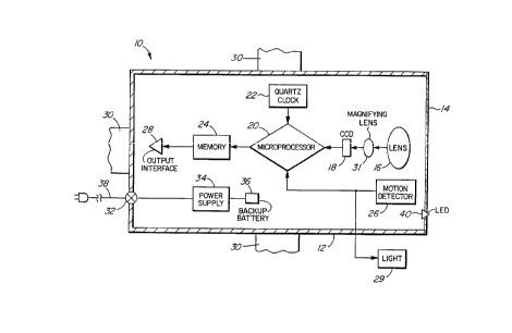
In the dralwing, reference numeral 10 generally
indicates a motion detection and imaging de~ice. The
device 10 comprises a tamper resistant housing 12
pro~ided with a transparent front 14. The housing 12
aontains a wide angle lens ass~-~bly 16, a charge coupled
imaging device (CCD~ 18, a microprocessor 20, a ~uartz
crystal controlled c:lock and calendar 22, a - ~ bank
24 comprising one or more solid state non-volatile high
density memory chip~~, a microwa~e or ultrasound motion
detector 26, an output interface 28 and a light 29. Due
to the disparity bet:ween the size of a wide angle lens
image and the dimini.ti~e size of a CCD, a magnifying lens
31 is placed in front of the CCD 18 80 that the entire
image from the lens ass~hly 16 will be recorded.
The device 10 further includes a key-operated
on/off switch 32, an AC to DC converter, voltage
regulator and battery charger 34 and a backup battery 36.
A secured AC power ~upply connection 38 is provided for
connecting the converter/regulator/battery charger 34 to
an external power supply.
In the present example, the lens assembly 16
has a fixed focal length and incorporates an electronic
shutter controlled ~y the microprocessor 20. The lens
ass~hly 16 is mounted in front of the magnifying lens 31
for focussing an image of a protected area on the CCD 18.
The CCD 18 produces a digitized image, the data of which
CA 02219349 1997-10-23
W O 97/06453 PCT/CA96/00463
-- 4
is fed to the microprocessor 20. The digital image data
is compressed by the microprocessor 20, using a suitable
compression/decompression algorithm, e.g. according to
the JPEG (Joint Photographic Experts Group) st~n~d.
5 The compressed data is then stored in the memory bank 24.
The size of the memory bank 24 is determined by the
number of images which are required to be stored, the
resolution and grayscale of the images, as well as the
compression/decompression algorithm being employed.
The microprocessor 20 is plOy -~ to store
the compressed images sequentially on a first in first
out basis 80 that the ~-~; number of the latest
recorded images, dependent on memory size, is available
15 for retrieval.
The microprocessor 20 is ~oy - -~ to store
the images at intervals, not continuously. Therefore,
still images of the area being monitored will be stored
20 at predete~m;ne~ intervals, which intervals may be
selected to be relatively short, i.e. to provide a ~uick
sequence of images, or the intervals may be longer, as
desired. In order to achieve this, the microprocessor 20
will control the electronic shutter to open at the
25 predet~m;ne~ intervals.
The storage of an image in the memory 24 is
triggered by v -nt in the protected area, which is
detected by the motion detector 26. The motion detector
30 26 also triggers the light 29, dependent on prevailing
lighting conditions. t
The electronic clock and calendar 22 operate to
provide a time and date for the stored images.
CA 02219349 1997-10-23
WO 97/06453 PCT/CA96/00463 -- 5
The devic:e 10 i~ operated by a voltage
regulated DC power supply provided by the converter 34
from an external AC power source. The battery 36 serves
as a back up ~houlcl the AC power supply be interrupted.
The device 10 incorporates circuits with ~elf-
diagnostic functions and external LED indicators 40 are
provided to indicate various failure modes, as desired.
In use, the housing 12 is installed in a
location which is cLifficult to access but with a good
view of the protected area to be monitored. Brackets 30
or other suitable means are provided on the housing 12
for mounting the housing 12 in pogition.
The motic,n detector 26 will detect .~v~ -nt in
the protected area being monitored. This triggers the
operation of the de!vice 10 to receive, compress and store
the images of the area in the memory 24. In the event of
a security breach, the device 10 can be detA~he~ and
connected to a PC clr laptop with the appropriate software
for viewing the latest series of recorded images. The
stored images are available for retrieval and
~e~ rression for analysis or -nh~ncement, using
interpolation techniclues. If desired, a hard copy output
can be provided.
The device 10 is provided as an integral
st-~n~lone unit with all its c~ _ -nts housed in the
housing 12. It employs the low density imaging
capability of a charge coupled device through a wide
angle lens assembly with the high data storage density of
a non-volatile memory chip(s).
CA 02219349 1997-10-23
Wo97/06453 PCT/CA96/00463
-- 6
Instead of using a lens assembly with a fixed
focal length, provision may be made for auto-focussing of
the lens assembly to provide for a better picture.
Further ref;n~nts may also be provided, such as for
example, automatic control of the lens aperture and
shutter speed dependent on the lighting conditions.
While only preferred ~mbodiments of the
invention have been described herein in detail, the
invention is not limited thereby and modifications can be
made within the scope of the attArhe~ claims.
-