Note: Descriptions are shown in the official language in which they were submitted.
CA 02219761 1997-10-28
WO 96/35155 PCT/US96/05749
PRINTED CIRCUIT BOARD WITH SELECTABLE ROUTING
CONFIGURATION
FIELD OF THE INVENTION
The present invention pertains to the field of printed circuit
boards. More particularly, the present invention relates to
reconfiguring the electrical routing configuration of a printed circuit
board after completion of the manufacturing process.
BACKGROUND OF THE INVENTION
Printed circuit boards are commonly used in the computer
industry and in numerous other areas of technology to implement
electronic circuitry. A printed circuit board typically consists of one or
more substrate layers made of a dielectric material, on which
electronic components are mounted. One or more layers of
conductive material, such as copper, are mounted on and between the
substrate layers to form the wiring, or "traces", that interconnect the
electronic components. The traces may be formed by fixing a solid
metal plane onto the surface of a substrate layer and then etching the
metal plane according to a pattern. The traces are typically covered by
an insulative protective coating, with the exception of certain portions
which are left exposed for the purpose of providing bonding contacts.
Because there are so many potential uses for printed circuit
boards, it has become desirable to provide the capability to mass
produce a printed circuit board which has a single generic routing
configuration, but which later can be tailored to have one of multiple
specific configurations. Various solutions have been developed to
accomplish this goal. For example, a "zero-ohm" resistor, or jumper,
can be used to electrically connect two traces on a printed circuit board
to modify the routing configuration. This solution is
disadvantageous, however, because it is not cost effective to purchase
and maintain an inventory of separate components for this purpose.
One way to overcome this disadvantage is to use solder instead of a
~ zero-ohm resistor to connect two traces and thereby modify the
routing configuration. There are many situations, however, in which
it may be desirable to adjust the routing configuration of a printed
CA 02219761 1997-10-28
WO 96/35155 PCT/US96/05749
-2-
circuit board during the post-manufacturing test phase. Yet both of ,
the above-mentioned solutions may be impractical to implement once
the manufacturing process has been completed.
One situation in which the post-manufacture configuration of a
printed circuit board may be desirable is the production of personal
computer (PC) motherboards. A PC motherboard, which contains the
central processing unit (CPU) of the computer, may also contain a
dedicated power supply for the CPU. The CPU requires a regulated
power supply which will provide a very precise voltage; often a
tolerance of less than 1 % is required. However, power supply voltages
tend to vary depending upon load, temperature, noise, and
manufacturing tolerances. Consequently, the "set point" of the
regulated power supply must be carefully adjusted. The "set point" is
the regulated output voltage at a steady load and temperature.
Typically, the output voltage of a power supply is measured during
testing. Power is then removed, and the set point is adjusted
according to the measured output voltage.
One way to permit the adjustment of the set point is to provide
a feedback circuit comprising a resistor divider network, as illustrated
in Figure 1. Figure 1 is a block diagram of a regulated power supply 1
having a feedback circuit 20 comprising a simple resistor divider
network which is well-known in the prior art. The resistor divider
network consists of a resistor RX having a fixed value and a variable
resistor RY. The value of resistor RY is varied manually to adjust the
output VgB of the divider network to adjust the set point of the power
supply. This solution is disadvantageous, however, because the
resistor RY requires mechanical adjustment, and because its value
may tend to drift once the motherboard is installed and operating in a
PC.
Therefore, it is desirable to provide for the mass production of a
printed circuit board having a single routing configuration which can
be easily reconfigured to have one of multiple different routing
configurations. It is also desirable to make reconfiguration practical
and convenient even if performed after the manufacturing process
CA 02219761 2001-02-21
-3-
has been completed. It is further desirable to provide a means for
configuring the trace routing on a printed circuit board such that a
separate inventory of parts need not be maintained for that purpose. In
addition, it is desirable to provide a regulated power supply which has
a set point that is adjustable during post-manufacture testing and which
incorporates the aforementioned features.
SUMMARY OF THE INVENTION
A printed circuit board having a selectable circuit routing
configuration is described. The printed circuit board comprises a
substrate, a plurality of electrical traces mounted to the substrate for
interconnecting electrical components, and at least one fusible
connector mounted to the substrate. Each of the fusible connectors
comprises a fuse line formed from a conductive layer of the printed
circuit board and forms a fusible connection between at least two of the
electrical traces. The circuit routing configuration is selectable by
application of a predetermined current through at least one of the
fusible connectors to break the fusible connection formed by the
fusible connector.
The fusible signal connector comprises a first contact pad
located at an end of a first signal trace on a printed circuit board, a
second contact pad located at an end of a second signal trace on the
printed circuit board, and a fuse line. The fuse line is formed from the
conductive layer of the printed circuit board and is fusibly coupled
between the first contact pad and the second contact pad. The
CA 02219761 2001-02-21
-3 a-
predetermined current driven through the fuse line causes the fuse line
to fuse open.
Accordingly, in one aspect, the present invention relates to a
method of providing a circuit board having a selectable circuit routing
configuration, the method comprising the steps o~ forming a
conductive layer on a substrate; forming a plurality of electrical traces
from the conductive layer; and forming a fusible connection from the
conductive layer between at least two of the electrical traces
simultaneously with said step of forming the plurality of electrical
traces, such that a circuit routing configuration of the circuit board is
configurable by application of a fusing current through the fusible
connection to cause the fusible connection to fuse open.
In a further aspect, the present invention relates to a method of
producing a circuit board, the circuit board having a circuit routing
configuration, the method comprising the steps o~ forming a plurality
of electrical traces and a fusible connection between the electrical
traces from a conductive layer of the circuit board; and verifying the
routing configuration of the circuit board as part of a test phase; and
configuring the circuit routing configuration of the circuit board as part
of the test phase by applying a current through the fusible connection
to fuse open the fusible connection.
In a still further aspect, the present invention relates to a method
of producing a circuit board, the circuit board having a circuit routing
configuration, the method comprising the steps of: forming a
conductive layer on a substrate; forming a plurality of electrical traces
from the conductive layer; and forming a fusible connection from the
CA 02219761 2001-02-21
-3 b-
conductive layer between at least two of the electrical traces; testing
the routing configuration of the circuit board during a test phase; and
configuring the circuit routing configuration of the circuit board during
the test phase by applying a current through the fusible connection to
fuse open the fusible connection.
In a further aspect, the present invention relates to a method of
providing a circuit board having a selectable circuit routing
configuration, the method comprising the steps of: forming a
conductive layer on a substrate; forming a plurality of electrical traces
from the conductive layer; and forming a fusible connection from the
conductive layer between at least two of the electrical traces;
connecting the circuit board to test equipment; and using the test
equipment to apply a fusing current through the fusible connection to
cause the fusible connection to fuse open; and using the test equipment
to verify the routing configuration of the circuit board without
removing the circuit board from the test equipment.
Other features of the present invention will be apparent from the
accompanying drawings and from the detailed description which
follows below.
CA 02219761 1997-10-28
WO 96/35155 PCT/US96l05749
-4-
ERIEF DESCRIPTION OF THE DRAWINGS .
The present invention is illustrated by way of example and not
limitation in the figures of the accompanying drawings, in which like ,
references indicate similar elements and in which:
Figure 1 is a block diagram of a regulated power supply having a
resistor divider network according to the prior art.
Figure 2 is a block diagram of a regulated power supply having a
resistor divider network with fusible connectors.
Figure 3 illustrates a fusible connector according to one
embodiment of the present invention.
Figure 4 illustrates a fusible connector implemented on
multiple layers of a printed circuit board.
DETAINED DESCRIPTION
A printed circuit board having a selectable circuit routing
configuration is described. In the following description, for purposes
of explanation, numerous specific details are set forth in order to
provide a thorough understanding of the present invention. It will be
evident, however, to one skilled in the art that the present invention
may be practiced without these specific details. In other instances,
well-known structures and devices are shown in block diagram form
in order to avoid unnecessarily obscuring the present invention.
Figure 2 shows a regulated power supply 2. The regulated
power supply 2 consists of a regulator 10 which receives an input
voltage V~ and which generates an output voltage VOUT. The
output voltage is input to a feedback circuit consisting of a resistor
divider network 25. The resistor divider network 25 outputs a
feedback voltage VFg to a comparator 30. The comparator receives the
feedback voltage VFB and a reference voltage VREF and outputs to the
CA 02219761 1997-10-28
W O 96/35155 PCT/US96/05749
-5-
regulator 10 an error voltage ERROR which is proportional to the
difference between the feedback voltage VFg and the reference voltage
VREF. The functions performed by the combination of the
comparator 30 and the reference voltage VREF may be implemented
using well-known integrated circuits, such as the TL1431 or the TL431.
The resistor divider network 25 consists of six resistors Rl
through R6. Set Point resistor Rl is coupled between the output
VOUT of the regulator 10 and the VFB input of the comparator 30. Set
Point resistor R2 is coupled between the VFB input of the comparator
30 and ground. Resistors R3 and R5 are coupled in parallel with Set
Point resistor R1, while resistors R4 and R6 are coupled in parallel
with Set Point resistor R2. Each of resistors R3 through R6 is coupled
to the VFB input of the comparator 30 through a separate one of four
fusible resistors 40.
The regulated power supply 2 has a set point which represents
the output voltage VOUT at a constant load and temperature. The set
point may be adjusted by adjusting the feedback voltage VFB input to
the comparator 30 for a given output voltage VpUT. In other words,
the set point may be adjusted by changing the transfer function
VFB/VOUT of the resistor divider network. This is accomplished by
breaking the current path through one or more of resistors R3
through R6. Consequently, the set point of the regulated power
supply 2 may be adjusted by selectively fusing open one or more of the
fusible connectors 40.
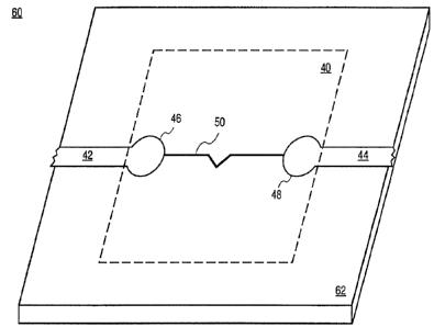
Referring now to Figure 3, a section 60 of a printed circuit board
is shown. The printed circuit board consists of a substrate 62 and
multiple copper traces, including traces 42 and 44. Traces 42 and 44 are
terminated in copper contact pads 46 and 48, respectively. Coupled
between contact pads 46 and 48 is a fuse line 50. A fusible connector 40
' comprises the contact pads 46 and 48 and the fuse line 50. In the
preferred embodiment, the contact pads 46 and 48, the fuse line 50, and
the traces 42 and 44 are all formed simultaneously from a single
copper layer by the same etching process. Although the traces on the
printed circuit board 60 are generally covered by a protective layer of
CA 02219761 1997-10-28
PCT/US 9 6 I 0 5 7 ~. 9
IPEAI(lS 2 ?' ,l UN 199
6
insulating material, the contact pads 46 and 48 are exposed to allow
electrical contact with a test probe or other similar instrument.
The fuse line 50 may be fused open by applying a predetermined
voltage between contact pads 46 and 48 to cause a fusing current to
flow through the fuse line 50. The width and shape of the fuse line 50
are calculated such that the fuse line 50 will fuse open at the lowest
possible fusing current and provide the cleanest break upon fusing,
subject to current manufacturing capabilities. A fuse line 50 having a
_ kinked shape as shown in Figure 3 may be suitable for this purpose.
In addition, the length of the fuse line 50 is as short as possible
according to current manufacturing capabilities. The contact pads 46
and 48 and fuse line 50 are sized and shaped in order to provide
negligible resistance.
The present invention may also be embodied on a multiple
layer printed circuit board, as shown in Figure 4. The fuse line 50 is
formed on one substrate layer 63 of the printed circuit board while the
traces 42 and 44 are formed on a different substrate layer 64.
Connection between the fuse line 50 and contact pads 46 and 48 is
made through vias 52 and 54.
Hence, the routing configuration of the printed circuit board 60
can be easily altered after the manufacturing process has been
completed (e.g., during the testing phase) by selectively fusing open
any of the fusible connectors 40. By applying a predetermined voltage
between contact pad 46 and contact pad 48 to cause a predetermined
current to pass through and to fuse open the fuse line 50.
Furthermore, if this process is performed during the testing phase, the
open/short condition of the fusible connector 40 can be easily tested,
since the printed circuit board is already connected to the test
equipment. Therefore, the printed circuit board 60 can be mass
produced to have a single routing configuration that can be easily
reconfigured into one of multiple different routing configurations. It
is not necessary to maintain a separate inventory of parts for the
purpose of performing such reconfiguration. Furthermore, the fusible
connector 40 can be implemented in a regulated power supply such
~NIE~DEJ SM~r~'
CA 02219761 1997-10-28
WO 96!35155 PCTYUS96I05749
_7_
that the set point of the power supply can be easily adjusted during
testing without the need for mechanical adjustment of a variable
resistor, and such that the set point has minimal variance during
operation.
Although the present invention has been described with
reference to specific exemplary embodiments, it will be evident that
various modifications and changes may be made to these
embodiments without departing from the broader spirit and scope of
the invention as set forth in the claims. Accordingly, the specification
and drawings are to be regarded in an illustrative rather than a
restrictive sense.