Note: Descriptions are shown in the official language in which they were submitted.
CA 02220031 1997-11-03
WO 96/36080 PCT/LTS96/05160
-1-
DOUBLE HETEROJUNCTION LIGHT EMITTING
DIODE WITH GALLIUM NITRIDE ACTIVE LAYER
Field of the Invention
The present invention relates to light
emitting diodes, and in particular, relates to light
emitting diodes formed in semiconductor materials with
-sufficiently wide band gaps to emit light in the blue
portion of the visible spectrum.
Backcrround of the Invention
A light emitting diode ("LED") is a photonic
semiconductor device. Photonic semiconductor devices
fall into three categories: devices that convert
electrical energy into optical radiation (LED's and
diode lasers), devices that detect optical signals
(photodetectors), and devices that convert optical
radiation into electrical energy (photovoltaic devices
or solar cells).
Although all three of these categories or
devices have useful applications, the LED may be the
most commonly recognized because of its application to
such a wide variety of products and applications such
as scientific equipment, medical equipment, and perhaps
most commonly, various consumer products in which LEDs
form the light source for various signals, indicators,
gauges, clocks, and many other-familiar items.
Semiconductor sources such as LEDs are
particularly desirable as light output devices in such
items because of their generally long lifetime, their
~ low power requirements, and their high reliability.
In spite of their widespread use, LEDs are to
some extent functionally limited, because the color
that an LED can produce is fundamentally limited by the
nature of semiconductor materials in which the LED is
formed. As well known to those of ordinary skill in
CA 02220031 1997-11-03
WO 96!36080 PCTILTS96I05160
-2-
this and related arts, the light produced by an LED is
referred to as "electroluminescence" and represents the
generation of light by an electric current passing
through a material under an applied electric field.
Any given material that produces electroluminescent
light tends to do so over a relatively narrow range of
wavelengths under given circumstances. -
Electroluminescence thus differs from thermal radiation
or incandescence which generally have much broader
spectral widths.
More fundamentally, an LED's luminescence is
produced by basic quantum mechanical transitions
between energy levels within the semiconductor
material. Because the bands within a material depend
both upon the material and its doping, the energy of
the transition, and thus the color of the radiation it
produces, is limited by the well known relationship
(E=hv) between the energy (E) of a transition and the
frequency (v')- of tine light it-produces (h-is Blank-'-s
constant). Blue light has a shorterwavelength (and
thus a higher frequency) than the other colors in the
visible spectrum, and thus must be produced from
transitions that are greater in energy than those
transitions which produce green, yellow, orange or red
light.
More specifically, the entire visible
spectrum runs from the violet at about 390 nanometers
to the red at about 770 nanometers. In turn, the blue
portion of the visible spectrum can be considered
(somewhat arbitrarily) to extend between the
wavelengths of about 425 and 480 nanometers. The
wavelengths of 425 and 480 nanometers in turn represent ,
energy transitions (also somewhat arbitrarily) of about
2.6 eV and about 2.9 eV. Accordingly, only materials ,
with a bandgap of at least about 2.6 eV can produce
blue light, even under the best of conditions.
CA 02220031 1997-11-03
WO 96/36080 PCT/US96I05160
-3-
As is further well recognized, blue is one of
the primary colors, and thus any devices which hope to
produce full color-displays usingLEDs need to
incorporate blue in some fashion. Absent efficient
blue LEDs, some other method such as filtering or
' shuttering must be used to produce a blue contribution
to a display that otherwise lacks a blue LED source.
From another standpoint, blue light's shorter
wavelength allows it to be used to store more
information on optical memory devices (such as CD ROM)
than can red or yellow light. In particular, a CD ROM
of a given physical~size can hold about eight times as
much information using blue light than it could when
using red light. Thus, the advantages for computer and
other sorts of optical memories using blue light are
quite attractive.
Candidate materials with sufficient bandgaps
to produce blue light include silicon carbide, gallium
nitride, other Group III nitrides, zinc sulfide, and
zinc selenide. More common semiconductor materials
such as silicon, gallium phosphide, or gallium arsenide
are unsuitable for producing blue light because their
bandgaps are on the order of 2_26 eV or less.
The last decade has seen a great deal of
progress in both the basic and commercial development
of blue light emitting diodes, including a number of
contributions by the assignee of the present invention.
These include U.S. Patents No. 4,918,497; 4,966,862;
5,027,168; and 5,338,944.
Another candidate material for blue light
emitting diodes is gallium nitride (GaN) and its
analogous Group III (i_e. Group III of the periodic
table) nitride compounds such as aluminum gallium
nitride (AlGaN), indium gallium nitride (InGaN), indium
aluminum nitride (InAlN) and in some circumstances
indium aluminum gallium nitride (InAIGaN). These
materials are particularly attractive because they
CA 02220031 1997-11-03
R'O 96!36080 PC'T/LTS96105160
-4-
offer direct energy transitions.with bandgaps from
between about 3.4 to about 6.2 eV at room temperature.
As known to those familiar with LEDs and electronic
transitions, a direct (or "vertical") transition occurs '
in a semiconductor when the valance band maxima and the
conduction band minima have the same K value, which in
turn means that crystal momentum is conserved during
the transition so that the energy produced by the
transition can go predominantly into the photon; i.e.
to produce light rather than heat. When the conduction
and valance band minima are- not of the same K value, a
phonon (i.e. an emission of vibrational energy) is
required to conserve crystal momentum and the
transition is called "indirect." The phonon's energy
essentially reduces the energy of any resulting photon,
thus reducing both the frequency and the intensity of
the emitted light. A full discussion of the theory and
operation of LEDs is given in Chapter 12 of Sze,
Physics of Semiconductor Devices, Second Edition
(1981), pp. 681ff.
From a more lay point of view, the direct
transition characteristics of group III nitrides,
including gallium nitride, offer the potential for
brighter and more efficient emissions--and thus
brighter and more efficient LEDS--than do the emissions
from indirect materials such as silicon carbide, all
other factors being generally equal.
Accordingly, much interest in the last decade
has also focused on producing light emitting diodes in
gallium nitride and the related group III nitrides.
Although gallium nitride offers a direct
transition over a wide bandgap, and thus a
theoretically greater brightness, the material presents
a particular set of technical problems inmanufacturing
working devices. The primary problem is the lack of
bulk single crystals of gallium nitride which in turn
means that gallium nitride or other group III nitride
CA 02220031 1997-11-03
WO 96/36080 PCT/US96/05160
_5_
devices must be formed as ~pitaxial layers on other
materials. The most commonly used material to date has
been sapphire (aluminum oxide, A1203). Sapphire offers
' a reasonable crystal lattice match to Group III
nitrides, thermal stability, and transparency, all of
' which are generally useful in producing a light
emitting diode. Sapphire offers the disadvantage,
however, of being unsuitable for conductivity doping.
In turn, this means that the electric current that must
be passed through an LED to generate the emission
cannot be directed through the sapphire substrate.
Thus other types of connections to the LED must be
made. In general, LEDs with "vertical" geometry (i.e.
using conductive substrates so that ohmic contacts can
be placed at opposite ends of the device) are preferred
for a number of reasons, including their easier
manufacture than such "nonvertical" devices.
Accordingly, the assignee of the present
invention has developed the use of silicon carbide
substrates forgallium nitride and other Group III
devices as a means of solving the conductivity problems
of sapphire as a substrate. Because silicon carbide
can be doped conductively, "vertical" LEDs can be
formed on it; i.e. devices in which one contact can be
made to the top of a device and the second contact to
the bottom of the device, a structure which greatly
facilitates the manufacture of the LED as well as the
incorporation of the LED into circuits or combination
devices or structures.
In spite of these theoretical advantages, a
consistently reliable and predictable blue emission
using a gallium nitride active layer has yet to be
accomplished. For example, some workers have used
silicon and zinc to co-dope or compensate indium
gallium nitride (InGaN) but have interpreted their
results to mean that gallium nitride standing alone is
not suited as well as InGaN for an LED because InGaN
~:~.v. vc>.v naw ~n t:v,cnu:~, or> . t:;.- .~-;~; CA 02220031 1997-11-03~:i.t.
wn t.-___ . ~w~ t3:3 _~:3s~.t~t-t,,;,:,e ;
-6-
gives a i~etter band-to-band ("interband") transition
for a light emitting diode.
Simi~.arly, others have prepared hetero~unctions
5- from AlGaN and GaN, but never attempted or described
compensated doping-, and by all indications, used an
intrinsic n-type gallium nitride and p-type AlGa~1 fox
the junction. Indeed, if some of the prier art
structures are properl;r understood, doping them with a
compensating acceptor such as ~znc would have produced
an insuZa=ing layer rather than a compensated one.
Japanese Publicaticn No. Jpi007I82 (A~ap~.icaticn
No. J'?930146383) discloses a device with a sapphire
s~:bstrate, a buffer layer, an n-type GaN layer, an
AlGaN cladding layer, an AlGaN emission layer doped
with both n- and p-type dopants, and a p-type AlGalV
claddir~g layer which together produce a gallium
nitride-based compound semiconductor LED.
European Application No. o 599 224 discloses a
gallium nitride-based LED that includes a sapphire
substrate, a suffer, an n-type gallium nitride based
ccmpound semiconductor, an indium gallium nitride
active layer, and a p-type gallium nitride-based
compour_d semiconductor on the active layer.
Alcasaki anal Amano, "Perspective of The W/Blue
Light Emitting Devices Based on GaN And Related
Compounds;" Optoelectronics Devices and Technologies,
Vol. '7, No. 1, Ju:Ze 1992, pp. 49-56, disclose devices
in which both cladding layers and an active layer are
formed of gallium nitride, e.g., Figure 2, alcng with
devices in which the cladding layers are aluminum
ga7.lium nwtride with a gallium nitride layer
therebetween.
Ob'ect and Surctma_ of the Invention
Accordingly, it is an object of the present
.invention to provide a Light emitting diode that takes
l
AN;~\~~D S:'W T
W. \v>\:I~:I'1 \1I I~:'.CIIL::v nf; : L:i- .p-;Ji CA 02220031 1997-11-038:31
_!k! L- +.1.:) 23:J _,3:):3~1.~1t1>:N k3
-6A-
advantage of gallium nitride s properties, that does so
to produce an emission that is both consistent and
predictable, and that does so using a compensated
1
active layer.
The invention meets this object with a double
heterostructure for a light emitting diode, said
reterostructure comprising a layer of aluminum gallium
nitride having a first conductivity type; a layer of
1G aluminum gallium nitride having the opposite
conductivity type; and a conductive layer of gallium
nitride between said aluminum gallium nitride layers,
said gallium nitride layer beincr co-doped with both a
Group I~ acceptor and a Group zv donor, with one of
said dopants being present in an amount sufficient to
give said gallium nitride layer a net conductivity
type, and forming a p-n junction Twich the adjacent
layer of aluminum gallium nitride having the opposite
cond>;ctivity type therefrom.
In another aspect the invention comprises a dcuble
heterostructure light emitting diode that emits in the
blue portion of the visible spectrum and comprisir~g a
substrate;
AME~1GED S; tti.'T
I i
CA 02220031 2002-10-O1
_7_
an n-type layer consisting of gallium nitride
between the aluminum gallium nitride layers, the gallium
nitride layer being co-doped with both zinc and silicon a
buffer layer on said substrate; and the double
heterostructure of the invention on the buffer layer. ,
In yet a third aspect, the invention comprises
a method of producing an active layer of compensated n-
type gallium nitride for a double heterostructure light
emitting diode that emits in the blue portion of the
visible spectrum.
According to an aspect of the invention, a
double heterostructure for a light emitting diode, the
heterostructure comprising:
a layer of aluminum gallium nitride having a
first conductivity type;
a layer of aluminum gallium nitride having the
opposite conductivity type; and
an active layer consisting of gallium nitride
between the aluminum gallium nitride layers,
wherein:
the gallium nitride layer being co-doped with
both a Group II acceptor and a Group IV donor, with one
of the dopants being present in an amount sufficient to
give the gallium nitride active layer a net conductivity
type, the active layer forming a p-n junction with the
adjacent layer of aluminum gallium nitride having the
opposite conductivity type therefrom and the double
heterostructure producing a radiant flux of at least 100
microwatts at a forward current of 20 milliamps.
According to another aspect of the invention, a
double heterostructure for a light emitting diode, the
heterostructure comprising:
a p-type layer of aluminum gallium nitride;
I I
CA 02220031 2002-10-O1
-7a-
an n-type layer of aluminum gallium nitride; and
an n-type layer consisting of gallium nitride
between the aluminum gallium nitride layers, the gallium
nitride layer being co-doped with both zinc and silicon
and forming a p-n junction with the p-type layer of
aluminum gallium nitride; and
the double heterostructure producing a radiant flux
of at least 100 microwatts at a forward current of 20
milliamps.
According to another aspect of the invention, a
double heterostructure light emitting diode that emits in
the blue portion of the visible spectrum and comprising:
a substrate;
a buffer layer on the substrate; and
a double heterostructure on the buffer layer;
wherein:
the double heterostructure comprising:
an n-type layer of aluminum gallium nitride;
an active layer consisting of compensated n-
type gallium nitride on said n-type aluminum gallium
nitride layer;
a p-type layer of aluminum gallium nitride on
the gallium nitride layer, the p-type layer of aluminum
gallium nitride and the n-type active layer forming a p-n
junction and
the diode producing a radiant flux of at least
100 microwatts at a forward current of 20 milliamps.
According to a further aspect of the invention,
a method of producing an active layer of compensated n-
type gallium nitride for a double heterostructure light
emitting diode that emits in the blue portion of the
visible spectrum, the method comprising:
ii
CA 02220031 2002-10-O1
-7b-
introducing vaporized sources of gallium,
nitrogen, silicon and zinc into a chemical vapor
deposition system that includes a semiconductor substrate
compatible with the growth of gallium nitride thereon;
and while
maintaining the temperature high enough to
promote the epitaxial growth of zinc and silicon
compensated gallium nitride, but lower than the
temperature at which the gallium nitride would decompose.
The foregoing and other objects, advantages and
features of the invention, and the manner in which the
same are accomplished, will become more readily apparent
upon consideration of the following detailed description
of the invention taken in conjunction with the
accompanying drawings, which illustrate preferred and
exemplary embodiments, and wherein:
Brief Description of the Drawings
Figure 1 is a cross-sectional view of a first
embodiment of a light-emitting diode (LED) according to
the present invention;
Figure 2 is a cross-sectional view of a second
embodiment of an LED according to the present invention;
Figure 3 is a scanning electron micrograph of an
LED manufactured according to the present invention;
Figure 4 is a plot of spectral output versus
current for an LED according to the present invention;
Figure 5 is a plot of output and efficiency
versus forward current for an LED according to the
present invention;
Figure 6 is a plot of the normalized
photoluminescence intensity versus wavelength for
aluminum gallium nitride (AlXGa1_XN) ;
Figure 7 is a plot of current versus voltage
CA 02220031 2002-10-O1
-7C-
for ohmic contacts mace to n-type gallium nitride on
silicon carbide;
Figure 8 is a plot similar to Figure 7 except
with the ohmic contact mace to p-type gallium nitride;
CA 02220031 1997-11-03
WO 96/36080 PCT/US96/05160
_g_
Figure 9 is a plot of the current-voltage
characteristics of an LED according to the present
invention;
Figure 10 is a plot of the room temperature
photoluminescence of magnesium doped p-type gallium
nitride on silicon carbide;
Figure 11 is a Hall effect plot demonstrating
the carrier concentration and resistivity of the n-type
gallium nitride layer as a function of temperature;
Figure 12 illustrates the mobility data for a
silicon doped n-type gallium nitride layer on silicon
carbides;
Figure 13 is another Hall effect plot showing
the hole concentration and resistivity of magnesium
doped gallium nitride as a function of temperature; and
Figure 14 is a plot of the mobility data for
a magnesium doped p-type gallium nitride layer on
silicon carbide.
Detailed Description
In its broadest aspect, the invention is a
double heterostructure for a light emitting diode
comprises a layer of aluminum gallium nitride having a
first conductivity type; a layer of aluminum gallium
nitride having the opposite conductivity type; and an
active layer of gallium nitride between the aluminum
gallium nitride layers, in which the gallium nitride
layer is co-doped with both a Group II acceptor and a
Group IV donor, with one of the dopants being present
in an amount sufficient to give the gallium nitride
layer a net conductivity type, so that the active layer
forms a p-n junction with the adjacent layer of
aluminum gallium nitride having the opposite
conductivity type. ,
In a preferred embodiment, the invention is a
double heterostructure for a light emitting diode in
which the heterostructure comprises a p-type layer of
CA 02220031 1997-11-03
WO 96/36080 PCT/US96/05160
-9-
aluminum gallium nitride, ~n n-type layer of aluminum
gallium nitride, and an n-type layer of gallium nitride
between the aluminum gallium nitride layers. The
gallium nitride layer is codoped with both zinc and
silicon and forms a p-n junction with the p-type layer
' of aluminum gallium nitride.
The double heterostructure offers several
advantages over homostructure or single heterostructure
devices. These can include enhanced emission based on
the different refractive indexes between GaN and AlGaN;
more efficient carrier confinement, which in turn leads
to more efficient carrier recombination and thus a
brighter output in an LED.
In a preferred embodiment, the double
heterostructure will be incorporated in light emitting
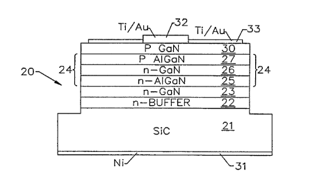
diode such as the one broadly designated at 20 in
Figure 1. The double heterostructure light emitting
diode 20 illustrated in Figure 1 emits in the blue
portion of the visible spectrum and comprises a
substrate 21 preferably formed of silicon carbide that
has been sufficiently doped to provide a conductive
substrate for the vertical structure LED 20 illustrated
in Figure 1. In order to match the crystal structure
of the buffer and aluminum gallium nitride layers on
the substrate 21, the silicon carbide substrate has a
polytype preferably selected from the group consisting
of 6H or 4H silicon carbide.
As known by those familiar with these
materials, 4H and 6H are two of the hexagonal crystal
~ Q fnrmg - ~,-F ~i 1 i r-t>_ro c_~a_rhi_t7P ~ a_n_t7 can w_h_i_r~1_~ -gal 1 i
pm nitr ide
(and other Group III nitrides) form hexagonal
polytypes. If cubic (e_g. 3C) silicon carbide is used
as the substrate, however, gallium nitride can also
form a cubic structure.
The LED 20 next includes a buffer layer 22 on
the substrate 21. Appropriate buffer layers are
described in U.S. Patent No. 5,393,993. The buffer
CA 02220031 1997-11-03
WO 96/36080 PCT/L1S96/05160
-10-
structure provides an appropriate crystal and
electronic transition between the silicon carbide
substrate and the double heterostructure portion of the
LED 20.
In one embodiment the buffer layer comprisesa
first layer of gallium nitride and aluminum nitride; '
and a second layer of gallium nitride and aluminum
nitride adjacent to the first layer. The mole
percentage of aluminum nitride in the second layer is
substantially different from the mole percentage of
aluminum nitride in the first layer.
In another embodiment the buffer layer
comprises a conductive layer selected from the group
consisting of gallium nitride, aluminum nitride, indium
nitride, ternary Group III nitrides having the formula
AXB1_,sN, where A and B are Group III elements and where x
is zero, one, or a fraction between zero and one,
quaternary Group III nitrides having the formula AXBYCl_X-
yN' where A, B, and C are Group III elements; x and y,
are zero, one, or a fraction between zero and one, and
1 is greater than (x + y), and alloys-of silicon
carbide with such ternary and quaternary Group III
nitrides.
In yet another embodiment, the buffer layer
comprises a first layer upon the substrate formed of a
graded composition of silicon carbide aluminum gallium
nitride in which the portion adjacent the substrate is
substantially entirely silicon carbide and the portion
furthest from the substrate is substantially entirely
aluminum gallium nitride with the portions therebetween
being progressively graded in content from
predominantly silicon carbide to.predominantly aluminum
gallium nitride. A second layer can be added to the
first layer, and can be formed of a graded composition .
of aluminum gallium nitride_
In preferred embodiments, the LED 20 further
comprises an n-type gallium nitride epitaxial layer 23
CA 02220031 1997-11-03
WO 96/36080 PCT/US96/05160
-11-
on the buffer layer 22 which provides anadditional
crystal transition between the substrate, the buffer,
and the heterostructure.
The LED 20 next includes a double
heterostructure indicated by the brackets 24 in Figure
1. The double heterostructure 24 includes an n-type
layer of aluminum gallium nitride 25 which, when the n-
type gallium nitride epitaxial layer 23 is included in
the structure, rests upon the n-type gallium nitride
epitaxial layer 23. The n-type layer 25 of aluminum
gallium nitride has the formula AlXGa1_,~N, where x
designates the mole fraction of aluminum, and where 1
is greater than x and x is greater than 0 (1>x>0). In
preferred embodiments the mole fraction x is between
about 0.05 and 2.0, and in the most preferred
embodiments, the mole fraction x is about 0.1. The
aluminum gallium nitride layer 25 furthermore has a net
doping density of about 2E18 and is doped with silicon
in the most preferred embodiments_ As commonly used in
this art, "E" is an abbreviated exponential notation
for dopant density, so that 2E18 represents 2x1018cm-3.
The double heterostructure 24 includes an
active layer 26 of gallium nitride on the n-type
aluminum gallium nitride layer 25 which, as noted
above, is compensated with a Group II acceptor and a
Group IV donor, and in which the preferred Group II
acceptors are zinc or cadmium or magnesium, and in
which carbon can comprise a Group IV acceptor. The
preferred Group IV donor is silicon or germanium. In
the most preferred embodiments, the Group II acceptor
is zinc, and the Group IV donor is silicon as these
produce the characteristic blue emission described
herein with respect to a number of the other drawings.
The net doping density of theactive layer26is
between about 1E18 and 4E18, and most preferably about
2E18.
CA 02220031 1997-11-03
WO 96/36080 PCT/US96/05160
-12-
The double heterostructure is completed with
a p-type aluminum gallium nitride layer 27 which has
the formula
AlXGa1_,~N where one is greater than x and x is greater
S than 0 (1>x>0), and in which the preferred mole
fraction x is also between about 0.05 and 2.0, and most
preferably about 0.1.
In preferred embodiments, the LED 20 can
further comprise a p-type gallium nitride layer 30 on
the top p-type layer 27 of the heterostructure. The p-
type layer 27 has a net doping density of about 1E19
and is preferably doped with aluminum.
The LED 20 illustrated in Figure 1 further
comprises respective ohmic contacts 31 to the substrate
and 32 to the top layer; i.e. to the p-type gallium
nitride layer 30 in the embodiment illustrated in
Figure 1. It will be understood, however, that in
embodiments that do not include the p-type gallium
nitride layer 30, the ohmic layer 32 is made directly
to the p-type aluminum gallium nitride layer 27 of the
double heterostructure.
Figure 1 also illustrates that in preferred
embodiments, the contact 32 comprises a bonding pad of
titanium and gold. In a most preferred embodiment, the
contact is formed from a thin layer of titanium (Ti)
overlaid with a layer of gold (Au). In a preferred
embodiment, the basic contact 32 is accompanied by a
transparent ohmic contact 33 which extends across a
larger portion of the top surface of the LED 20 to help
spread current and thus increase brightness.
A preferred ohmic contact to the silicon
carbide substrate comprises nickel, but can also
comprise other appropriate metals or metal combinations
such as nickel-vanadium.
The double heterostructure light emitting
diode 20 illustrated in Figure 1 will consistently
produce an emission with a peak wavelength of about 430
CA 02220031 1997-11-03
R'O 96/36080 PCT/LTS96/05160
-13-
nanometers (nm) and a bandwidth at half maximum of
about 65 nm when a typical LED current (for example
between 10 and 40 milliamps) is applied across the p-n
junction that is formed by the aluminum gallium nitride
layer 27 of the heterostructure and the gallium nitride
' active layer 26 of the heterostructure 24.
Figure 2 shows a slightly different
embodiment of an LED 40 according to the present
invention. In Figure 2, the substrate is shown at 41,
and the buffer layer is shown at 42, but which in this
embodiment comprises an insulating buffer layer. As
noted earlier herein, the buffer layer can comprise the
structure disclosed in U.S. Patent No. 5,393,993.
Alternatively, the buffer layer 42 can comprise a
graded layer of AlGaN that is substantially entirely
aluminum nitride where it meets the substrate 41, and
then is progressively graded with increasing amounts of
gallium until it is substantially entirely gallium
nitride at its upper surface where it meets the n-type
layer of gallium nitride shown as 43 in Figure 2 and as
23 in Figure 1.
The double heterostructure is illustrated at
44 in Figure 2 and in a preferred embodiment comprises
the n-type aluminum gallium nitride layer 45 that
otherwise corresponds to the layer25 described with
respect to Figure 1, a compensated n-type gallium
nitride active layer 46 which likewise corresponds to
the gallium nitride active layer 26 described with
respect to Figure 1, and a p-type aluminum gallium
nitride layer 47 which similarly corresponds to the
layer 27 described with respect to Figure 1_ A p-type
gallium nitride layer 50corresponding to layer 30 in
Figure 1 is on the heterostructure, and the ohmic
. contacts 51 to the substrate and 52 and 53 to the top
of the diode correspond to those described as 31, 32,
and 33 in Figure 1_
CA 02220031 1997-11-03
WO 96/36080 PCTIUS96/05160
-14-
As Figure 2 illustrates, however, because the
buffer layer 42 in this embodiment is insulating rather
than conductive, some other path for current flow must
be provided between the ohmic contact 51 on the
substrate and the ohmic contacts 52 and 53 on the top
layer of the diode. This contact is made through
shorting contacts 54 and 55 which are preferably formed
on aluminum or titanium and aluminum and which provide
an ohmic contact to the n-type gallium nitride layer
43. In the most preferred embodiments, these shorting
contacts further include portions illustrated at 56 and
57 that are in immediate contact with the n-type
silicon carbide substrate and which are formed of
titanium and nickel to produce an appropriate ohmic
contact with the silicon carbide.
In another aspect, the invention comprises a
method of producing an active layer of compensated
gallium nitride for a double heterostructure light
emitting diode that emits in the blue portion of the
visible spectrum. In this ripect, the invention
comprises introducing vaporized sources of gallium,
nitrogen, silicon and zinc into a chemical vapor
deposition system that includes a semiconductor
substrate compatible with the growth of gallium nitride
thereon. The temperature is maintained high enough to
promote the epitaxial growth of zinc and silicon
compensated gallium nitride, but lower than the
temperature at which the gallium nitride would
decompose. As is well understood by those of ordinary
skill in this art, the temperature must be high enough
to provide the energy required to get atoms to move
across the epitaxial growth surface, and in preferred
embodiments of the present invention, this temperature
is generally maintained between about 800°C and 1050°C. ,
It will be further understood by those of
ordinary skill in this art, that gas flow rates and
specific temperatures are generally system-dependent,
CA 02220031 1997-11-03
WO 96/36080 PCT/US96/05160
-15-
and thus specific temperatures and the like other than
those recited herein will fall within the method
aspects of the invention because they can be easily
determined for particular chemical vapor-deposition
("CVD") systems by those of ordinary skill in this art
and without undue experimentation.
As another limiting factor, the temperature
is preferably maintained lower than the temperature at
which the surface morphology ofthe epitaxial layer
would become unacceptable for further epitaxial growth
thereon.
In preferred embodiments, the step of
introducing the vaporized source of gallium comprises
introducing trimethyl gallium, (CH3)3Ga; the step of
introducing a vaporized source of nitrogen comprises
introduces ammonia, NH3; the step of introducing a
vaporized source of zinc comprises introducing dimethyl
zinc, (C2H5)2Zn; and the step of introducing a vaporized
source of silicon comprises introducing silane, SiH4.
The preferred aluminum source (for the AlGaN layers) is
trimethyl aluminum, (CH3)3A1; and when magnesium is
introduced, the preferred source is biscyclopentadienyl
magnesium, (CSHS) 2Mg.
Figure 3 is an SEM photograph of an LED
according to the present invention. Such a device has
a chip size of about 14 mil x 14 mil, with a 10 mil x
10 mil mesa portion. The substrate is about 7 or 8
mils thick, the n-GaN layer (e_g. 23 in Figure 1 or 43
in Figure 2) is about 3 microns thick and the layers in
the heterostructure (n-AlGaN, GaN, and p-AlGaN ) are
each about 1000 angstroms (A) thick. The top GaN layer
(e. g. 30 in Figure 1 and 50 in Figure 2).is about 4000A
thick.
Figures 4-14 illustrate various performance
characteristics of the layers that make up the
heterostructure and heterostructure diode according to
the present invention. Figure 4 illustrates the
CA 02220031 1997-11-03
WO 96/36080 ' PCT/ITS96/05160
-16-
spectral response of a gallium nitride double
heterojunction light emitting diode formed on a silicon
carbide substrate according to the present invention as
a function of operating current. Figure 4 shows
measurements made at four different currents between 10
and 40 milliamps (mA). Thepeak emission wavelength is
430 nanometers (nm) with a bandwidth at half maximum of
about 60 nanometers which is characteristic of the
silicon and zinc compensated gallium nitride active
layer.
Figure 5 illustrates the power output and
external quantum efficiency of a light emitting diode
according to the present invention as a function of
operating current. As a normal operating current for
such an LED (i.e. approximately 20 milliamps), the
output is approximately 850 microwatts which
corresponds to an external quantum efficiency of about
1.50.
Figure 6 illustrates the room temperature
photoluminescence of various combinations of aluminum
gallium nitride on silicon carbide substrates and also
including a pure gallium nitride layer for comparative
purposes. The clean, well defined peaks that are
measured at room temperature demonstrate the high
crystal quality of these layers. These
photoluminescent measurements were made by exciting the
layers with a 10 milliwatt helium/cadmium laser at 328
nanometers.
Figure 7 demonstrates the current voltage
characteristics of ohmic contacts made to n-type
gallium nitride on silicon carbide substrates according
to the present invention. The preferred ohmic contact
metal is aluminum which yields a contact resistance of
about 10-5 ohm-cmz for an n-type gallium nitride layer
with a donor density of about 1018cm-3.
Figure 8 is a similar current voltage plot
demonstrating the characteristics of ohmic contacts
CA 02220031 1997-11-03
R'O 96/36080 PCT/US96/05160
-17-
made to p-type -g~llii~.fti nitride Lori s-ilicon carbide
substrates according to the present invention. The
preferred ohmic contact metal is an alloy of titanium
and gold which yields a contact resistance of
approx-imately 10-2 ohms-cm2 for a p-type acceptor
density o'f approximately 6E17 in the gallium nitride
layer.
Figure 9 is the current voltage (I-V) curve
for-a. gallium nitride double heterojunction light
emitting diode on silicon carbide according to the
present invention. In reverse bias no leakage current
is detected_ Under forward bias the LED begins to turn
on at about 2.7 volts and exhibits an operating voltage
of about 3.7 volts at a typical current of 20
milliamps.
Figure 10 illustrates the room temperature
photoluminescence ofmagnesium doped p-type gallium
nitride on silicon carbide. The peak occurs at about
435 nanometers for a layered doped to a net acceptor
concentration of about 6E17.
Figure 11 is a partial logarithmic plot of
Hall effect data showing the carrier concentration and
resistivity of an n-type gallium nitride as a function
of temperature, plotted inversely to temperature. The
layer from which the measurements for Figure 11 were
taken was doped with silicon to a net donor
concentration of about 1.4E18 and had a resistivity of
0.016 ohm-centimeter at room temperature.
Figure 12 is corresponding data for the same
layer as illustrated by Figure 11, but demonstrating
mobilityfor the layer. The mobility of the layer is
approximately 300 cm2/V~s at room temperature, a high.
value for this doping level indicating the high quality
nature of the layer.
Figure 13 is a plot of Hall effect data
showing the acceptor concentration and resistivity of
magnesium doped gallium nitride as a function of
CA 02220031 1997-11-03
R'Q 96/36080 PCTJUS96/05160
-18-
temperature (plotted inversely). The net acceptor
concentration for this layer was about 6E17 and showed
a resistivity of about 1.3 ohms-centimeter at room
temperature_ -
Figure 14 illustrates the corresponding
mobility data for the same layer as Figure 13 and '
illustrates that the mobility of the layer is
approximately 8 cm2/V~s at room temperature which is
typical of the mobility of p-type gallium nitride.
In the drawings and specification, there have
been disclosed typical preferred embodiments of the
invention and, although specific terms have been
employed, they have been used in a generic and
descriptive sense only and not for purposes of
limitation, the scope of the invention being set forth
in the following claims.