Note: Descriptions are shown in the official language in which they were submitted.
CA 02220~47 1997-11-10
DESCRIPTION
SEMICONDUCTOR MEMORY HAVING ARITHMETIC FUNCTION AND
PROCESSOR USING THE SAME
Technical Field
The present invention relates to a display
apparatus for performing pixel density conversion
processing such as enlargement, reduction, and rotation on
an original image and displaying a resultant image or to an
image processing apparatus and, more particularly, to a
processing apparatus for performing a high-speed filtering
operation such as data interpolation, which is pixel
density conversion processing, and to a memory having
arithmetic function for use in the high-speed filtering
operation.
Background Art
A conventional display apparatus for performing
enlargement, reduction, and rotation on an image is used in
texture mapping apparatuses such as disclosed in Japanese
Non-e~;ned Patent Publication Nos. Hei 5-298455 and Hei
5-307610. In these publications, methods are disclosed in
which, since the coordinate value of an original image
corresponding to its destination does not match the center
CA 02220~47 1997-11-10
of a pixel of the original image, the value of the pixel of
a specified coordinate is estimated by interpolation of
pixels around the specified pixel. For enlargement of a
binary character image, Japanese Non-e~m;ned Patent
Publication No. Sho 59-6626 discloses a method of obt~ining
destination pixels fast enlarged from plural pixels of an
original image. In addition, for image differentiation and
integration in image processing, a method is well known in
which a product-sum operation is performed by weighting
surrounding eight pixels.
The conventional processing apparatus such as
mentioned above for reading plural pixels from an original
image for arithmetic operations has plural memory devices
and arithmetic units arranged in parallel to perform
parallel processing for high-speed processing.
However, when arranging plural memory devices and
reading data at high speeds from an original image for
processing, the above-mentioned prior-art technologies
present a problem of significantly increasing the number of
signal lines between the processor for performing that
processing and the plural memory devices. For example, if
one pixel consists of 24 bits (red, green, and blue
consisting of eight bits each) and an arithmetic operation
is performed from an original image consisting of four
pixels, 96 bits of data lines are required. Data reading
CA 02220~47 1997-11-10
performance of a memory device itself, if the same is an
ordinary random access memory, is currently limited to 150
ns in a random access operation. In order to achieve a
target performance, this access speed must be further
increased by parallel processing, which in turn increases
the number of signal lines still further. This inevitably
increases equipment scale as well as equipment cost because
the individual performance (operating frequency) needs to
be increased.
Disclosure of Invention
It is therefore an object of the present invention
to provide a processing apparatus capable of performing
high-speed processing by decreasing the number of signal
lines between a higher processor and memory devices and
provide a semiconductor memory having arithmetic function
for use in this processing apparatus.
Another object of the present invention is to
provide a plurality of semiconductor memories having
arithmetic function and a processing apparatus for
processing an original image which is too large to be
stored in a single semiconductor memory having arithmetic
function.
In carrying out the invention and according to one
aspect thereof, there is provided a semiconductor memory
CA 02220~47 1997-11-10
-- 4 --
having arithmetic function comprising: a storage means for
holding data corresponding to continuous integer addresses;
a fraction address holding means for holding an integer
component and a fraction component constituting a fraction
address inputted from a processor; an arithmetic means for
reading data corresponding to the integer component and
data before or after the data from the storage means and,
by use of the read data and the fraction component held in
the fraction address holding means, interpolating data
corresponding to the fraction address; and an address range
determining means for determining whether an address is
within a range of the addresses of the data held in the
storage means, all of the above-mentioned means being
formed on a single LSI chip.
In carrying out the invention and according to
another aspect thereof, there is provided a processing
apparatus using a semiconductor memory having arithmetic
function comprising: a processing processor for generating
an address including a fraction component as instructed
from a higher processor; and a plurality of semiconductor
memories having arithmetic function having a storage means
for holding data corresponding to continuous integer
addresses and an arithmetic means for obtaining, for the
address including a fraction component inputted from the
processing processor, data corresponding to the address
CA 02220~47 1997-11-10
including a fraction component by use of the data
corresponding to continuous integer addresses held in the
storage means and the fraction component of the address;
wherein each of the plurality of semiconductor memories
holds part of data of an adjacent memory in the storage
means in a mutually overlapped manner.
Conventionally, an address is outputted to plural
memory devices for one coordinate, about four to 16 pixels
around that coordinate are read, which are captured by the
higher processor, and the higher processor performs
arithmetic processing by using the values of the captured
pixels. Therefore, it is required to transfer about four
to 16 pixels of data between the memory device and the
higher processor in order to generate output data of one
pixel.
According to the present invention, the above-
mentioned arithmetic processing is performed inside the
LSI, so that the data of only one pixel may be transferred
between the semiconductor memory having arithmetic function
and the higher processor in order to generate output data
of one pixel. Inside the semiconductor memory having
arithmetic function, about four to 16 pixels of data is
still transferred; but, in the actual memory device, data
of several thousand bits (in the case of a 16 Mb DRAM, 16
Rbits for example) can be read simultaneously and more
CA 02220~47 1997-11-10
6 --
pixel data can be read. As for access time for memory
cells, it is necessary to drive a signal line of at least
10 PF in order to output data to the outside of a chip.
Inside the LSI, at most only 1 PF of capacitance may be
driven, thereby enabling high-speed access to memory.
Further, according to the present invention, a
fraction address inputted from the processor is
interpolated by use of data corresponding to the integer
address held in the above-mentioned storage means to obtain
data corresponding to the fraction address. The following
specifically describes the linear interpolation for one-
dimensional data sequence. If the value of coordinate A =
10 being 100.0 and the value of coordinate A = 11 being
130.0 are stored in memory, the value of coordinate A =
10.6 can be interpolated by multiplying the value of
coordinate A = 11 by 0.6 and multiplying the value of
coordinate A = 10 by 0.4 and adding the multiplication
results together = 118Ø Thus, the interpolation output
can be obtained by uniquely determining, in coordinate
fraction component, a weight coefficient to be multiplied
by each pixel and adding the multiplication results
together.
Still further, according to the present invention,
a plurality of semiconductor memories having arithmetic
function are provided that has a storage means for holding
CA 02220~47 1997-11-10
data corresponding to continuous integer addresses and an
arithmetic means for obtaining data corresponding to the
address including a fraction component by use of the data
corresponding to continuous integer addresses held in the
storage means and the fraction component of the address
from the address including the fraction component inputted
from the processing processor, wherein each of the
plurality of semiconductor memories holds part of data of
an adjacent memory in the storage means in a mutually
overlapped manner. Therefore, if the size of an original
image is too large to be stored in one LSI chip, such a
large memory space is divided into plural areas and each of
these areas can be allocated to each of the plural
semiconductor memories having arithmetic function. In
addition, part of data is held in an overlapped manner, so
that the data in the proximity of the boundary between the
divided areas can be well processed.
Brief Description of Drawings
FIG. 1 is a block diagram illustrating a
semiconductor memory having arithmetic function practiced
as one embodiment of the present invention;
FIG. 2 is a diagram illustrating some functions of
the semiconductor memory having arithmetic function;
FIG. 3 is a diagram illustrating a processing
CA 02220~47 1997-11-10
apparatus using a plurality of semiconductor memories
having arithmetic function;
FIG. 4 is a block diagram illustrating an input
data buffer block shown in FIG. 1;
FIG. 5 is a block diagram illustrating a command
processing block shown in FIG. 1;
FIG. 6 is a block diagram illustrating a pixel
processing block shown in FIG. 1;
FIG. 7 is a block diagram illustrating a memory
cell shown in FIG. 1; and
FIG. 8 is a block diagram illustrating an output
data buffer block shown in FIG. 1.
Best Mode for Carrying out the Invention
The following describes one embodiment of the
present invention with reference to drawings.
Referring to FIG. 2, there are shown some functions
of a semiconductor memory having arithmetic function
practiced as one embodiment of the present invention.
First, FIG. 2 (a) illustrates an example of interpolating a
one-dimensional data sequence in a linear (linear equation)
manner. The horizontal axis represents addresses while the
vertical axis represents data values corresponding to the
addresses. Each vertical bar represents the value set in
memory while the lines connecting the bars at their tops
CA 02220~47 1997-11-10
represent interpolated output. Namely, if the data
sequence is stored at addresses O through 15 in the
semiconductor memory having arithmetic function according
to the present invention, specifying an address having a
fraction component and reading the data from that address
allows reading of linearly interpolated data from before
and after the data specified by the address. For example,
if 128 is stored at address 9 and 166 at address 10 and a
read operation is performed by specifying 9.87 as an
address, the semiconductor memory having arithmetic
function reads two addresses 9 and 10, which are nearest to
the address 9.87, from the memory and interpolates the
values of the addresses 9 and 10 by fraction component 0.87
of the specified address, outputting an interpolation
result. For linear interpolation, let the integer
component of an address be Ti and its fraction component be
Tf, then interpolation result ip can be obtained from
expression (1), so that, in the above-mentioned example,
161 is outputted.
ip - A(Ti) x (1 - Tf) + A(Ti + 1) x Tf ... (1)
where, A(x) indicates the value stored at the specified
address. Next, FIG. 2 (b) illustrates an example in which
the data sequence is interpolated quadratically. For
linear interpolation, data between two pieces of data is
calculated. For quadratic interpolation, interpolation is
CA 02220~47 1997-11-10
-- 10 --
performed from the values of continuous three addresses, so
that the values can be varied smoothly as shown in the
figure. The calculation for the interpolation can be
performed by following expression (2) obtained by solving
an equation.
ip = (A(Ti - 1) x (Tf - 1) x Tf
+ 2 x A(Ti) x (1 - Tf) x (1 + Tf)
+ A(Ti + 1) x (1 + Tf) x Tf)/2 ... (2)
If address 9 is 128, address 10 is 166, and address
11 is 40 and a read operation is performed with an address
being 9.87, since the three addresses nearest to address
9.87 are 9, 10, and 11, Ti = 10, Tf = -0.13, so that ip =
170.
FIG. 2 (c) illustrates an example in which a
quadratic data sequence is interpolated and an
interpolation result is outputted. It is assumed that the
memory be accessible by quadratic addresses (coordinates)
and data (pixel) for each addresses be eight bits. In the
figure, the value of eight pixels of which X and Y
coordinates are (2,3), (3,3), (4,3), (5,3), (6,3), (4,4),
(4,5) and (4,6) is set to 255 and the other pixels are set
to 0. If X - 3.4 and Y = 4.8 are specified and this
semiconductor memory having arithmetic function is read,
values of pixels of which coordinates are (3,4), (3,5),
(4,4), and (4,5) are read for interpolation and an
-
CA 02220~47 1997-11-10
interpolation result is outputted in the case of linear
interpolation. If the integer parts and the fraction parts
of the coordinates X, Y to be read are TXi, TXf and TYi,
TYf, then interpolation result ip can be obtained from
expression (3).
ip = A(TXi,TYi) X (1 - TXf) x (1 - TYf)
+ A(TXi + l,TYi) X TXf x (1 - TYf)
+ A(TXi,TYi + 1) 2 (1 - TXf) x TYf
+ A(TXi + l,TYi + 1) X TXf x TYf ... (3)
Therefore, in the example of FIG. 2 (c), ip = 102.
FIG. 2 (d) illustrates an example in which a three-
dimensional data sequence is interpolated and an
interpolation result is outputted. This figure shows an
example of linear interpolation. The semiconductor memory
having arithmetic function uses eight pixels around a
specified coordinate (a dot in the figure) and an offset
(dx, dy, dz) from an integer grid to perform interpolation
in the same manner as those of the above-mentioned one-
dimensional and two-dimensional interpolating operations.
So far, the capability of the semiconductor memory
having arithmetic function has been described with
attention mainly paid to linear interpolation. Like the
above-mentioned expression (2), a weight coefficient for
data can be obtained from the fraction component of an
address to interpolate values by such higher-degree
CA 02220~47 l997-ll-lO
- 12 -
functions as quadratic and cubic. Further, if the obtained
weight coefficient is fixed, a Laplacian filter can be
implemented.
The following describes an internal constitution of
the semiconductor memory having arithmetic function with
reference to FIG. 1.
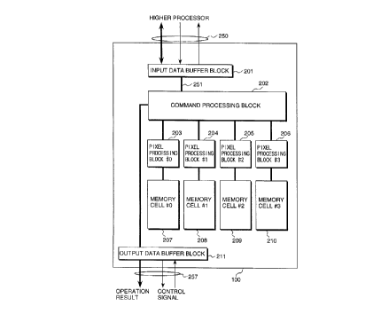
A semiconductor memory having arithmetic function
100 comprises an input data buffer block 201 that receives
an address, write data, and control-signal transmitting
signal line group 250 from a higher processor and buffers
an access request coming from the higher processor, a
command processing block 202 that receives the buffered
access request from the higher processor sent over the
signal line group 251, decodes the request, converts the
decoded requests into actual memory addresses to control
the access of pixel processing blocks 203, 204, 205, and
206 for performing parallel processing for each pixel, and
instructs these blocks to perform interpolation, the pixel
processing blocks 203, 204, 205, and 206 that reads memory
according to the instruction issued from the command
processing block 202 to multiply pixel data by a weight
coefficient, memory cells 207, 208, 209, and 210 that
actually store data, and an output data buffer block 211
that receives a result of the interpolation performed by
the command processing block to output the result to
CA 02220~47 1997-11-10
outside of the chip.
To interpolate a two-dimensional image, the higher
processor stores two-~im~n~ional image data to be stored
via the signal line group 250. Next, selection between
linear interpolation, quadratic interpolation, and use of a
fixed weight coefficient is set to a MOD register (not
shown). Then, when an address (coordinates) to be read is
set from the signal line group 250, the command processing
block 202 calculates addresses to be given to the four
pixel processing blocks 203, 204, 205, and 206 and obtains
a weight coefficient for each pixel from the fraction
component of the specified address. Next, the four pixel
processing blocks 203, 204, 205, and 206 read the pixel
data of the specified addresses, multiply the pixel data by
the specified weight coefficient and return multiplication
results to the command processing block 202. The returned
multiplication results are added together and an addition
result is outputted to the higher processor as the read
data via an output data buffer.
The following describes a constitution of a
processing apparatus for performing high-speed processing
of a large amount data by use of this sem.iconductor memory
having arithmetic function with reference to FIG. 3. FIG.
3 illustrates a part of an image processing apparatus for
performing arithmetic processing based on a two-dimensional
CA 02220~47 l997-ll-lO
- 14 -
original image. A processing processor 10 generates a
coordinate of an pixel as instructed from a higher CPU and
accesses semiconductor memories having arithmetic function
100, 101, 102, and 103 for reading. In a graphics display
apparatus for example, this processing processor 10 holds
texture mapping data in the semiconductor memories having
arithmetic function 100, 101, 102, and 103, generates a
texture data coordinate for every pixel from the coordinate
values corresponding to the vertexes of a triangle, reads
interpolated pixel information, and writes this information
to a frame memory (not shown). The outline of this
processing is disclosed in the above-mentioned Japanese
Non-examined Patent Publication No. Hei 5-298455.
In FIG. 3, an original image 20 is too large to be
stored in one semiconductor memory having arithmetic
function. Therefore, the image is divided into four areas
with the boundaries overlapped as shown. The processing
processor generates an address (coordinates) larger than a
space of data stored in each of the memories for access, so
that the semiconductor memories having arithmetic function
100, 101, 102, and 103 determine whether output can be made
to the respective specified addresses. As a result of the
determination, only the semiconductor memory having
arithmetic function of which output data is valid is
enabled to output interpolation output to a read data bus
CA 02220~47 1997-11-10
151. To specify which of the areas each semiconductor
memory having four arithmetic functions 100, 101, 102, 103
are to be related to, a dedicated signal line is provided
for each semiconductor memory having arithmetic function.
Alternatively, this specification may be made by providing
an internal register for area det~r~ination. The following
briefly describes an operation of the processing apparatus
that uses a plurality of semiconductor memories having
arithmetic functions 100, 101, 102, 103 as shown in FIG. 3.
The processing processor 10 outputs an address signal
including a fraction component and a control signal to the
semiconductor memories having arithmetic function from an
MEMC terminal. When each semiconductor memory having
arithmetic function has obtained an interpolation result
for the specified address, the memory outputs a signal
indicating the end of the processing to an SA terminal and
the interpolation result to an SO terminal. However, since
only one semiconductor memory having arithmetic function is
read for the request address from the processing processor,
the SA terminals of the other semiconductor memories having
arithmetic function are ~valid~ and the SO term; n~l S of
these memories are put in a high-impedance state. The
processing processor reads the read data bus 151 if the
result of an AND operation between the outputs of the SA
terminals of all memories having arithmetic function is
CA 02220~47 l997-ll-lO
- 16 -
"valid," asserts an MEMR terminal after completion of the
reading, and requests next data output. Thus, the reading
can be performed from the processing processor in a
pipeline manner.
The following describes an internal constitution of
the semiconductor memory having arithmetic function with
reference to FIGS. 4 through 8.
FIG. 4 illustrates an internal constitution of the
input data buffer block 201. The input buffer block 201 is
largely composed of a PBIO (Processor Buffer Interface) 212
for receiving an access request from the higher processor
and decodes the received request and a FIFO (First In, Fast
Out) buffer 213 for buffering the access request. There
are four types of accesses to be requested from the higher
processor: direct memory access for accessing memory like
an ordinary linear address; register access for reading and
writing a register internal to the semiconductor memory
having arithmetic function; two-~;m~n~ional write access
for writing a memory cell in two-~;m~ional space; and
interpolation read access for reading interpolation data by
specifying a two-dimensional coordinate having a fraction
component. Basically, these accesses are classified by
address spaces to be specified.
First, the signal line group 250 between the higher
processor and the PBIO will be described. A signal line AD
CA 02220~47 1997-11-10
provides a signal for transmitting an address and data, a
signal line ADSEL provides a signal indicating which of the
address and data is set to the signal line AD, a signal
line RW provides a signal indicating read access when high
and write access when low, a signal line CLR provides a
clock signal, a signal line WAIT provides a signal
indicating access enable, and a signal line CSEL provides a
signal indicating that an access request is valid.
Negt, a procedure in which the higher processor
performs direct memory access will be described. First,
the higher processor specifies the signal line ADSEL, sets
memory address information of direct memory access of which
most significant two bits are "00" for example for
accessing the signal line AD, sets the signal line RW to
high level in a read operation, and sets the signal line
CSEL to the access enabled state. When the signal line CLR
rises with the signal line WAIT in the access enabled
state, a read access operation of direct memory access
starts and the access information is stored in the FIFO
213. Then, the content of the FIFO 213 is read by the
command processing block 202 and after the pixel processing
block reads data from a memory cell, the read data is
inputted in the PBIO 212 of the input data buffer block 201
via a signal line RDT. On the other hand, when the higher
processor sets the data to the signal line ADSEL after
CA 02220~47 1997-11-10
address setting, the signal line AD shifts to a state in
which the data is outputted from the semiconductor memory
having arithmetic function. By reading the data on the
signal line AD at a cycle in which the read data comes, the
read operation comes to an end. This cycle in which the
read data comes is determined by a m~i m~lm time of memory
cell reading. The cycle is ten and several clocks. This
direct memory access is for use in memory check.
Therefore, this direct memory access does not especially
require a high-speed operation, presenting no problem in
the above-mentioned access procedure. The write access of
the direct memory access is implemented by writing the
signal line RW in the above-mentioned read access. The
signal value of the signal line AD with the address set is
captured, in the input state, into the PBIO 212 and stored
in the FIFO 213 as write data. At this moment, the access
by the higher processor comes to an end. Subsequently, in
the memory having arithmetic function, this access
information is taken by the command processing block out of
the FIFO 213 and written to the corresponding memory cell
via the pixel processing block.
In register access, access can be made by giving a
register space in which the most significant two bits of an
address to be specified are "01" for example. When viewed
from the higher processor, read access and write access are
CA 02220~47 1997-11-10
-- 19 --
generally the same except that there is no direct memory
access and no waiting time for read data. On the other
hand, in the input data buffer block, a register access
request is not stored in the FIFO 213 and a register write
signal RWE, a register address ADR, and write data WDT are
generated to directly control the actual register.
Two-~ n~ional write access is performed in the
same manner as the write operation in direct memory access.
When an address is set, the most significant two bits of
the address signal are set to "10" for example and the X
and Y coordinates are set to the subsequent bits.
In interpolation read access, which is like two-
dimensional write access, read access is specified with the
signal line RW at high level. For the address to be
specified, the most significant two bits of the address
signal are set to "11" for example and the X and Y
coordinates are set to the subsequent bits. However, this
interpolation read access differs from the other access
methods in that the interpolated read data is read from the
signal line 250 and written to the higher processor,
thereby allowing the next cycle with an address set to
continuously set an address. Therefore, unless the FIFO
213 is stuffed up, access operations can be performed
continuously, realizing high-speed access.
The following describes the operation of the FIFO
CA 02220~47 l997-ll-lO
- 20 -
213. First, when performing access to the FIFO 213 of the
above-mentioned four types of access operations, the PBIO
outputs data to be written to the FIFO 213 to the signal
line WDT and a signal for instructing a write operation to
the FIFO 213 to a signal line WTF. At this moment, if the
FIFO 213 iS full, a signal line WTA issues an access
disabled signal and therefore the FIFO 213 does not accept
the write operation. The data to be stored in the FIFO 213
includes an address of direct memory access, data at the
write operation, an address and data for two-dimensional
write access, an address of interpolation read access, and
information for identifying these addresses and data. If
any one piece of these data is stored in the FIFO 213, a
signal line EMP is negated, upon which data of the first
access request is outputted to a signal line FDT. To read
this data, the command processing block 202 asserts a
signal line FRD. This asserts the signal line EMP when the
FIFO 213 iS emptied, notifying the command processing block
that there is no access request to be outputted.
The following describes the command processing
block 202 with reference to FIG. 5.
The command processing block 202 receives an access
request from the input data buffer block 201, perform
arbitration with a refresh cycle request unique to the
dynamic memory, controls the pixel processing blocks 203,
CA 02220~47 l997-ll-lO
- 21 -
204, 205, and 206, calculates read data, and outputs the
obtained read data to the output data buffer block.
The command processing block 202 incorporates a
refresh control block for periodically outputting a request
signal RR for refreshing a memory cell, which is a dynamic
memory, a request processing block 214 for performing
arbitration between an access request from the input data
buffer block 201 and a refresh request from the refresh
control block 215 and processing each of these requests in
one to several steps, an address processing block 216 for
calculating an address to be given to the pixel processing
block from the address (coordinates) coming from the
request processing block 214 and the type of access and
determining whether that coordinate can be calculated from
the data stored in the memory cell of the address
processing block, a filter coefficient calculating block
218 for calculating from the fraction component of the
address a weight coefficient to be multiplied by a pixel, a
pixel arithmetic control block 217 for controlling the
pixel processing blocks 203, 204, 205, and 206 by the
address coming from the address processing block 216 and
the weight coefficient coming from the filter coefficient
calculating block 218, and an arithmetic block 219 for
performing an arithmetic operation on the data obtained by
multiplying the pixels outputted from the pixel processing
CA 02220~47 1997-11-10
blocks 203, 204, 205, and 206 by the weight coefficient and
sending its result to the output data buffer.
First, the refresh control block 215 calculates
time in synchronization with the clock and outputs a
refresh request signal RR about every 10 ~s.
The request processing block 214 knows by the
signal line EMP that an access request has come to the
input data buffer block 201, thereby capturing the access
request on the signal line FDT. At the same time, by
asserting the signal line FRD, the request processing block
can put a next access request onto the signal line FDT.
Also, the request processing block 214 receives the above-
mentioned refresh request signal RR to know that refresh is
necessary. First, when the request processing block 214
receives a refresh request signal RR in the idle state, the
request processing block counts up an internal refresh
counter and outputs the count and a flag indicating the
refresh request to a signal line RXY. If there is no
refresh request and the signal line EMP is not asserted,
the request processing block takes the access request from
the signal line FDT and stores the access request into an
internal access request register. Then, the request
processing block operates as follows according to each
access request. First, when a read request of direct
memory access comes, the request processing block outputs a
CA 02220~47 1997-11-10
- 23 -
specified address and a flag of the read request of direct
memory access to the signal line RXY. When a write request
of direct memory access comes, the request processing block
outputs a specified address and a flag of the write request
of direct memory access to the signal line RXY and outputs
write data to the signal line RXY in the next cycle. The
write data at this point is stored in the FIFO 213 next to
the write address. In two-dimensional write access, the
request processing block outputs a specified coordinate and
a flag of a two-~;m~ional write access request to the
signal line RXY and outputs write data to the signal line
RXY in the next cycle. For interpolation read access, the
request processing block outputs a specified coordinate and
a flag of interpolation read access request to the signal
line RXY. At this point, since there are four pixel
processing blocks, if four pixels are read for processing,
the processing can be made without change; however, if 16
pixels are read for processing for example, control is
performed such that the 16 pixels are processed in units
four pixels from top to down. To do so, the flag of
interpolation read access request includes a value that
indicates a number of four-pixel group. In this
processing, one interpolation read access is completed in
four cycles.
The address processing block 216 knows by the
CA 02220~47 l997-ll-l0
- 24 -
access request flag on the signal line RXY that there is a
request, performs address conversion and output to the
pixel arithmetic control block 217 accordingly. First, if
the access request flag on the signal line RXY indicates a
refresh request, the address processing block 216 outputs
the address (counter value) and the flag to a signal line
CXY without change. The signal line CXY includes access
request flag signal lines for the four pixel processing
blocks and signal lines for address or data transmission.
When issuing a refresh request, the address processing
block outputs the refresh request to all signal lines of
the four pixel processing blocks in the same manner. Next,
if the access request flag on the signal line RXY indicates
a direct memory access read operation, the address
processing block outputs the address and the flag to the
signal line CXY connected to the pixel processing block to
which the memory cell corresponding to the specified
address is connected. If the access request flag indicates
a direct memory access write operation, the address
processing block outputs the address and the flag to the
signal line CXY connected to the pixel processing block to
which the memory cell corresponding to the specified
address is connected and outputs write data in the next
cycle. If the access request flag on the signal line RXY
indicates a two-dimensional write access operation, the
CA 02220~47 l997-ll-lO
- 25 -
address processing block outputs the address and the flag
to the signal line CXY connected to the pixel processing
block to which the memory cell corresponding to the
specified address is connected and, at the same time,
outputs write data in the next cycle. If the access
request flag on the signal line RXY indicates an
interpolation read access operation, the address processing
block transfers the fraction part of the address (
coordinates) to the filter coefficient calculating block
218 via a signal line FRC and, at the same time, outputs
the address and the flag corresponding to each pixel
processing block to the signal line CXY. As described
above, for interpolation requiring to read more than four
pixels, the address processing block outputs the address
and the flag to the signal line CXY while changing the
addresses corresponding to the pixel processing blocks.
The following shows a relationship between the
memory addresses and the coordinates in direct memory
access, two-dimensional write access, and interpolation
read access. First, the memory addresses are continuously
provided in the order of memory cells 207, 208, 209, and
210. Coordinates (o~o) correspond to address 0 of the
memory cell 207, coordinates (0,1) correspond to address 0
of the memory cell 208, coordinates (1,0) correspond to
address 0 of the memory cell 209, coordinates (1,1)
CA 02220~47 l997-ll-lO
- - 26 -
correspond to address O of the memory cell 210, and
coordinates ( 2,0) correspond to address 1 of the memory
cell 207. Thus, a pixel of which X coordinate is an even
number and Y coordinate is an even number corresponds to
the memory cell 207, a pixel of which X coordinate is an
even number and Y coordinate is an odd number corresponds
to the memory cell 208, a pixel of which X coordinate is an
odd number and Y coordinate is an even number corresponds
to the memory cell 209, and a pixel of which X coordinate
is odd number and Y coordinate is an odd number corresponds
to the memory cell 210. As with the processing apparatus
of FIG. 3 in which the plurality of semiconductor memories
having arithmetic function are used by dividing an area,
the above-mentioned relationship between addresses and
coordinates is relatively the same with offsets attached.
Namely, address O of the memory 207 corresponds to
coordinates ( 512,0) and address O of the memory cell 208
corresponds to coordinates (512,1) for example. These
offset values are determined by a signal (not shown) that
performs chip area specification, is directly set from
outside of the LSI, and is used in the address processing
block 216. When the processing apparatus is composed of a
plurality of semiconductor memories having arithmetic
function such as mentioned above, the address processing
block 216 determines where the data for interpolating
CA 02220~47 1997-11-10
specified coordinates is located in its own memory cell.
If the interpolation is found practicable, the address
processing block outputs an access request to the pixel
processing block 217 via the signal line CXY as described
above and, at the same time, outputs a signal RF indicating
the output of the access request to the arithmetic block
219. If the interpolation is found impracticable, the
address processing block outputs a signal NRF indicating
that the access request is disabled for arithmetic
operation to the arithmetic block 219. The determination
whether the above-mentioned data for interpolation is
located in own memory cell can be easily implemented by a
comparator.
The filter coefficient calculating block 218
calculates a weight coefficient to be multiplied by each
pixel in interpolation read access. To be more specific,
the filter coefficient calculating block calculates weight
coefficients shown in the above-mentioned expressions (1),
(2), and (3) from the fraction part of coordinates and
outputs the calculated coefficients to the pixel arithmetic
control block via a signal line COEF. The processing for
o~t~i n i ng weight coefficients can easily be implemented by
a multiplier and an adder. Interpolation by a cubic
expression requires division by three. In this case, too,
the processing can be implemented by multiplication of a
CA 02220~47 l997-ll-lO
- 28 -
constant of 1/3. If the number of digits of a fraction
part is small, a coefficient can be obtained by table
reference by stored coefficients in memory. Without using
the fraction part of coordinates, a Laplacian filter can be
implemented in the same procedure as interpolation read
access by providing a register for holding a Laplacian
filter coefficient.
The pixel arithmetic control block 217 distributes
addresses from the address control block 216 for the pixel
processing blocks 203, 204, 205, and 206, a flag indicating
the type of access, and a weight coefficient COEF for use
at interpolation read access to the pixel processing blocks
203, 204, 205, and 206.
The arithmetic block 219 receives the signal RF
indicating that a read request has been outputted and,
after passing of a certain time, captures read data RDT0
through 3 from the pixel processing blocks 203, 204, 205,
and 206 to add the data together. The arithmetic block
outputs the addition result to a signal SDT and sets to a
signal SWT that the addition result is ~valid" and ~'the
addition result is outputted from the semiconductor memory
having arithmetic function.~ If the output data buffer
block is stuffed up and therefore no more data can be
accepted, a signal SFULL is asserted, so that, at that
moment, the state of the arithmetic block 219 must not be
CA 02220~47 1997-11-10
- 29 -
changed. Normally, "valid" is set to the SWT, upon which a
next arithmetic operation can be started. To perform
interpolation from 16 pixels, the addition result is
internally held and the output is made at the fourth time,
making the SWT "valid.~ If the signal NRF indicating no
interpolation output is asserted in this LSI, the
arithmetic result is uncertain and therefore the SWT is set
to "valid" and "the interpolation result is not outputted
from the semiconductor memory having arithmetic function."
The above-mentioned description is related to an
example of interpolation read access. In the case of
direct memory access read, the corresponding one from the
read data RDT 0 through 3 is outputted to the RDT according
to the signal RXY including the specified coordinates.
The following describes the pixel processing block
203 with reference to FIG. 6.
First, a signal PPC0, which is the input to the
pixel processing bloc, is composed of an address indicating
coordinates, a flag indicating an access type, a weight
coefficient, and write data for data write access. In
every access mode, an address is stored in an address
register 220 first and converted by a memory control unit
into a memory cell address, which is outputted with a
control signal to a signal line MADC. In interpolation
read access, a weight coefficient is stored in a
- - -
CA 02220~47 1997-11-10
- 30 -
coefficient register 223. In direct memory access write
and two-dimensional write access, the data to be written
after the address is set to the PPC0, so that this write
data is stored in a data register.
When a certain time passes after the memory control
unit 221 outputs a data read request from a memory cell,
the read data is set to a read signal line MRDT. This time
is determined by the address for the memory cell. If the
address of the data currently read to a sense amplifier 229
is specified, the read data is set after one clock. If the
address of data not in the sense amplifier 229 is
specified, the read data is set after six clocks.
The read data is multiplied in a multiplier 224 by
the value of the coefficient register and the result is
passed to the command processing block 202 via a signal
RDT0. The pixel processing blocks 204, 205, and 206 have
the same constitution as the pixel processing block 203
because the command processing block 202 accesses each
pixel processing block with differences in operation taken
into consideration.
The following describes the memory cell 207 with
reference to FIG. 7.
The memory cell 207 is composed of a register WA
230 for storing address data on the signal MADC, a storage
element 2 33 arranged on a two-dimensional grid, an X
CA 02220~47 1997-11-10
decoder 232 for selecting one row of storage elements 233,
a sense amplifier 229 for reading data of one row of
storage elements 233 and storing the read data, a Y decoder
for selectively reading and writing one pixel of data
stored in the sense amplifier according to the address held
in the register WA230, and a control circuit 231 for
controlling the X decoder 232, the sense amplifier 229, and
the Y decoder 228 according to the control signal on the
signal MADC.
The memory cell shown is the same as the cell of an
ordinary dynamic memory and not a special memory cell. The
control signal on the signal MADC can be specified with an
operation for reading one row of storage elements 233
selected by the X decoder into the sense amplifier 229, an
operation for capturing one pixel of data from the data
located on the sense amplifier 229 and outputting the
captured data to the signal MRDT, an operation for writing
the value of a signal MWDT of write data to the sense
amplifier 229, and an operation for writing the data of the
sense amplifier 229 selected by the X decoder to one row of
storage elements 233. According to these specifications,
the control circuit 231 controls the X decoder 232, the
sense amplifier 229, and the Y decoder 228.
The following describes the output data buffer
block 211 with reference to FIG. 8.
CA 02220~47 1997-11-10
The SDT signal, which is data about an
interpolation result coming from the command processing
block 202, is stored in a buffer BUFF 240 along with flag
"output from the semiconductor memory having arithmetic
function" according to the "valid" flag indicated by the
SWT. This buffer BUFF 240 is a FIFO. Therefore, if no
more data can be stored therein, a SFULL signal is
asserted. If the buffer BUFF 240 contains data, the buffer
asserts a signal RDA and outputs valid data to a BDT and
the flag "output from the semiconductor memory having
arithmetic function" to a signal OE. When a data update
signal UP comes from an output block SBIO 241, the buffer
outputs the buffered data to the signals BDT, RDA, and OE.
The output block SBIO 241 is a simple LSI input/
output driver. When the OE is asserted, the output block
outputs the value of the signal BDT to a signal line SO;
when the OE is negated, the output block puts the signal
line SO into high-impedance state. Signal lines SA and SR
are connected to the RDA and the UP without change via a
driver.
Lastly, a processing apparatus for processing a
large image by use of a plurality of semiconductor memories
having arithmetic function will be described with reference
to FIG. 3.
In what follows, an example of image enlargement
CA 02220~47 1997-11-10
processing will be shown. First, image data 20 of an
original image to be enlarged is stored in the
semiconductor memories having arithmetic function 100, 101,
102, and 103 by the higher CPU via the processing
processor. At this point, the processing processor 10
gives an integer address (coordinates) and then its data to
the signal terminal MEMC in two~ n~ional write access,
thereby setting the pixel of the image data 20 of the
original image to the semiconductor memory having
arithmetic function. At this point, each semiconductor
memory having arithmetic function determines by the address
processing block 216 whether the area is its own area. If
the area is found its own area, the semiconductor memory
having arithmetic function performs write access from the
pixel arithmetic control block 217 to the corresponding
memory cell. The relationship between this semiconductor
memory having arithmetic function and the image data 20 of
the original image is a slightly large area than each of
the equally divided areas of the image data 20 of the
original image as shown by the extension line drawn from
the semiconductor memory having arithmetic function of Fig.
3. Namely, each semiconductor memory having arithmetic
function has, in an overlapped manner, pixels around the
boundary between the divided areas of the image data 20 of
the original image. The size of the overlapped area
CA 02220~47 1997-11-10
- 34 -
depends on the degree of interpolation. In interpolation
by a linear expression, the size is one pixel. In
interpolation by quadratic and cubic expressions, the size
is two pixels. Thus, each semiconductor memory having
arithmetic function can read the pixels of an original
image for interpolation inside its own LSI.
The following describes the processing for reading
given coordinates of the image data 20 of an original
image. The processing processor 10 gives an address
(coordinates) having a fraction component to the signal
ter~; n~l MEMC in interpolation read access. This address
can be obtained by sequentially adding about 0.77, which is
the reciprocal number of 13 if the image is to be enlarged
thirteen fold for example. The address thus obtained can
be given continuously until a WAIT signal of a signal line
group ADC is asserted. Meanwhile, if this interpolation
read access is made, the semiconductor memory having
arithmetic function causes the address processing block 216
of the command processing block 202 to determine whether
the specified address is the address to be outputted by the
semiconductor memory having arithmetic function as
described before and outputs the in~erpolation result to
the output data buffer block 211. If the address is the
address to be outputted by the semiconductor memory having
the arithmetic function, the SA terminal of the same is
CA 02220~47 1997-11-10
- 35 -
asserted upon obt~;n;ng of the interpolation result. If
the address is not the address to be outputted, the SA
terminal is asserted once for each interpolation read
access. The signal of the SA term;n~l is connected to a
MEMA terminal of the processing processor 10, through an
AND gate, by which the processing processor 10 can know
that the read result for one interpolation read request has
been established. If the processing processor 10 captures
this data to request a negt interpolation read result,
asserting a MEMR terminal connected to the SR terminal of
each semiconductor memory having arithmetic function
outputs the next interpolation read result to the SO
terminal.
Repeating the above-mentioned processing provides
the pixel data of a new image resulted from enlarging the
image data 20 of the original image. The new image thus
obtained is written by a ter~; n~l not shown of the
processing processor to the image memory to be displayed on
a CRT or the like.
As described and according to one embodiment,
memory access is made inside the LSI chip, so that, if the
number of signal lines connected to the higher processor is
equal to the signal frequency, the processing speed is
increased four times, four being the degree of memory
access parallelism, namely the number of pixel processing
CA 02220~47 1997-11-10
blocks. Inside the LSI, the processing speed increases
still further because of small wiring capacitance.
Conversely, to implement the same performance by a prior-
art constitution, parallelism of more than four times is
required, thereby increasing the equipment size and cost.
The pixel processing blocks having a multiplier in
units of pixels are provided and multiplication is
performed in parallel, thereby enabling interpolation for
image reduction and enlargement at a high speed.
If a plurality of semiconductor memories having
arithmetic function are used in order to handle a large
image, a circuit is provided for determining that a
slightly smaller area than the area of an image stored in
each semiconductor memory having arithmetic function is the
area to be outputted by that semiconductor memory having an
arithmetic function. By this novel constitution, an
address space larger than the address space of actually
stored data and a small address space between adjacent
pieces of data can be set when the semiconductor memories
having arithmetic function are viewed from the upper
processor.
Thus~ the present embodiment has been described
mainly with respect to enlargement and reduction of a two-
dimensional image. It will be apparent that the same
effect can be obtained by the same constitution with
CA 02220~47 1997-11-10
respect to a three-dimensional image and a four-dimensional
image (the fourth dimension may be time axis or the four-
dimensional image may be a plurality of prefiltered three-
dimensional images).
By use of the constitution briefly described with
reference to the present embodiment, image processing such
as the Laplacian filter can be performed.
As described and according to the present
invention, an address having fraction component may be
specified to the data stored at an integer address, thereby
providing the data interpolated at a high speed.
By holding the data of a larger address space than
the address space outputted by one semiconductor memory
having arithmetic function, data interpolated at a high
speed and a low cost may be provided for the data of a huge
address space by use of a plurality of semiconductor
memories having arithmetic function.