Note: Descriptions are shown in the official language in which they were submitted.
CA 02220592 1997-11-10
OPTICAL PATH SIGNAL TERMINATION EQUIPMENT
Background of the Invention
Field of the Invention
The present invention relates to techniques for accommodating synchronous
digital hierarchy (SDH) signals in an optical path network. It relates in
particular to
conversion between SDH signals transmitted at the electrical level and optical
path
signals transmitted at the optical level.
Description of Related Ai-t
Wavelength division multiplexing (WDM) techniques, which make full use of
the broadband nature of light, and optical path networks, which introduce
wavelength
routing into the path layer, have both been undergoing rapid development. It
might be
assumed that existing SDH, ATM and PDH (plesiochronous digital hierarchy)
networks will all be accommodated in optical path networks. However, PDH
networks
are currently being replaced by SDH networks, and the majority of ATM networks
are
SDH-based systems which accomniodate ATM cells in SDH paths. Therefore, the
central task is the accommodation of SDH signals in optical path networks.
FIG.1 serves for a simple explanation of a conventional switched network
connecting subscriber terminals. Subscribers 11 and 18 are connected via
switch 12,
transit switch 13, line terminators 14 and 15, transit switch 16, and switch
17.
Subscriber 11 and switch 12 are connected by, for example, a 64 kb/s channel,
as are
switch 17 and subscriber 18. Switch 12, transit switch 13 and line terminator
14 (and
line terminator 15, transit switch 16 and switch 17) are connected by, for
example, 52
Mbit/s paths comprising time division multiplexed 64 kb/s channels.
Transmission
CA 02220592 1997-11-10
2
between line terminators 14 and 15 involves further multiplexing of these
paths.
FIG.2 serves to explain the connection of SDH signal paths via an SDH path
cross-connect. Transit switches 21-1 to 21-4 are respectively connected to SDH
path
cross-connect 25 via line terminators 22-1 to 22-4 and 23-1 to 23-4. FIG.2
shows a
single path from transit switch 21-1 to each of transit switches 21-2 to 21-4,
and in
general transmission between line terminators 22-1 to 22-4 and 23-1 to 23-4 is
carried
out on the basis of time division multiplexed paths, with the direction of
individual
paths being set by SDH cross-connect 25.
FIG.3 serves to explain how some of the path connections shown in FIG.2 are
realized in an optical path network. In this case, optical path terminators 26-
1 to 26-3
are used instead of line terminators, and these optical path terminators 26-1
to 26-3 are
each connected to optical path cross-connect 27 via wavelength division
multiplexed
links. Optical paths can be established as desired between optical path
terminators 26-
1 to 26-3, and these optical paths are accommodated in the wavelength division
multiplexed links using WDM techniques. A detailed account of such optical
path
networks is given in, for example, K. Sato and S. Okamoto, "Evolution of Path
Layer
Techniques Toward Photonic Networks", IEICE Japan Autumn Meeting, September
1992, SB-7-1, and K. Sato, S. Okamoto, and H.Hadama, "Optical Path Layer
Technologies to enhance B-ISDN performance", Proc.IEEE ICC'93, June 1993,
pp. 1300-1307.
An optical path signal comprises a main signal and an optical path supervisory
signal. Two types of signal are used as the supervisory signal. The first type
is an
optical path supervisory signal which is multiplexed at the electrical level
in the same
CA 02220592 2006-08-24
3
frequency band as the main signal. This type is primarily used for supervising
the
quality of the main signal. The second type is an optically added optical path
supervisory signal which is multiplexed at the optical level in a different
frequency
band from the main signal or is superimposed to the main signal by a
modulation
separate from that used for the main signal. This second type is primarily
used for
management and identification of the type of main signal. (See S. Okamoto, K.
Oguchi and K. Sato, "Network architecture and management concepts for optical
transport networks", Proceedings on IEEE/IFIP 1996 Network Operations and
Management Symposium (NOMS '96), pp.1-11, April 1996, and Japanese Patent 08-
049751-A, "Method for supervision of wavelength multiplexed optical
communications").
Thus, when an optical path signal is wavelength multiplexed and transmitted
through WDM links, an optical path supervisory signal and a wavelength
multiplexed
optical path supervisory signal are transmitted along with it, these
supervisory signals
being contained in part of the optical path signal. The optical path
supervisory signal
and the wavelength multiplexed optical path supervisory signal are monitored,
and if
a fault occurs in an optical fibre or some transmission equipment, path
restoration is
performed by re-establishing the optical path along a route which detours
around the
location of the fault.
An explanation will now be given of the SDH transmission scheme. In SDH
transmission, the unit of information transfer is the virtual container (VC),
which
comprises payload (information to be transmitted) and a "path overhead" which
is
added to this payload. When VC signals are to be accommodated in a
transmission
CA 02220592 1997-11-10
4
medium such as an optical fibre, a frame called a "synchronous transfer
module"
(hereinafter, STM) is formed. An administrative unit (AU) signal is formed by
firstly
adding pointers (AU pointers) to the VC signals in order to manage differences
in the
alignment of the VC signals with respect to the STM frame, and then time
division
multiplexing the VC signals. An STM-N signal is formed by time division
multiplexing N of these AU signals and adding a section supervisory signal.
After
electrical to optical conversion of this STM-N signal, it is sent to the
optical fibre. The
reverse processing is carried out at a receiving terminal (see ITU-T
Recommendation
G.707, "Digital transmission system - Terminal equipments - General" and ITU-T
Recommendation G.783, "Characteristics of synchronous digital hierarchy (SDH)
equipment functional blocks"). When SDH signals are transmitted in wavelength
multiplexed form, a plurality of STM-N sign are transmitted after being
converted to
optical signals of different wavelengths.
When a fault occurs somewhere in the transmission medium or in some
transmission equipment, path restoration is performed by re-routing VCs around
the
location of the fault. It is stipulated that when a fault occurs, the
termination
equipment adjacent to the fault location maintains alignment with respect to
the frame
by generating STM-N or VC signals in which every bit is a logical "1" and
using these
as a substitute for the lost signal. In this case, because the SDH path
supervisory
signals in the VCs will not have valid values, faults can be detected in
individual VCs
and succeeding VCs re-routed.
The conventional signal format for accommodating an SDH signal in an optical
path network will be explained with reference to FIG.4 to FIG.7. FIG.4 shows
the
CA 02220592 1997-11-10
format of a VC signal, FIG.5 the format of an STM-N signal, FIG.6 the format
of an
AU signal, and FIG.7 the format of an optical path signal. In these signal
format
diagrams, the direction of time elapse is from left to right along the
horizontal axis. In
addition to being read from left to right, the signals are also read
vertically, so that
5 reading starts at the top left of the frame and finishes at the bottom right
(all subsequent
drawings showing signal format will follow this pattern).
Different sizes of virtual container are defined, each capable of
accommodating
a different transmission rate. These different VCs are laiown as VC-1i, "VC-
12, VC-:,
VC-3, VC-4, VC-4-4c and VC-4-16c. FIG.4 shows the format of a VC-4 signal. It
will be seen that this comprises a 260x9 byte payload area P and a 9 byte path
supervisory signal area P0. An STM-N signal comprises multiplexed VC signals
of
this sort. More precisely, as shown in FIG.5, an STM-N signal has a 9x(261xN)
byte
payload area, a 3x(9xN) byte section supervisory signal area Si, a 5x(9xN)
byte
section supervisory signal area S2, and a 1x(9xN) byte AU pointer area a.
The signal format of a conventional optical path signal differs from that of
an
STM-N signal in the SDH transmission scheme. It is therefore necessary, when
transferring an SDH signal through an optical communication network, to
convert the
SDH signal format to an optical path signal format.
Namely, when an STM-N signal is to be accommodated in an optical path, the
signal has to be made longer and its transmission speed increased so that, as
shown in
FIG.7, an optical path supervisory signal area can be provided and an optical
path
supervisory signal inserted therein.
There is also the problem that when a fault occurs within the optical
CA 02220592 2006-08-24
6
communication network, two kinds of path restoration are required, namely,
alternative
routing of optical paths within the optical communication network, and
alternative
routing of VC signals in the SDH. As a result, increased network resources are
needed.
The present invention has been devised in the light of this situation, and it
is an
object of this invention to provide optical path signal termination equipment
capable
of inserting an optical path supervisory signal without increasing signal
length.
Summary of the Invention
According to a first aspect of the invention, there is provided optical path
signal
termination equipment having: electrical signal termination means (121-124,131-
134,
141) for terminating one or more SDH ("synchronous digital hierarchy") signals
which
have been transmitted by electrical signals, and for outputting an electrical
signal for
sending to the optical path; and optical path termination means (211-214) for
inserting
an optical path supervisory signal at the electrical level into this
electrical signal,
converting the resulting signal into an optical signal, and outputting this as
the optical
path signal; wherein the optical path termination means comprises means (211)
for
inserting the aforementioned optical path supervisory signal in place of the
SDH
section supervisory signal contained in the SDH signal which the electrical
signal
termination means has terminated.
The electrical signal termination means preferably comprises: one or more
means for respectively processing the SDH section supervisory signal or
signals
contained in the one or more SDH signals; one or more demultiplexing means for
respectively demultiplexing the SDH signal or signals thus processed, thereby
CA 02220592 1997-11-10
7
converting it or them to a plurality of VC signals; and multiplexing means for
multiplexing the plurality of VC signals output by this or these
demultiplexing means,
converting them to AU signals by adding AU pointers, further multiplexing the
plurality of AU signals thus obtained, and outputting an electrical signal
with an optical
path signal format. The insertion means preferably inserts the aforementioned
optical
path supervisory signal at the electrical level in a predetermined area of
this electrical
signal with an optical path signal format. In particular, it preferably
inserts the optical
path supervisory signal at the electrical level in an area which corresponds
to the area
for the SDH section supervisory signal in the SDH signal format (termed the
"section
overhead").
It is feasible to provide a plurality of optical path termination means, to
provide
a multiplexing means in correspondence with each of these plurality of optical
path
termination means, and to provide between these multiplexing means and the
aforementioned demultiplexing means a switching circuit for switching signals.
It is
also feasible to provide a plurality of multiplexing means and optical path
termination
means, but for the switching circuit for switching signals to be provided
between the
outputs of the multiplexing means and the inputs of the optical path
termination
means.
The optical path termination means preferably includes means for adding to the
optical path signal an optical path supervisory signal at the optical level,
this signal
being separate from the optical path supervisory signal at the electrical
level. This
adding means may be configured to wavelength division multiplex the optical
path
signal and the optical path supervisory signal at the optical level, or it may
be
CA 02220592 1997-11-10
8
configured to apply to the optical path signal a modulation separate from that
used for
the main signal.
According to a second aspect, this invention is optical path signal
termination
equipment for use as the receiving terminal of an optical path terminator. As
such, it
comprises: an optical path termination means for receiving an optical path
signal and
converting it to an electrical signal; and an electrical signal termination
means for
converting the electrical signal output by this optical path termination means
to one or
more SDH signals and outputting this or these; wherein the optical path signal
has a
signal format which does not contain the SDH section supervisory signal of the
SDH
signal, and the electrical signal termination means includes one or more means
which
respectively insert an SDH section supervisory signal in place of the optical
path
supervisory signal contained in the optical path signal received by the
optical path
termination means.
The optical path termination means preferably includes means which, after the
optical path signal has been converted to an electrical signal, extracts the
optical path
supervisory signal at the electrical level which has been added to the
predetermined
area of the electrical signal. The electrical signal termination means
preferably
includes: demultiplexing means for demultiplexing the electrical signal output
by the
optical path termination means, thereby converting it to a plurality of VC
signals;
multiplexing means for converting the plurality of VC signals output by this
demultiplexing means to AU signals by multiplexing them and adding AU
pointers;
and means for respectively adding SDH section overheads to the AU signals
output by
these multiplexing means.
CA 02220592 1997-11-10
9
The optical path supervisory signal at the electrical level is added to the
optical
path signal in the area of the SDH section supervisory signal in the SDH
signal format.
The optical path termination means can be configured to output an electrical
signal
with an optical path signal format, said electrical signal containing this
optical path
supervisory signal at the electrical level. The electrical signal termination
means can
also comprise: demultiplexing means for demultiplexing the electrical signal
output by
the optical path termination means (said electrical signal including the
optical path
supervisory signal at the electrical level), thereby converting to a plurality
of VC
signals; means for respectively rewriting the SDH path supervisory signal
areas
contained in the plurality of VC signals output by this demultiplexing means;
multiplexing means for multiplexing the outputs of these rewriting means and
converting them to AU signals by adding AU pointers; and means for adding SDH
section supervisory signals to the AU signals output by these multiplexing
means.
It is feasible to provide a plurality of optical path termination means, to
provide
a demultiplexing means in correspondence with each of these plurality of
optical path
termination means, and to provide between these demultiplexing means and the
aforementioned multiplexing means a switching circuit for switching signals.
It is also
feasible to provide a plurality of optical path termination means and a
plurality of
demultiplexing means, but for the switching circuit for switching signals to
be provided
between the outputs of this plurality of optical path termination means and
the inputs
of the plurality of demultiplexing means.
The optical path termination means preferably includes means for separating
from the optical path signal the optical path supervisory signal at the
optical level, this
CA 02220592 1997-11-10
signal being separate from the optical path supervisory signal at the
electrical level.
An optical path terminator can have a plurality of the aforementioned optical
path
signal termination equipment for use as transmitting terminals, and can be
provided
with wavelength multiplexing means which allocates an optical carrier of
different
5 wavelength to each of this plurality of optical path signal termination
equipment,
wavelength division multiplexes their respective output optical signals, and
sends the
result to the optical transmission line. An optical path terminator can also
have a
plurality of the aforementioned optical path signal termination equipment for
use as
receiving terminals, and can be provided with wavelength demultiplexing means
which
10 allocates an optical carrier of different wavelength to each of this
plurality of optical
path signal termination equipment, demultiplexes the wavelength multiplexed
optical
signal from the optical transmission line, and outputs the results to the
plurality of
optical path signal termination equipment.
Brief Description of the Drawings
FIG.1 serves as a simple explanation of a conventional switched network
connecting subscriber terminals.
FIG.2 serves to explain path connection of SDH signals via an SDH cross-
connect.
FIG.3 serves to explain how some of the path connections shown in FIG.2
would be implemented in an optical path network.
FIG.4 shows the format of a VC signal.
FIG.5 shows the format of an STM-N signal.
CA 02220592 1997-11-10
11
FIG.6 shows the format of a conventional AU signal.
FIG.7 shows the format of a conventional optical path signal.
FIG.8 is a block diagram of optical path signal termination equipment
according
to a first embodiment of the present invention.
FIG.9 shows the format of an optical path signal according to this invention.
FIG.10 shows an example of a configuration for superimposing an optical path
supervisory signal at the optical level on an optical path signal.
FIG.11 shows an example of aiiother configuration for superimposing an opiical
path supervisory signal at the optical level on an optical path signal.
FIG.12 is a block diagram of optical path signal termination equipment
according to a second embodiment of this invention.
FIG.13 is a block diagram of optical path signal termination equipment
according to a third embodiment of this invention.
FIG.14 is a block diagram of optical path signal termination equipment
according to a fourth embodiment of this invention.
FIG.15 is a block diagram of optical path signal termination equipment
according to a fifth embodiment of this invention.
FIG.16 is a block diagram of optical path signal termination equipment
according to a sixth embodiment of this invention.
FIG.17 is a block diagram of optical path signal termination equipment
according to a seventh embodiment of this invention.
FIG.18 is a block diagram of an optical path terminator according to an eighth
embodiment of this invention.
CA 02220592 1997-11-10
12
FIG. 19 is a block diagram of an optical path terminator according to a ninth
embodiment of this invention.
Detailed Description of Preferred Embodiments
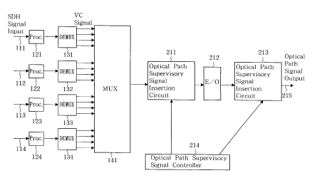
The configuration of a first embodiment of this invention will be explained
with
reference to FIG.8 and FIG.9. FIG.8 is a block diagram showing optical path
signal
termination equipment according to the first embodiment, while FIG.9 shows the
format of an optical path signal according to this invention.
This embodiment is used as a transmitting terminal of an optical path
terminator.
In order to terminate one or more SDH signals which have been transmitted by
electrical signals, and output an electrical signal for sending to an optical
path, it
comprises: input lines 111-114 at which the SDH signals arrive; SDH section
supervisory signal processing circuits 121-124 for terminating these SDH
signals and
processing the SDH section supervisory signals contained therein;
demultiplexing
circuits 131-134 for demultiplexing the outputs of these SDH section
supervisory
signal processing circuits 121-124, thereby converting them to a plurality of
VC
signals; and multiplexing circuit 141 for converting the plurality of VC
signals output
from these demultiplexing circuits 131-134 to AU signals by multiplexing them
and
adding AU pointers, and then further multiplexing the plurality of AU signals
thereby
obtained and outputting an electrical signal in optical path signal format. In
addition,
in order to convert this electrical signal to an optical signal for output to
the optical
path, this embodiment comprises a first optical path supervisory signal
insertion circuit
211 for inserting an optical path supervisory signal at the electrical level
in place of the
CA 02220592 1997-11-10
13
SDH section supervisory signal contained in the SDH signal; electrical to
optical
conversion circuit 212 for converting to an optical signal the electrical
signal in optical
path signal format to which an optical path supervisory signal at the
electrical level has
been added; a second optical path supervisory signal insertion circuit 213 for
adding
to the optical path signal an optical path supervisory signal at the optical
level which
is separate from the optical path supervisory signal at the electrical level;
and optical
path supervisory signal controller 214 for controlling the addition and
multiplexing of
optical path supervisory signals by the first and second optical path
supervisory sigr.ai
insertion circuits 211 and 213.
As shown in FIG.5, the SDH signals (i.e., STM-N signals) input to SDH signal
input lines 111-114 each comprise 9x(270xN) bytes of data, which is subdivided
into
the following areas: section supervisory signal area S1 (3x(9xN) bytes),
section
supervisory signal area S2 (5x(9xN) bytes), AU pointer area a (lx(9xN) bytes),
and
payload area P(9x(261xN) bytes. SDH section supervisory signal processing
circuits
121-124 perform the processing required to read the data of section
supervisory signal
areas S1 and S2. This processing is defined in ITU-T Recommendation G.708,
"Network node interface for the synchronous digital hierarchy".
The SDH signals processed by SDH section supervisory signal processing
circuits 121-124 are input to demultiplexing circuits 131-134. Each
demultiplexing
circuit 131-134 demultiplexes an STM-N signal into N signals, from each of
which it
extracts and outputs just the payload area P (the VC signal) (9x261 bytes). In
the
example illustrated, an STM-4 signal is input to each of SDH signal input
lines 111-
114, which means that four payload signals (VC signals) are output from each
CA 02220592 1997-11-10
14
demultiplexing circuit 131-134.
The payload signals demultiplexed by demultiplexing circuits 131-134 are input
to multiplexing circuit 141. Multiplexing circuit 141 adds AU pointers to the
sixteen
payload signals that have been input. As shown in FIG.6, the format of a
signal to
which AU pointers have been added (i.e., an AU signal) comprises four areas:
undefined area U1, undefined area U2, AU pointer area a, and payload area P.
Multiplexing circuit 141 also performs byte-interleaved multiplexing of the
sixteen AU
signals.
The output of multiplexing circuit 141 is input to optical path supervisory
signal
insertion circuit 211. Optical path supervisory signal insertion circuit 211
inserts, into
the input signal, an optical path supervisory signal that has been sent from
optical path
supervisory signal controller 214. The resulting signal is converted from an
electrical
signal to an optical signal by electrical to optical conversion circuit 212.
Optical path
supervisory signal insertion circuit 213 then inserts into this optical signal
an optical
path supervisory signal which has been sent from optical path supervisory
signal
controller 214.
As shown in FIG.9, an optical path signal which is output from optical path
supervisory signal insertion circuit 211 comprises the following four areas:
optical path
supervisory signal areas 01 and 02, AU pointer area a, and payload area P. In
this
example, N, the number of multiplexed VC signals, is sixteen.
In this embodiment, a circuit which multiplexes SDH signals is used as
multiplexing circuit 141. As a result, the optical path signal has the format
of an SDH
signal, apart from the fact that an optical path supervisory signal is
inserted instead of
CA 02220592 1997-11-10
an SDH section supervisory signal. This invention can likewise be implemented
using
other formats for the multiplexing carried out by multiplexing circuit 141,
provided that
the signal format used corresponds to this. The important point is that an
optical path
supervisory signal is inserted instead of an SDH section supervisory signal.
5 Electrical to optical conversion circuit 212 is capable of setting different
wavelengths for the output optical signal, and can be implemented for example
by a
tunable wavelength laser. However, it is also feasible to use a fixed
wavelength for the
output optical signal.
As regards the insertion by optical path supervisory signal insertion circuit
213
10 of the optical path supervisory signal at the optical level, an optical
signal of a different
wavelength from the wavelength of the main signal may be used, or a different
modulation from that of the main signal may be applied to the optical path
signal.
Examples of these possibilities are shown in FIG. 10 and FIG. 11. In the
configuration
shown in FIG. 10, a continuous wave output is produced by laser diode 311, and
optical
15 modulator 312 uses the main signal to modulate this continuous wave. In
this case, the
optical path supervisory signal at the optical level can be added by being
superimposed
on the drive signal which is input to laser diode 311. In the configuration
shown in
FIG.11, laser diode 313 is modulated directly by the main signal. In this case
as well,
the optical path supervisory signal at the optical level can be added by being
superimposed on the drive signal which is input to laser diode 313.
FIG. 12 is a block diagram showing optical path signal termination equipment
according to a second embodiment of this invention. The distinguishing feature
of this
second embodiment is that, by adding switching circuit 611 to the first
embodiment,
CA 02220592 1997-11-10
16
the SDH signals can be re-routed.
The operation of SDH signal input lines 111-114, SDH section supervisory
signal processing circuits 121-124, and demultiplexing circuits 131-134 is the
same as
in the first embodiment of this invention.
The payload signals (i.e., VC signals) that have been output from demulti-
plexing circuits 131-134 can have their spatial positions shifted by switching
circuit
611. Because this second embodiment uses a 16x16 switch, it can distribute the
sixteen VC signals in any manner desired between multiplexing circuit 621 and
multiplexing cirquit 622.
The payload signals that have been distributed by switching circuit 611 are
multiplexed by multiplexing circuits 621 and 622. These multiplexing circuits
621 and
622 each add AU pointers to the eight payload signals which have been input.
Multiplexing circuits 621 and 622 also perform byte-interleaved multiplexing
of the
resulting eight AU signals.
The outputs of multiplexing circuits 621 and 622 are respectively sent to
transmitting terminal optical path signal termination circuits 631 and 632.
Transmitting
terminal optical path signal termination circuits 631 and 632 each comprise
optical path
supervisory signal insertion circuit 211, electrical to optical conversion
circuit 212,
optical path supervisory signal insertion circuit 213 and optical path
supervisory signal
controller 214 shown in the first embodiment, and perform the following
processing
on the output of multiplexing circuits 621 and 622 respectively: insertion of
optical
path supervisory signals at the electrical level, electrical to optical
conversion, and
addition of optical path supervisory signals at the optical level. The results
of this
CA 02220592 1997-11-10
17
processing are then output to optical path signal output lines 641 and 642 as
optical
path signals.
Thus, by demultiplexing the input SDH signals into VC signals and providing
a switching circuit capable of switching these VC signals, it is possible to
configure
optical path signal termination equipment which offers a switching function at
the VC
signal level. As a result, in the event of a fault occurring in optical path
signal output
line 641 or 642, the transmission path for the optical path signal can be
rapidly
switched over.
FIG. 13 is a block diagram showing optical path signal termination equipment
according to a third embodiment of this invention. The distinguishing feature
of this
embodiment is that, by employing switching circuit 711 to perform switching
after the
VC signals have been multiplexed, the optical path termination equipment can
be
configured using a smaller switch.
The operation of SDH signal input lines 111-114, SDH section supervisory
signal processing circuits 121-124, and demultiplexing circuits 131-134 is the
same as
in the first embodiment.
The payload signals (i.e., VC signals) which have been output from demulti-
plexing circuits 131-134 are multiplexed by multiplexing circuits 621 and 622.
Namely, multiplexing circuits 621 and 622 each add AU pointers to the eight
payload
signals which have been input, and then perform byte-interleaved multiplexing
of the
resulting eight AU signals.
The signals which have been multiplexed by multiplexing circuits 621 and 622
can have their spatial positions switched by switching circuit 711. Switching
circuit
CA 02220592 1997-11-10
18
711 differs from switching circuit 611 in that it does not switch VC signals,
but instead
switches the output signals from multiplexing circuits 621 and 622.
The outputs of switching circuit 711 are sent to transmitting terminal optical
path signal termination circuits 631 and 632. These transmitting terminal
optical path
signal termination circuits 631 and 632 each comprise first optical path
supervisory
signal insertion circuit 211, electrical to optical conversion circuit 212,
second optical
path supervisory signal insertion circuit 213 and optical path supervisory
signal
controller 214 shown in the first embodiment, and respectively perform the
following
processing on the outputs of switching circuit 711: insertion of optical path
supervisory
signals at the electrical level, electrical to optical conversion, and
addition of optical
path supervisory signals at the optical level. The results of this processing
are then
output to optical path signal output lines 641 and 642 as optical path
signals.
Because this third embodiment uses a 2x2 switch as switching circuit 711, it
can
distribute the SDH signal group input from SDH signal input lines 111 and 112,
and
the SDH signal group input from SDH signal input lines 113 and 114, in any
manner
desired between the two optical path signal output lines 641 and 642. A larger
switch
can be used for switching circuit 711 in correspondence with any increase in
the
number of SDH signal input lines and/or optical path signal output lines. Even
when
a larger switch 711 thus has to be used, it is still possible to employ a
switch with
fewer inputs and outputs than switching circuit 611 used in the second
embodiment.
FIG. 14 is a block diagram showing optical path signal termination equipment
according to a fourth embodiment of this invention, and in particular showing
the
configuration of optical path signal termination equipment for a receiving
terminal
CA 02220592 1997-11-10
19
which converts an optical path signal to SDH signals.
This optical path signal termination equipment comprises: optical path
supervisory signal extraction circuit 812 for separating the optical path
supervisory
signal at the optical level from the optical path signal, optical to
electrical conversion
circuit 813 for converting this optical path signal to an electrical signal,
optical path
supervisory signal extraction circuit 814 for extracting the optical path
supervisory
signal at the electrical level from the optical path signal that has been
converted to an
electrical signal, optical path supervisory signal controller 815 for
processing the
optical path supervisory signals at the optical level and the electrical
level,
demultiplexing circuit 911 for demultiplexing the electrical signal output by
optical
path supervisory signal extraction circuit 814 and converting it to a
plurality of VC
signals, multiplexing circuits 921-924 for multiplexing the plurality of VC
signals
output by this demultiplexing circuit 911 and converting them to AU signals by
adding
AU pointers, and SDH section supervisory signal insertion circuits 931-934 for
inserting SDH section supervisory signals in the AU signals output by these
multiplexing circuits 931-924 and outputting the resulting signals to SDH
signal output
lines 941-944.
Optical path supervisory signal extraction circuit 812 demodulates the optical
path supervisory signal which has been superimposed at the optical level on
the optical
path signal input from optical path signal input line 811. If the optical path
supervisory
signal has been wavelength multiplexed onto the optical path signal, this
demodulation
is performed after wavelength demultiplexing. If the optical path supervisory
signal
has been superimposed by applying a different modulation from that of the
optical path
CA 02220592 1997-11-10
signal, the demodulation is performed after splitting the optical signal. This
enables
the optical path supervisory signal to be demodulated without destroying the
payload
area which constitutes the main signal. The demodulated optical path
supervisory
signal is then sent to optical path supervisory signal controller 815.
5 Optical to electrical conversion circuit 813 converts to an electrical
signal the
optical path signal after it has been processed by optical path supervisory
signal
extraction circuit 812.
Optical path supervisory signal extraction circuit 814 extracts the optical
path
supervisory signal in optical path supervisory signal areas 01 and 02 shown in
FIG.9
10 from the electrical signal output by optical to electrical conversion
circuit 813, and
sends it to optical path supervisory signal controller 815. After this
extraction, optical
path supervisory signal areas 01 and 02 are undefined and may be used to
contain any
kind of data.
Demultiplexing circuit 911 demultiplexes the payload areas of the signal
output
15 from optical path supervisory signal extraction circuit 814 and outputs the
result as
individual VC signals. In this example, it is assumed that demultiplexing
circuit 911
converts its input signal into sixteen VC signals.
Multiplexing circuits 921-924 each multiplex a plurality of VC signals (in
this
case, four) from demultiplexing circuit 911, firstly converting these VC
signals to AU
20 signals by adding AU pointers and then performing byte-interleaved
multiplexing and
outputting the result.
SDH section supervisory signal insertion circuits 931-934 respectively add an
SDH section supervisory signal to the output of multiplexing circuits 921-924,
and
CA 02220592 1997-11-10
21
output the result as an SDH signal to SDH signal output lines 941-944. In this
embodiment, SDH signals are output in the STM-N signal format shown in FIG.5,
with
N=4.
FIG. 15 is a block diagram showing optical path signal termination equipment
according to a fifth embodiment of this invention. This embodiment comprises:
two
optical path signal input lines 1011 and 1012; two receiving terminal optical
path signal
termination circuits 1021 and 1022, each comprising optical path supervisory
signal
extraction circuit 812, optical to electrical conversion circuit 813, optical
path
supervisory signal extraction circuit 814 and optical path supervisory signal
controller
815; and two demultiplexing circuits 1031 and 1032 each similar to
demultiplexing
circuit 911. This fifth embodiment differs from the fourth embodiment in that
it also
has switching circuit 1041 which enables the VC signals converted from the
optical
path signal to be switched.
The operation of receiving terminal optical path signal termination circuits
1021
and 1022 and of demultiplexing circuits 1031 and 1032 is the same as in the
fourth
embodiment. The VC signals output from demultiplexing circuits 1031 and 1032
can
have their spatial positions shifted by switching circuit 1041. Because this
fifth
embodiment uses a 16x16 switch, it can distribute the sixteen VC signals in
any
manner desired among multiplexing circuits 921-924.
The VC signals that have been distributed by switching circuit 1041 are
multiplexed by multiplexing circuits 921-924 in the same manner as in the
fourth
embodiment, and after having SDH section supervisory signals added by SDH
section
supervisory signal insertion circuits 931-934, are output from SDH signal
output lines
CA 02220592 1997-11-10
22
941-944.
Thus, as has been explained above, by demultiplexing the optical path signal
into VC signals and providing a switching circuit capable of switching these
VC
signals, it is possible to configure optical path signal termination equipment
which
offers a switching function at the VC signal level.
FIG. 16 is a block diagram showing optical path signal termination equipment
according to a sixth embodiment of this invention. By performing switching in
switching circuit 1111 prior to demultiplexing into VC signals, this
einbodiinent can
configure the optical path termination equipment using a smaller switch.
The operation of optical path signal input lines 1011 and 1012, and of
receiving
terminal optical path signal termination circuits 1021 and 1022, is the same
as in the
fifth embodiment.
The signals output from receiving terminal optical path signal termination
circuits 1021 and 1022 can have their spatial positions shifted by switching
circuit
1111. Because this sixth embodiment uses a 2 x 2 switch as switching circuit
1111, it
can distribute the optical path signal input from optical path signal input
line 1011 and
the optical path signal input from optical path signal input line 1012 in any
manner
desired between the two SDH signal output line groups (i.e., SDH signal output
lines
941 and 942, and SDH signal output lines 943 and 944).
The signals sent to demultiplexing circuits 1031 and 1032 from switching
circuit
1111 are converted to VC signals. These VC signals are multiplexed by
multiplexing
circuits 921-924, and after having SDH section supervisory signals added by
SDH
section supervisory signal insertion circuits 931-934, are output from SDH
signal
CA 02220592 1997-11-10
23
output lines 941-944.
FIG. 17 is a block diagram showing optical path signal termination equipment
according to a seventh embodiment of this invention. This embodiment
facilitates
flexible network operation by adding SDH path supervisory signal rewriting
circuits
1211-1226 to the fourth embodiment.
The operation of optical path signal input line 811; receiving terminal
optical
path signal termination circuit 821 comprising optical path supervisory signal
extraction circuit 812, optical to electrical conversion circuit 813, optical
path
supervisory signal extraction circuit 814 and optical path supervisory signal
controller
815; and demultiplexing circuit 911, is the same as in the fourth embodiment.
The sixteen VC signals output from demultiplexing circuit 911 are input to
respective SDH path supervisory signal rewriting circuits 1211-1226. In this
patent
application, the VC signals can in principle be any of VC-3, VC-4, VC4-4c and
VC-4-
16c, but the following explanation is for VC-4 signals. As shown in FIG.4, a
VC-4
signal comprises path supervisory signal area PO (9 bytes) and payload area P
(9x260
bytes). SDH path supervisory signal rewriting circuits 1211-1226 are circuits
for
setting a desired value, given from outside, for the path supervisory signal
area PO.
VC signals which have had their path supervisory signal area PO rewritten by
SDH path supervisory signal rewriting circuits 1211-1226 are input to
multiplexing
circuits 921-924, where they are multiplexed. SDH section supervisory signal
insertion
circuits 931-934 are respectively connected to the outputs of multiplexing
circuits 921-
924, and complete the formation of SDH signals by adding SDH section
supervisory
signals, which are then output to SDH signal output lines 941-944.
CA 02220592 1997-11-10
24
Although this seventh embodiment has been configured by adding SDH path
supervisory signal rewriting circuits 1211-1226 to the fourth embodiment, the
same
effect can also be obtained using the configurations of the fifth and sixth
embodiments,
in which a switching circuit was employed, by connecting SDH path supervisory
signal
rewriting circuits 1211-1226 to the outputs of demultiplexing circuits 1031
and
1032.
SDH path supervisory signals are rewritten for example when a fault has
occurred in the optical path signal which is input from optical path signal
input line
811. It is stipulated that if a fault occurs in the optical path signal,
demultiplexing
circuit 911 outputs, as the VC signals, signals in which every bit is a
logical "1" (see
ITU-T Recommendation G.783, "Characteristics of synchronous digital hierarchy
(SDH) equipment functional blocks"). In this event, because the path
supervisory
signal areas of the VC signals do not have a legitimate value, there is a
possibility that
the fault will be recognized by the SDH network and that the path restoration
function
of the SDH network will operate. Because the optical path network also has a
path
restoration function, it is desirable from the point of view of network
operation that
when a fault occurs in the optical path network, paths can be restored without
performing path restoration in the SDH network. Therefore the SDH path
supervisory
signals can be set by the SDH path supervisory signal rewriting circuits in
such manner
that path restoration is not performed in the SDH network.
FIG.18 is a block diagram showing an eighth embodiment of this invention, and
illustrates an example in which the invention has been implemented in an
optical path
terminator to which SDH signals are input and from which a wavelength
multiplexed
CA 02220592 1997-11-10
optical path signal is output to a wavelength multiplex link.
This optical path terminator comprises a plurality of (in this example, three)
optical path signal termination equipment 1421-1423 for terminating the SDH
signals,
converting them to optical path signals, and outputting these. Optical
carriers of
5 different wavelength are allocated to optical path signal termination
equipment 1421-
1423. The optical path terminator of this eighth embodiment also comprises
wavelength multiplexing circuit 1431 which wavelength division multiplexes the
optical signals output from optical path signal termination equipment 1421-
1423 and
sends the result to wavelength multiplex link 1451; and link supervisory
signal
10 insertion circuit 1441 which inserts a link supervisory signal in the
wavelength
multiplexed optical signal sent to wavelength multiplex link 1451 from
wavelength
multiplexing circuit 1431.
In the example of this embodiment, single optical carriers X1 and ~2 are
respectively allocated to optical path signal termination equipment 1421 and
1422,
15 while two optical carriers ~3 and ~4 are allocated to optical path signal
termination
equipment 1423. In this case, the configuration shown in the first embodiment
can be
used for optical path signal termination equipment 1421 and 1422, while the
configuration shown in the second or third embodiments can be used for optical
path
signal termination equipment 1423. Although this eighth embodiment shows a
20 configuration in which a plurality of types of optical path signal
termination equipment
are used together, it is also feasible to have a configuration in which only
one of the
various types of optical path signal termination equipment shown in the
embodiments
is deployed.
CA 02220592 1997-11-10
26
The SDH signals which have been input from SDH signal input lines 1411 are
accommodated in optical path signals by means of optical path signal
termination
equipment 1421-1423. Different wavelengths are allocated to the optical
carriers of
the optical path signals, which are then multiplexed by wavelength
multiplexing circuit
1431. The resulting wavelength multiplexed optical path signal is then input
to link
supervisory signal insertion circuit 1441 and a link supervisory signal is
inserted. This
link supervisory signal is an optical signal which uses an optical carrier of
different
wavelength from the wavelengths of the wavelength multiplexed optical path
signal
group, and is used to transmit information relating to the wavelength
multiplexed
optical path signal group to adjacent optical path termination equipment and
so forth.
In this eighth embodiment, M is used as the optical carrier wavelength for the
link
supervisory signal.
Link supervisory signal insertion circuit 1441 provides the capability of
wavelength multiplexing the link supervisory signal with the already
wavelength
multiplexed optical path signal group. Another possible configuration is to
have
wavelength multiplexing circuit 1431 serve also as the link supervisory signal
insertion
circuit. In either case, the optical path signal group and the link
supervisory signal are
input to wavelength multiplex link 1451.
FIG.19 is a block diagram showing a ninth embodiment of this invention, and
illustrates an example in which the invention has been implemented in an
optical path
terminator which extracts SDH signals accommodated in a wavelength multiplexed
optical path signal input from a wavelength multiplex link, and outputs the
result to
SDH signal output lines.
CA 02220592 1997-11-10
27
This optical path terminator comprises a plurality of (in this example, three)
optical path termination equipment 1541-1543 for terminating the optical path
signals,
converting them to SDH signals, and outputting these. An optical carrier of
different
wavelength is allocated to each optical path termination equipment 1541-1543.
The
optical path terminator of this ninth embodiment also comprises link
supervisory signal
extraction circuit 1521 which extracts the link supervisory signal from the
wavelength
multiplexed optical signal which has been input from wavelength multiplex link
1511;
and wavel;;ngth demultiplexing circuit 1531 which demultiplexes the wavelength
multiplexed optical signal from wavelength multiplex link 1511 and outputs the
results
to optical path termination equipment 1541-1543.
In the example of this embodiment, single optical carriers M and 7~2 are
respectively allocated to optical path signal termination equipment 1541 and
1542,
while two optical carriers ~3 and ~4 are allocated to optical path signal
termination
equipment 1543. In this case, the configuration shown in the fourth or seventh
embodiments can be used for optical path signal termination equipment 1541 and
1542,
while the configuration shown in the fifth or sixth embodiments can be used
for optical
path signal termination equipment 1543. Although this ninth embodiment shows a
configuration in which a plurality of types of optical path signal termination
equipment
are used together, it is also feasible to have a configuration in which only
one of the
various types of optical path signal termination equipment shown in the
embodiments
is deployed.
The wavelength multiplexed optical path signal group and link supervisory
signal are input from wavelength multiplex link 1511 to link supervisory
signal
CA 02220592 1997-11-10
28
extraction circuit 1521. Link supervisory signal extraction circuit 1521
demultiplexes
only the wavelength of the link supervisory signal. In this ninth embodiment,
a
wavelength M is assigned for the link supervisory signal.
The optical path signal group which has been input to wavelength demulti-
plexing circuit 1531 is demultiplexed by wavelength. This embodiment shows an
example in which four wavelengths U, 7~2, X3 and X4 have been used as the
multiplexing wavelengths.
Although this embodiment sliows a configuration in which link supervisory
signal extraction circuit 1521 and wavelength demultiplexing circuit 1531 are
separate
circuits, another possible configuration is to demultiplex the link
supervisory signal and
the optical path signal in a single wavelength demultiplexing circuit.
Each of the demultiplexed optical path signals is input to an optical path
signal
termination equipment 1541-1543 where it is converted to an SDH signal. The
converted SDH signals are output from SDH signal output lines 1551.
Thus, because inter-conversion between SDH signals and optical path signals
is achieved via VC signals, it is possible to add a switching circuit and SDH
path
supervisory signal rewriting circuits. As a result, in addition to the optical
path signal
termination function of inter-converting between optical path signals and SDH
signals,
it is possible to provide a switching function between SDH signals and optical
path
signals, and a path restoration function which is confined to the optical path
network.
As has been explained in the foregoing, according to the present invention, an
SDH signal can be converted to an optical path signal without changing the
format of
CA 02220592 1997-11-10
29
the SDH signal. Consequently, an optical path supervisory signal can be
inserted
without increasing the signal length. In addition, it is possible to switch an
optical path
signal between a plurality of output lines, and to deal separately with faults
in the
optical communication network and faults in the SDH network. It is therefore
possible
to realise optical path signal termination equipment capable of dealing with
diverse
service conditions.