Note: Descriptions are shown in the official language in which they were submitted.
CA 02220622 1997-11-03
-1-
The present invention relates, in general, to testing of Phase Locked Loops
and, more specifically, to a method and circuitry for Built In Self Test
(BIST) of Phase
Locked Loops incorporated into integrated circuits.
Background of the Invention
Phase locked loops (PLLs) are used in many electronics applications. Some
are used to derive a synchronous clock signal from serial data, some are used
to
derive a higher frequency synchronous clock signal from a lower frequency
clock,
and some are used to generate a delayed clock signal whose phase is aligned to
a
clock signal with the same frequency. PLLs are used in many digital integrated
circuits, but are partially analog or mixed-signal in nature. Their
performance is thus
non-deterministic and testing them in a manufacturing environment can often be
time-consuming or inadequate, especially if only conventional synchronous
digital
tests are used.
The most important PLL parameters which are typically tested include lock
time, lock range, phase fitter, phase error, and the induced bit error rate
(BER). As
is done for most mixed-signal functions, these parameters are typically
measured
functionally, i.e. by applying stimulus that the PLL would be subjected to in
the target
application and measuring its response. These tests can be time-consuming to
create, require long test times, and require high precision testers. For
example, lock
range is typically measured, after phase lock has been achieved, by gradually
increasing or decreasing the stimulus frequency until the phase is no longer
locked.
This requires a tester with precise control of signal transition timing. BER
is
measured over extended periods of time (minutes or hours), or else a low-level
signal with a precise amplitude is used to induce an increased BER. This
requires a
tester with precise output voltages, possibly at high frequencies.
Summary of the Invention
It is an object of this invention to provide a circuit and method for testing
PLLs
in a way which is comparable to tests which are typically used, but in a way
which is
simple enough to economically include within an integrated circuit containing
the PLL
and thus facilitate built-in self-test (BIST). The BIST circuit described
herein is
connected only to the normal input and output signals of the PLL, hence does
not
interfere with internal circuitry, does not affect the normal capabilities of
the PLL, and
CA 02220622 1997-11-03
-2-
does not depend on whether the PLL's internal operation is digital or analog.
This
contrasts significantly with, for example, U.S. Patent 5,295,079 by Hee Wong
et al,
which requires several connections to the internal circuitry of the PLL, and
in a way
which is very dependent on the exact nature of the PLL.
To test a PLL, the new BIST circuit described herein is connected to the PLL
and an input stimulus clock with mid-range frequency for the PLL is also
connected.
The BIST circuit provides a substitute clock input derived from the PLL output
clock
and has the same phase and frequency as the stimulus clock to the PLL. When
the
circuit is enabled, the PLL continues to generate approximately the same
frequency.
The feedback clock is then interrupted for one or more cycles. The output
frequency
of the PLL responds to these missing cycles in a way which is precisely
proportional
to the product of the loop gain and the loop bandwidth for the PLL. The change
in
frequency is easily measured using conventional means, on-chip. The loop Gain
Bandwidth is proportional to the square of the natural frequency, f~, of the
PLL. f~ is
an important PLL design parameter.
The lock range of the PLL is measured similarly to the above procedure,
except that the derived signal is continuously interrupted, causing the output
frequency of the PLL to continuously decrease until it reaches its lowest
possible
frequency. This frequency is measured using conventional means, and is equal
to
the lowest frequency within the lock range of the PLL. A similar procedure
leads to
the highest frequency. When the lowest or highest frequency is attained, the
stimulus clock is reconnected and the time to attain phase lock is measured by
counting clock pulses - this give the lock time.
The fitter within the PLL is measured by connecting an edge-triggered latch
between the input clock and the output clock and determining the amount of
delay
which must be added to or removed from the clock signal to ensure that the
output of
the latch is a predictable series of ones and zeroes.
For a receiver whose data clock is generated from the received data, the
BER is predicted by testing the BER for various, precisely added phase
offsets.
When the phase offset becomes large relative to the normal offset, the BER
becomes much worse than normal and can be measured in a much shorter time.
Knowing several exact phase offsets and resulting BERs, the BER can be
predicted
for zero phase offset. A problem with this approach has been the difficulty in
CA 02220622 1997-11-03
-3-
generating small and precise increments in phase - the method of the present
invention achieves the needed precision.
Brief Description of the Drawings
These and other features of the invention will become more apparent from
the following description in which reference is made to the appended drawings
wherein:
Figure 1 diagrammatically illustrates a typical charge-pump type PLL;
Figure 2 diagrammatically illustrates a typical Exor type PLL;
Figure 3 diagrammatically illustrates a test circuit for a charge-pump PLL and
corresponding waveforms according to a preferred embodiment of the
present invention;
Figure 4 is a flow chart illustrating method, according to a preferred
embodiment of
the present invention, of measuring the Loop Gain-Bandwidth Product for a
Charge Pump type PLL;
Figure 5, located adjacent Figure 3 diagrammatically illustrates a test
circuit,
according to a preferred embodiment of the present invention, for an Exor-
type PLL and corresponding waveforms;
Figure 6 is a flow chart illustrating method, according to a preferred
embodiment of
the present invention, of measuring the Loop Gain-Bandwidth Product for an
Exor type PLL;
Figure 7 is a flow chart illustrating method, according to a preferred
embodiment of
the present invention, of measuring the Lock Range for a Charge Pump type
PLL;
Figure 8 is a flow chart illustrating method, according to a preferred
embodiment of
the present invention, of measuring the Lock Range for an Exor type PLL;
Figure 9 diagrammatically illustrates a test circuit, according to a preferred
embodiment of the present invention, for measuring Bit Error Rate and
corresponding waveforms;
Figure 10 is a flow chart illustrating method, according to a preferred
embodiment of
the present invention, of measuring the Bit Error Rate of a PLL;
Figure 11 diagrammatically illustrates a test circuit, according to a
preferred
embodiment of the present invention, for measuring phase fitter and
corresponding waveforms;
CA 02220622 1997-11-03
-4-
Figure 12, located adjacent Figure 9, is a flow chart illustrating method,
according to
a preferred embodiment of the present invention, of measuring the phase
fitter of a PLL;
Figure 13 diagrammatically illustrates a tapped delay line circuit used in the
phase
fitter measuring circuit of Figure 11;
Figure 14 diagrammatically illustrates a bit error rate counter circuit used
in the
phase fitter circuit of Figure 11;
Figure 15 diagrammatically illustrates a Frequency Measurement Logic Circuit;
Figure 16 diagrammatically illustrates a Cycle Deletion circuit for
eliminating a single
cycle from a clock signal and corresponding waveforms; and
Figure 17 diagrammatically illustrates a Cycle Addition/Deletion circuit for
adding or
eliminating a single cycle from a clock signal and corresponding waveforms
according to a preferred embodiment of the present invention.
CA 02220622 1997-11-03
-5-
Detailed Description of Preferred Embodiments of the Invention
There are several types of phase comparators used in PLLs.
Figure 1 illustrates a PLL 10 having a phase comparator 12 which has a
reference input 14 and a feedback input 16 and provides a three-state output
18 to
an integrator 20 which drives a voltage controlled oscillator (VCO) 22. The
output of
the VCO is input to a =N divider 23 from which three PLL outputs and the
feedback
input 16 are derived. When no phase error exists, the output of the phase
comparator is high impedance. The most common example is a phase-frequency
sensitive phase comparator based on digital latches and is called a charge-
pump
phase comparator.
Figure 2 illustrates a PLL 10 having a second type of phase comparator 24
which provides a two-state output 26 to a low pass filter 28 which drives the
VCO 22.
As in the PLL of Figure 1, the output of the VCO is input to a =N divider 23
from
which three PLL outputs and the feedback input 16 are derived. When there is
no
phase error, the output alternates between logic high and low with a constant
duty
cycle (50% when at the middle of the frequency range). The most common example
of this type of phase comparator is the simple exclusive-or (Exor) logic gate
29,
shown in Figure 2, which is sensitive to phase error and not frequency error.
The invention described herein requires different operation depending on
which type of phase comparator is used. The description will address the
charge
pump-type PLL first, and will later address the minor modifications needed to
address the Exor-type PLL.
As mentioned earlier, there are primarily three different applications for
PLLs.
Two applications are clock generation at a different frequency or phase
relative to an
input clock. A third application is generation of a sampling clock from an
input serial
data stream containing noise so as to facilitate optimal sampling of the data
values.
The present invention addresses all three applications.
To begin testing a PLL, power is applied and a continuous clock input is
provided at any frequency within the nominal lock range of the PLL, preferably
in the
center of the range. For PLLs which normally receive data (from which a clock
is to
be derived), the data provided is alternating 1's and 0's so as to appear as a
clock
whose frequency is one-half the data rate. The data provided can also be
normal
data or a pseudo random bit stream.
CA 02220622 1997-11-03
-6-
The following description describes circuits and methods for measuring Loop
Gain-bandwidth Product (GB1I~ Charge Pump-Type and Exor-Type PLLs. It should
to be understood at the outset that the circuitry described below is intended
to be
built into an integrated circuit in order to provide built-in self-test
capabilities. As is
well known to those skilled in the art, integrated circuits are designed means
of a
Hardware Development Language (HDL). Thus, the HDL code and the programs
which utilize the code to develop the gate level circuitry determine the
precise
configuration of the circuitry and the integrated circuit and of the BIST
circuits
described herein. As indicated earlier, the present invention describes
methods for
measuring several PLL parameters. Not all of the parameters need to be
measured
in all integrated circuits. The parameters which are measured depend on the
wishes
of circuit designer who may be constrained by cost. Thus, the drawings
illustrated
herein are in the form of functional block diagrams.
Measurement of GBIN for Charge Pump-type PLL
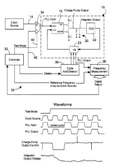
Refererence will now be made to the block-level diagram in Figures 3 and 4,
which illustrate a test circuit and a flow diagram respectively, according to
one
embodiment of the present invention. The test circuit, generally designated by
reference numeral 30, includes a control circuit or controller 32, a
multiplexer 34, a
cycle addition/deletion circuit 36, illustrated in Figure 16, and a frequency
measurement circuit 38, illustrated in Figure 15. Multiplexer 34 is controlled
by a
Test Mode signal 40 provided by controller 32 and receives the clock input 14
and a
feedback clock signal 42 output by the cycle addition/deletion circuit 36. A
nominal
frequency stimulus (clock or data) is normally applied to the input of the PLL
by the
controller applying a low level signal to the multiplexer (step 46) in Figure
4.
Self-test can typically begin only when the PLL output frequency is locked to
the input frequency. Many PLLs have a phase lock output which indicates when
the
output phase is locked to the input phase. This 'Lock' signal can be used in
test
mode to initiate self-test. Alternatively, a frequency 'valid' detector (not
shown) can
be incorporated into controller 32 to generate an output logic signal whenever
the
output frequency of the PLL is within a chosen bandwidth around the input
frequency. The detector can reduce test time by initiating self-test before
the PLL
has locked to the phase or frequency of the input signal. Thus, under the
control of
controller 32, the first steps in the self-test process is to either measure
the VCO
CA 02220622 1997-11-03
-7-
frequency or observe the PLL'Lock' signal (step 48) and determine whether the
frequency is within a predetermined range or the PLL has output a 'Lock'
signal
(step 50).
When the PLL output frequency is valid, the controller outputs a logic high
Test Mode signal to the control input of multiplexer 34 to select the feedback
clock
input 16 instead of the input clock 14 (step 52). At this point, the feedback
clock is
the same as the clock fed back into the phase comparator 12 within the PLL,
and
therefore the phase error becomes approximately zero. The output of the phase
comparator becomes high impedance, and the output voltage of the charge pump
integrator 20 becomes approximately constant, as shown in Figure 3. Typically,
there will be some phase error and the integrator output voltage will slowly
increase
or decrease. Immediately after entering this mode, the output clock frequency
is
measured over a time interval T and the result is denoted fo (step 54). The
frequency is then immediately measured again (step 56) over another time
interval
T, and the result is denoted f,. The value of f,-fo is representative of the
magnitude
of the frequency drift due to various sources, including the phase error
introduced by
the test circuitry. It is also possible to measure fo while the PLL is in the
Lock
state; however, the value of f,-fo will be one-half of the value compared to
the
method just described.
Next, under the control of controller 32, cycle addition/deletion circuit 36
eliminates a single cycle (step 58) from the feedback clock and then there is
a pause
(step 60) for a few cycles to permit transients to settle. Immediately after
the cycle
is eliminated, the output clock frequency is again measured over a time
interval T
and the result is denoted f2 (step 62). The value of (f2 f,)-(f,-fo) is
representative of
the change in frequency due to the single pulse deletion and can be shown to
be
proportional to the loop GBW of the PLL. This value is determined (step 64)
and
compared to a predetermined value (step 66), which results in a 'Pass'
or'Fail'
condition. The controller then re-enables the normal input via the multiplexer
(step 68).
In some cases, the frequency change caused by a single cycle deletion is too
small to accurately measure in the chosen time interval T. In these cases, two
or
more cycles can be deleted, and the result will be proportionally larger. In
other
cases, deleting even a single cycle causes excessive frequency shift. In these
cases, a portion of a cycle can be deleted - for example, a quarter or an
eighth of
CA 02220622 1997-11-03
_g_
the cycle can be precisely deleted using synchronous logic. Alternatively, a
combinational logic gate delay can be used to delete a constant interval of
time from
a cycle, and the delay of the logic gate can be measured using other means.
Another, more direct method for introducing phase shift is to use
synchronous logic to continuously delay the feedback signal by 90°,
45°, 22.5° or
some other angle equal to 360°/2", where n is some positive integer.
However, this
method is only practical when the divide ratio (N in Figure 1) is large enough
to
permit digital generation of the necessary delay, and when the loop GBW is not
so
high that the integrator output voltage goes into saturation before the
frequency is
measured. In general, deleting one cycle causes a 180° (or 360°,
depending on
phase comparator design) phase step, which decreases the output frequency the
same amount as a 1 ° phase error for 180 (or 360) cycles.
In summary, the method described above first connects the loop feedback
signal into both inputs of the phase comparator so that its output becomes
independent of the VCO output and hence the PLL is tested in open-loop mode.
Next, a phase error is introduced for one or more clock cycles, and the
resulting
change in output frequency is proportional to the loop GBW.
Measurement of Loop GBW for Exor-type PLL
Reference will now be made to the block-level diagram of Figure 5, which
illustrates a test circuit 80 for measuring Loop GBW for an Exor-type PLL
illustrated
in Figure 2, and to Figure 6, which is a flow chart for measuring the GBW for
an
Exor-type PLL according to a preferred embodiment of the invention. As with
test
circuit 30, test circuit 80 includes a controller 32, a multiplexer 34, a
cycle
addition/deletion circuit 36, and a frequency measurement circuit 38.
For this type of PLL, self-test should be initiated only after the 'Lock'
condition
is detected. When the Lock condition is detected (step 82), controller 32
enables the
feedback with a 90° phase shift by applying a logic high (step 84) to
the control input
of multiplexer 34 to select the feedback clock instead of the input clock. The
controller then waits (step 85) a sufficient number of cycles for the output
frequency
to settle. After the pause, the controller counts VCO output cycles for 5J
feedback
cycles and then stores the number of cycles counted as count1 (step 86).
Next, the controller starts a new count (step 88) and changes the feedback
phase shift to 0° for J cycles (step 90). At the end of the J cycles,
the controller
CA 02220622 1997-11-03
_g_
again pauses (step 92) for another predetermined number of cycles, such as 4J
cycles, and then stops counting and stores the final count as count2 (step
94). J is
an integer whose value may be 32, for example, (J is shown as 6 in Figure 5 to
simplify the illustration). The feedback clock made is the same as (or
inverted
relative to) the clock fed back into the phase comparator within the PLL, and
therefore the phase difference becomes approximately zero (180°).
However, since
the normal phase difference for the Exor-type PLL is typically 90° in
the center of the
PLL frequency range, the output of the phase comparator becomes a continuous
logic low (or logic high), as shown in Figure 5, and the low pass filter
output voltage
begins to fall (or rise), which causes the output frequency to decrease (or
increase).
The normal input is re-enabled via the multiplexer 34 and the Loop GBW product
is
determined (step 96). It can be shown that the GBW product is proportional to
the
difference between the two counts, count1 and count2, multiplied by the ratio
of J/N.
For a PLL with a low value for loop GBW, J can be a large integer to ensure
that sufficient frequency deviation occurs. For a PLL with a high value for
loop GBW,
the value of J should not be so large as to allow time for the low pass filter
(LPF)
output to reach a constant value. The resolution of the output is equal to
~4~, so
small values of J should be also be avoided. An alternative way to accommodate
high values of loop GBW and a sufficiently large value for J is to feedback a
clock
whose phase has been shifted by some value between 0° and 90°.
For example,
45° is an easily generated value in some cases. Alternatively, a
constant delay can
be used to provide a different phase shift, such as that provided by a
combinational
logic gate whose delay can be measured using other means.
Measurement of Lock Range
Reference will now be made to the Flow Diagram in Figure 7 which illustrates
a procedure for measuring the frequency lock range of a PLL containing a
charge-pump phase comparator. The circuitry described earlier with reference
to
Figure 3 for measuring loop GBW can be used for lock range measurement, with
modifications to controller 32 only to implement the different sequence.
The procedure can begin immediately after a value of DFo (f2-f,) - (f,-fo) is
determined in the Loop-GBW procedure illustrated in Figure 4. Then, another
cycle
is deleted (or added) (step 98) and the VCO frequency is measured again (step
100), as f3. Next, the value DF=(f3 fZ) - (f,-fo) is determined and compared
to DFo
CA 02220622 1997-11-03
-10-
(steps 102 and 104, respectively) If the value of DF is within some range of
DF°,
for example within a factor of two, then the GBW is decreasing (or increasing)
sufficiently linearly. Cycles are continually deleted (or added) (loop 106)
until the
value of DF is no longer within range of DF°, at which time the GBW is
assumed to
be nearing saturation or a very non-linear region of operation, and hence the
lock
range limit has been exceeded. At this point the procedure is terminated and
the
normal input is enabled (step 108). The last frequency measured in the linear
region
is the lower (or upper) limit of the frequency lock range (step 110).
A significant advantage of this procedure is that only a constant frequency or
data rate needs to be applied to the PLL by external test equipment, which
greatly
simplifies the test equipment and test program, reducing test development time
and
cost of testing.
Measurement of Lock Range for Exor-fype PLL
Figure 8 is a flow chart which illustrates a procedure for measuring the
frequency lock range of a PLL containing an Exor gate phase comparator. The
circuitry shown in Figure 4 described earlier for measuring loop GBW can be
used
for lock range measurement, with modifications to only controller 32 to
implement the
different sequence.
As in the GBW measurement, a nominal frequency clock or data is applied to
the PLL input, and after phase lock is achieved, the 90° phase shifted
output is
feedback into the PLL via multiplexer 34, so that the duty cycle at the output
of the
Exor gate internal to the PLL becomes 50%. A short settling time may be
required
for the VCO output frequency to become stable, and proportional to the 50%
duty-cycle.
Next, for C cycles out of every M cycles of the feedback signal (loop 112),
the
phase shift is changed to 0° (or 180°) which causes the PLL
output frequency to
decrease (or increase). C and M are integers, and C is increased from 0 to M-
1,
where M is, for example, 8. The output of the Exor gate will then have an
average
duty cycle of 50%-100%xC/M (or 50%+100xC/M).
The frequency f~ is measured (step 114) each time C is increased. The value
of DF=f° -f~, is determined (step 116) and compared (step 118) to
DF,=f,-f°. If the
value of DF is within some range to DF,, for example within a factor or two,
then the
GBW is decreasing (or increasing) sufficiently linearly. C is increased (step
120)
CA 02220622 1997-11-03
-11-
until the value of DF is no longer within range of DF,, at which time the GBW
is
assumed to be nearing saturation or a very non-linear region of operation, and
hence
the lock range limit has been exceeded. At this point the procedure is
terminated
and the normal input is enabled (step 122). The last frequency measured in the
linear region is the lower (or upper) limit of the frequency lock range (step
124), i.e.
the lock range is f~,.
Measurement of Parameters which affecf Bit Error Rate
Using a circuit such as that shown in Figure 9, which is similar to circuitry
described for testing loop GBW of an exor-type PLL (Figure 5), it is possible
to
adjust the phase error for selected bits in the data stream. By increasing the
phase
error used to detect bits in a noise-free data stream until bit errors are
induced, it is
possible to determine how much inherent phase error and noise is present in
the
detection circuitry and thus to estimate the BER that would occur without any
induced phase error. For a noise-free data stream, the BER is typically too
small to
measure economically, so the method of the present invention can save
considerable time and expense.
As was demonstrated for testing loop GBW, deleting (or adding) one or more
sequential clock cycles has the same effect as a step increase in phase error
(see
the waveforms of Figure 6), and causes the PLL to respond in a way which
reduces
the phase error, i.e. the integrator or LPF output decreases (or increases) at
a rate
determined by the loop GBW. As soon as the clock cycles are no longer deleted,
the
integrator or LPF output increases (or decreases) to its original value, but
at a slower
rate. This rate was measured in the loop GBW test for the exor-type PLL. The
clock
cycle immediately following the Jt" clock pulse deleted will have a
predictable phase
error, and this phase error will increase for each subsequent clock cycle as
long as
clock cycles are being deleted. Using this principle, precise increments in
phase
error can be introduced. An example process which uses this principle will now
be
described with reference to Figures 9, 10 and 14.
Before initiating the process, an input data stream 130 is applied as stimulus
to the PLL, which is in a closed-loop mode. The input data stream may be a
pseudo
random bit stream (PRBS), alternating 1's and 0's, or a clock. Bit errors are
detected
by conventional means. For example, Figure 14 shows a P-bit (e.g. P=8) linear
feedback shift register (LFSR) serially loaded with the received data, which
is
CA 02220622 1997-11-03
-12-
presumed to be temporarily error-free, and then data is fed back within the
LFSR
which causes a correctly initiated PRBS to be continually generated for
comparison
with the received PRBS. Any comparisons which reveal a difference are counted
by
a BER counter. Typically, P is 8, 12, or 16, but, if the data is simple
alternating 1's
and 0's, then P is 1.
As indicated in more detail below, the input data stream is interrupted so as
to delete J cycles. This causes the phase error of the PLL output to increase
relative
to the data stream. The values of J, a BER counter, and x, a subscript for
each BER
count, are initialized (step 132) to zero. J is the number of sequential
cycles which
are deleted. A process cycle counter, K, is set to 1. Controller 32 then
executes
loop 134 to confirm that the PLL frequency is in range or that the 'Lock'
signal is
present.
When the data stream is a clock or alternating 1's and 0's (which is a half
speed clock), the data stream may be used to clock the circuit which deletes
cycles.
When the data stream is a PRBS, the PLL output clock may be used to clock the
circuit which deletes (or adds) cycles; in this case, as phase error
increases, a non-
integer number of cycles (bits) will be deleted.
With particular reference to Figure 10, the process involves the following
sequence of steps:
First, J data stream cycles are deleted (step 136), and, if there is a bit
error at
the end of the Jt" cycle (step 138), the BER counter is incremented (step
140). This
step is followed by a pause (step 142) of approximately 4J clock cycles,
during which
no cycle deletion occurs and phase lock is regained. If the number of
sequences K
has not reached its maximum preset value (step 144), Km~ which may be 1,000
for
example, loop 146, comprising steps 136, 138 and 142, is repeated.
When K reaches Km~, BERo is checked to determine if it exceeds a
predetermined value (step 148), such as 1. If it does not, J is incremented
(step
150), K is reset to 1 (step 152), and BERX is set to zero (step 154). A loop
156,
comprising steps 136, 138, 142, 144 and 148, is repeated.
If at step 148, BERo is found to exceed the predetermined value, the value of
the BER counter output is recorded (step 158) as BERX, checked to determine
whether it has reached a maximum preset BERm~ (step 159) and, if it has not, x
is
incremented at 160, and then loop 156 is repeated. If BERX has reached its
maximum, the process is terminated at 162 where the BER for J=0 is determined.
CA 02220622 1997-11-03
-13-
The BER can be estimated by appropriately extrapolating the values of BER
(BERo,
BER,, ...) versus J (Jo, J,, ...) to the point where J=0 using any of various
mathematical relationships that have been published relating phase error to
BER.
Alternatively, the BER values can be compared to BER values measured in
several
manufactured units of the IC whose true BER for J=0 and whose BER for other
values of J is known. For example, if the in-system BER for one unit of the IC
is
measured as BERa, and the BER for another unit is BERb, and then the values of
BER versus J for each unit are measured, the relationship can then be
calculated
between in-system BER and the extrapolated value of BER versus J.
Many variations on this method are possible. For example, less than a full
pulse can be deleted each time, as previously described for loop GBW
measurement. This allows smaller increments in phase error, but requires N>2
to
ensure that sufficient clock edges are available to create a synchronous phase
delay.
Further, a phase error, C clock cycles after pulse deletion (or addition)
ceases, can be used - this phase error will decrease more gradually than when
cycles were being deleted, and thus allow smaller phase steps. C is increased
each
time that loop 156 is repeated, instead of increasing J.
CA 02220622 1997-11-03
-14-
Measurement of Jitter and Phase Error
Another important parameter of a PLL is the output clock phase fitter relative
to an ideal clock. In the method described herein, fitter is measured relative
to the
input clock or data, either of which is assumed to be fitter free.
In accordance with the method of the present invention, Jitter is measured by
introducing a progressively increasing delay into the PLL input while
monitoring the
PLL output for incorrect bits and determining (a) the value of the delay at
which
detected bits cease to be continuously correct and (b) the value of the delay
at which
a predetermined number of detected bits are incorrect. The difference between
the
two values is equal to the peak-to-peak Jitter. Figure 12 illustrates a
circuit 170
which can be used to measure Jitter and Figure 13 is a flow diagram
illustrating a
procedure for measuring Jitter.
With reference to Figure 12, circuit 170 includes controller 32, a delay
mechanism 171, a latch (or D-type flip-flop) 172, a BER counter 174, a
frequency
counter 176 and a multiplexer 178. Delay mechanism 171 may be in the form of a
series non-inverting logic gates such as is shown at 216 in Figure 13. The
normal
input 180 to the PLL 10 is a reference clock, a PRBS or alternating 1's and
0's which
is input to the controller and to the input of delay mechanism 171. The
outputs of
counters 174 and 176 are fed back to the controller, as shown. The output 182
of
the PLL is also fed back to the low input of multiplexer 178, the output of
which is
applied to the input of a tapped delay mechanism 183 the output of which is
input to
the clock input of latch 172. Tapped delay mechanism 183, illustrated in
Figure 13
and described later., is controlled by controller 32. Delay mechanism 171
introduces
a constant delay into the PLL output and a delayed output data stream 184 is
delivered to the input of the PLL and to the data input of latch 172. The
output of the
latch is connected to BER counter 174.
Referring to Figure 11, initially, a nominal frequency stimulus is applied to
the
PLL (step 186) and the PLL is permitted to achieve a 'lock' condition (loop
188).
Concurrently, a number of variables are initialized as shown at 190 and the
delayed
output data stream 184 is connected to the data input of latch 172. A delay is
then
introduced into the data stream at 192 and then the PLL is allowed to free
run. The
delay may be achieved by seeding an N-bit LFSR (not shown) with incoming data.
BER counter 174 then counts the number of bit errors, B, in K consecutive
cycles of
the PLL output (step 194) and outputs the results to controller 32. The
controller
CA 02220622 1997-11-03
-15-
then determines whether B is less than a predetermined value, Low, (step 196)
and,
if so, increases the delay by a value, delta, (step 198) and then repeats
steps 194
and 196. If B is greater than Low, controller 32 performs a reference delay
measurement to obtain D~oW (step 200). The controller then determines at 202
whether B is less than another predetermined value, High, and, if so,
increases the
delay by a value, delta, at step 198 and then repeats steps 194 and 196. If B
exceeds the value High, the controller performs a reference delay measurement
to
obtain DHigh at step 204. With the values of D~aW and DH;9h, it is possible to
determine
Jitter at 206 by determining the difference between the two values. The Jitter
can be
compared at step 208 against some predetermined value to determine whether the
circuit passes or fails.
The sequence, just described, is a linear search for the time range limits of
the fitter. Other searches, such as a binary search, could be used. The delay
difference obtained can be measured using any of several schemes, for example,
by
inserting the delay into an oscillating loop and measuring the resulting
increase in
oscillation period: Figure 12 shows this circuitry in dashed outline as an
example.
When the stimulus bit stream is alternating 1's and 0's, DHigh will be 100% of
the
number of bits counted. When the stimulus bit stream is a PRBS, DHigh will be
some
predictable number less than 100%, since many adjacent bits in the PRBS will
be
identical and hence a one-bit delay will not appear to cause an error. The
value of
DHigh for a particular PRBS is equal to the number of bit errors that would
result if the
PRBS were compared to itself delayed by one bit interval.
To insert delay into an oscillating loop, a circuit such as that shown using
dashed lines in Figure 12 is used. An offset delay 171 is provided to allow
fitter
measurement in the presence of zero or negative inherent phase error.
The definition of "continuous", as used in the preceding description can be
adjusted by the circuit designer. For example, continuous could mean a
duration of
1024 bits. The duration should be an integer multiple of the PRBS length.
Lower
numbers allow faster tests but may not detect a low frequency fitter.
Another measure of fitter is the time range in which X% of the fitter occurs.
For example, if X=80, then the fitter delay range would be from 10% to 90%,
corresponding to a range from 102 bits in error to 918 bits in error out of
1024 bits.
To accomplish this measurement, each time the delay is increased, the number
of
errored bits is compared to a programmable limit or shifted off-chip.
CA 02220622 1997-11-03
-16-
It is preferable to measure fitter for a pseudo-random bit sequence (PRBS)
since it is more representative of typical data. The data stream is generated
using
an LFSR with P bits, on-chip or off-chip, filtered by a transmitter filter and
a receiver
filter and then sampled using latch 172 (or D-type flip-flop) which is clocked
by the
PLL output. The output of the latch is compared against the correct value to
check
for bit errors. The correct value can be obtained typically using a second P-
bit LFSR
which is the same as the transmit LFSR but is bit-synchronized to the received
data
stream. As previously mentioned, bit synchronizing is accomplished by loading
in
any series of P bits which are error free.
Figure 13 illustrates an example tapped delay line 210 which includes a
binary counter 212, a multiplexer 214 and a series of taps 216. The input
signal is
applied to the first tap and the desired tap count is applied to the counter
212. The
output of the multiplexer is a signal having the desired delay.
Figure 14 illustrates an example of a BER counter which includes a linear
feedback shift register 218, a binary counter 220, an output register 222 and
combinational logic.
Figure 15 illustrates the frequency measurement circuit 38 for measuring
frequency. The circuit includes a 2R divider 224, which receives a known
frequency,
an AND gate 226 which receives the frequency to be measured and the output of
the
divider, a binary counter 228 which receives the output of the AND gate and of
the
divider, and an output register 230 which receives the output of the counter
and of
the divider and outputs the new frequency of the PLL.
Figure 16 illustrates a cycle deletion circuit 36 which can be used for cycle
elimination. The circuit includes two D-type latches 232 and 234 and
combinational
logic, including a pair of AND gates 236 and 238. The input clock is applied
to AND
gate 238 which produces a new output clock signal. When a 'delete' input is
applied
to latch 232, the circuit substitutes a logic low for a logic high in the
input clock
signal.
Figure 17 illustrates a circuit 240 which is adapted to perform either cycle
deletion or cycle addition. The circuit includes three D-type latches 242, 244
and
246 and combinational logic 248. It is believed that the operation of the
circuit will be
apparent to a person skilled in this art and, accordingly, the operation is
not be
described herein.
CA 02220622 1997-11-03
-17-
It will be seen that the foregoing has described circuitry and processes for
measuring various parameters of PLLs, including loop GBW, lock range, BER,
Jitter,
and phase offset, without connecting to the internal components of the PLL.
While
individual circuits have been described and illustrate for determining these
parameters, it will be understood that the individual circuits can and
normally would
be combined into a single BIST circuit capable of performing all of the
required
measurements.
It will also be understood that the present invention is not limited to the
specific circuits described and illustrated and that various other
modifications and
alterations may be made thereto by persons skilled in the art without
departing from
the spirit of the invention defined in the appended claims.