Note: Descriptions are shown in the official language in which they were submitted.
CA 02220781 1997-11-12
MILLIMETER WAVE TRANSCEIVER FOR POINT-TO-
MULTIPOINT COMMUNICATIONS SYSTEM
Field of the Invention
The invention relates to a low power, directional
millimeter wave transceiver for use in a point-to-multipoint
two-way communication system.
Backqround
Millimeter wave transceivers for use in GHz frequency
bands are known in association with a variety of radar
applications such as those disclosed in U.S. patent Nos.
4,893,126, 5,201,065, 5,512,901 and 5,493,303.
Millimeter wave transceivers have, more recently, been
disclosed for local reception and transmission of
television/radio signals and digital data in point-to-
multipoint communication systems. For example, U.S. patent
No. 4,747,160 discloses a low power multifunction cellular
television system in which a subscriber receiver locks to a
master oscillator located at a cell node transmitter.
However, the transceiver taught by this patent is costly,
complex and is not subject to compact construction because the
space diversity provided therein between the reception and
transmission antennas requires that those antennas be spaced a
longitudinal distance from each other. Furthermore, the
transceiver disclosed therein provides limited frequency
CA 02220781 1997-11-12
diversity, through polarization of the reception and
transmission functions only, and does not disclose any
frequency planning for m;n;m;zing interference or cross-talk
between distinct types of reception signals. Also, the
subscriber receiver taught by this patent utilizes a manually
tuned oscillator and the method of transmitting data is not
disclosed.
Consequently, it is desirable to provide for a low cost,
integrated-circuit millimeter wave transceiver utilizing
frequency planning and having a compact construction including
planar reception and transmission antennas and programmable
computer-controlled local oscillators.
Summarv of the Invention
In accordance with the invention there is provided a
directional millimeter wave transceiver for reception and
transmission of signals comprising digital data and/or
broadcast television/radio signals in a point-to-multipoint
communication system. A receiving antenna directionally
receives millimeter wave signals having a first predetermined
polarity and a transmitting antenna coplanar therewith
directionally transmits millimeter wave signals having a
second predetermined polarity which is orthogonal to the first
polarity. Digital data signals are received by the receiving
antenna within a first predetermined frequency band, digital
data is transmitted by the transmitting antenna within a
second predetermined frequency band and broadcast
television/radio signals are received by the receiving antenna
within a third predetermined frequency band whereby the second
frequency band is between the first and third frequency bands.
CA 02220781 1997-11-12
Radio frequency circuitry is provided to convert the
millimeter wave signals to and from intermediary frequency
signals whereby the radio frequency circuitry receives the
broadcast television/radio and digital data signals from the
receiving antenna, converts the received signals to
intermediary frequency signals and separately outputs the
radio frequency television/radio and data signals. In
addition, the radio frequency circuitry receives intermediary
frequency data signals, converts the intermediary frequency
data signals to millimeter wave data signals and outputs the
millimeter wave data signals to the transmitting antenna.
Coding/decoding circuitry is provided for
modulating/demodulating and coding/decoding the intermediary
data signals to condition the intermediary signals for output
from the transceiver to a local data network and for input to
the radio frequency circuitry.
The receiving and transmitting antennas 80, 90 are
comprised of separate parabolic antennas. The radio frequency
circuitry is comprised in a single circuit card 110 and the
coding/decoding circuitry is also comprised in a single
circuit card 240. The antennas and circuit cards are
assembled together within an external housing 275.
The radio frequency circuitry preferably comprises a high
frequency oscillator circuit comprising a low frequency
synthesizer and multiplication circuitry for multiplying the
low frequency synthesizer to a selected millimeter wave
frequency. The radio frequency circuitry also includes
mixers, an input of which is the output of the high frequency
oscillator circuit, and phase locked loop circuitry. The
coding/decoding circuitry preferably comprises microprocessor
CA 02220781 1997-11-12
means for permitting local control of the operating frequency
of the transceiver by providing control to the high frequency
oscillator circuit and the phase locked loop circuitry. The
coding/decoding circuitry also preferably comprises a
reference signal generator for input to the high frequency
oscillator circuit and the phase locked loop circuitry, and DC
power supply circuitry for use by the radio frequency
circuitry and the coding/decoding circuitry.
Brief Description of the Drawinqs
Figure 1 is a representational layout of a point-to-multipoint
two-way communication system utilizing a transceiver according
to the invention at the subscriber end thereof;
Figure 2 is a representational layout of a typical subscriber
end in the communication system shown in Figure 1;
Figure 3 is a general block diagram representation of the
components of the transceiver according to the invention;
Figure 4 is a graphical representation of the frequency plan
of the transceiver according to the invention;
In Figure 5, Figs. 5(A) and 5(B) are block diagram schematic
representations of the preferred polarized parabolic reflector
receiving and transmitting antennas, resp., and Figs. 5(C) and
5(D) are block diagram schematic representations of
alternative polarized, planar, printed patch receiving and
transmitting antenna arrays, resp.;
Figure 6 is a block diagram of the radio frequency circuitry
CA 02220781 1997-11-12
of the preferred embodiment of the transceiver according to
the invention;
Figure 7 is a block diagram of the coding/decoding circuitry
of the preferred embodiment of the transceiver according to
the invention;
Figure 8 is a diagrammatic break-out assembly drawing showing
the assembly of the subassembly components of the preferred
embodiment of the transceiver according to the invention; and,
Figure 9 is a perspective view of the assembled transceiver
according to the preferred embodiment of the invention.
Detailed DescriPtion of a Preferred Embodiment
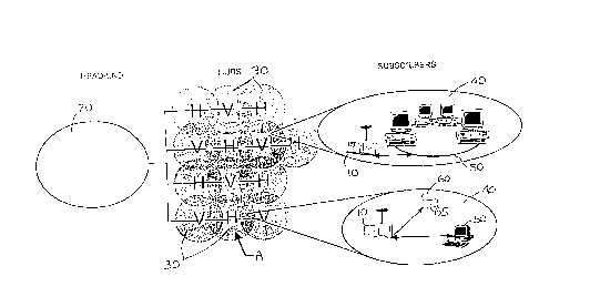
Referring to Figure 1, the directional transceiver 10 of
the invention is used at the subscriber end of a point-to-
multipoint communications system as illustrated, the
commlln;cations system comprising a head-end 20, a plurality of
alternately polarized hub stations 30 and a plurality of
subscribers 40 within each area covered by a hub station 30.
The head-end 20 of the communications system includes the
usual broadcast equipment plus head-end-to-hub transmission
equipment for transmitting both digital data (representing the
data link function of the system) and analog television/radio
signals (representing the direct broadcast, "DB", function of
the system) to the hub stations 30. At the head-end the
television/radio broadcast signals are collected from the
various sources of those signals and data signals are
collected from various digital data sources such as the
Internet.
CA 02220781 1997-11-12
Preferably, as illustrated, the communications services
provided include various data links, such as to the Internet
and the many services providing access to various databases
world-wide, and a broad scope of television/radio broadcast
channels. Thus, business subscribers utilizing the data links
and home subscribers using either or both of the data links
and television/radio channels may benefit from the
com~lnications system.
The hub stations 30 are omni-directional transceivers
which transmit and receive the communications signals at
approximately 28 GHz. By reason of regulatory safety
standards which govern the maximum permissible power levels
for millimeter wave transmissions, the transmission/reception
radii covered by a hub station transceiver 30 or subscribe
transceiver 10 is about 5 Km. The maximum power output
transmitted by the subscriber transceiver 10 is lOmW. To
obtain effective coverage over the area of a city (marked by
"A" in Figure 1) a plurality of hub transceivers 30 are
positioned so that their areas of coverage overlap with the
areas of adjacent transceivers 30 and the polarities of the
transmissions/receptions by adjacent hub transceivers 30 are
orthogonal as illustrated. Because the overlapping signals in
any one area are orthogonal a subscriber transceiver 10 in
such area is selected to have polarities matching those of the
hub transceiver 30 providing the strongest signals at such
location so as to block out the weaker orthogonal signals of
the overlapping hub transceiver 30.
At the subscriber end 40 the local transceiver 10
receives digital data signals and analog television/radio
signals on the millimeter wave carrier frequency transmitted
CA 02220781 1997-11-12
by the hub transceiver 30 to which it is directionally
coupled. The transceiver 10 transforms these signals back
into their digital data and analog television/radio components
for output from the transceiver 10 to a local data network 50
(which is preferably a Tl interface/switch or an Ethernet
interface) and television set-top receiver unit 60,
respectively, as illustrated by Figure 2. Two-way data
communications are provided by the transceiver 10 which also
receives digital data signals from the local data network 50,
transforms them into millimeter wave signals and transmits
those signals to the hub transceiver 30 associated with the
local transceiver 10.
Referring to Figure 3 a general block diagram
representation of the components of the transceiver 10 is
provided. Directional receiving antenna 80 and transmitting
antenna 90 are orthogonally polarized so as to provide
electrical isolation between the two antennas. In the
embodiment shown by Figure 3 the receiving antenna 80 is
vertically polarized whereas the transmitting antenna 90 is
horizontally polarized. A transceiver 10 configured
accordingly would, therefore, be located in an area covered by
a hub transceiver 30 having a vertically polarized
transmitting antenna and horizontally polarized receiving
antenna. Each of the antennas 80, 90 are highly directional
and must be positioned in line with their associated hub
transceiver 30 (or a repeater positioned therebetween for
directional modification/amplification purposes). This
directionality of the antennas 80, 90 assists in the
electrical isolation of the antennas 80, 90 and of individual
subscriber transceivers 10 located in the subscriber end 40 of
the communications system.
CA 02220781 1997-11-12
The receiving antenna 80 and the transmitting antenna 90
are parabolic reflector antennas with LEXON (a trademark)
windows as illustrated in Figures 5(a) and 5(b), the receiving
antenna shown in Figure 5(a) being an antenna with a linearly
vertically polarized feed element and the transmitting antenna
shown in Figure 5(b) having a linearly horizontally polarized
feed element. Optionally, the antennas could instead be
planar, printed patch antenna arrays as illustrated in Figures
S(C) and 5(D) wherein Figure 5(C) shows a receiving array of
linearly vertically polarized patch antenna elements and
Figure 5(D) shows a transmitting array of linearly
horizontally polarized patch antenna elements. The antennas
provide highly focused beams whereby very directional
reception and transmission is obtained while simultaneously
rejecting undesired signals outside of the focused beams. The
preferred parabolic reflector antennas are produced by
InfoMagnetics Corporation and identified as Part No. 27.85R-
30. They allow for a high degree of electrical isolation
between the receiving and transmitting antennas, typically in
the order of 20 - 30 dB at 28GHz. This isolation allows the
transmit signal, which "leaks" into the receive stream, to be
suppressed sufficiently so as not to cause distortion of the
signals being received and, thereby, allows for simultaneous
reception and transmission by the antennas 80,90.
Additional electrical isolation between the different
types of communication signals is provided by the frequency
plan employed by the transceiver 10 as illustrated in Figure
4. As shown, the operating frequency band for the
transmission and reception of signals within the
commlln;cations system is about 1 GHz (marked by the dotted
lines in Figure 4) and suitable guard bands "C" and "D" at the
CA 02220781 1997-11-12
upper and lower limits of the operating band are provided to
avoid "leakage" or cross-talk from outside the allocated
operating frequency band. Within the operating band a
frequency band 140 of about 200 MHz is reserved for digital
data signals and a band 160 of 500 MHz is reserved for analog
television/radio signals, with a suitable guard band "E" of
240 MHz provided between the data signal and the
television/radio signal bands. Within the digital data signal
band 140 a further two distinct frequency bands 142, 144,
separated by a guard band "F", are allocated. The first data
signal band 142 is reserved for received data signals and the
second data signal band 144 is reserved for data signals to be
transmitted by the transceiver 10 such that the frequency band
142 allocated for the reception of digital data is separated
from the frequency band 160 allocated for the reception of
television/radio signals by the band 144 allocated for
transmission of data signals. The reception functions for
digital data and analog signals are thereby electrically
isolated by the frequency bandwidth allocated for transmission
of digital data which is itself electrically isolated from
both reception functions due to the orthogonal polarities as
between the reception and transmission functions. These
isolating functions allow for the simultaneous reception and
transmission of both digital data signals and analog
television/radio signals without need to separate the transmit
and receive signals at the RF input frequency.
The radio frequency (RF) circuitry 110 shown by Figure 6
converts the millimeter wave signals (i.e. the RF within the
operating frequency band around 28 GHz) to and from
intermediary frequency (IF) signals using synthesized local
oscillators. The RF circuitry 110 comprises a receive portion
CA 02220781 1997-11-12
150, a transmit portion 152 and a high frequency local
oscillator portion 154 providing input to microwave integrated
circuit mixers 156, 158 of the receive and transmit portions
150, 152, respectively. The high frequency local oscillator
154 uses a low frequency synthesizer which is multiplied to a
high frequency band around 26.8 Ghz. The low frequency
generated by the phase locked loop 160 is amplified by two
amplifiers 198. The required harmonic of this signal is
extracted by a comb generator 208. A base band filter 206
eliminates unwanted signals and the resultant Ka-band signal
is amplified using two monolithic power amplifiers 204 and is
divided between the receive portion 150 and the transmit
portion 152 using a power divider 202.
The receive portion 150 receives signals from antenna 80,
filters the required signals with filter 180, amplifies the
resultant signal with two monolithic low noise amplifiers 182
and then down converts the signal to intermediary frequencies
~490 MHz - 1,450 MHz) using a microwave integrated mixer
circuit 156 and the Ka-band signal provided by the high
frequency local oscillator portion 154. The mixer 156
includes an image notch filter for image suppression in the
down conversion. Intermediary frequencies above 1,450 MHz are
filtered out by a surface mounted IF band pass filter 186 and
amplified 188. A surface mounted power "divider" 190 divides
the signal into two paths.
The receive portion 150 provides two output signals, one
being an IF television/radio signal (950-1450 MHZ) which is
typically (but not necessarily) an analog signal and is fed to
a set-top television receiver 60 and the other being a 70MHz
IF output comprising digital data which is fed to the
CA 02220781 1997-11-12
coding/decoding circuitry provided by a power supply/coder-
decoder circuit card 240. The transmit portion 152 receives
modulated, coded IF digital data signals from the
coding/decoding circuitry 240 and converts the IF signals to
RF (millimeter wave) data signals for output to the transmit
antenna 90. Local control at the transceiver 10 is provided
to the high frequency local oscillator 154 and the phase-
locked loop circuits 160, 162 and 164 of the RF circuitry 110
by a microprocessor 170 having frequency settings for user
selection to provide such local control. Particulars of the
individual block elements of Figure 6 are provided below under
Table 6.1
CA 02220781 1997-11-12
T~bk 6.1-Rad;OFI~. r~ C-~ ~ CL . OfF;gU~ 6
Referenoe No. Name SD~fic-~ - tDea~ Vendor (if
~llDliC '~)
156 Mixer* Do... ~ t~_lb the incoming Ka-band signals
to~ ~ signals
158 Mixer* U~o.. ~_ b the int~ l;at~ signals to Ka-band
160 Low Band Phase Serial input phase-locked-loop ~ ' ~ with Fujitsu and
Z-comm
Locked Loop** a .~.~ from 10 MHz crystal os~ ll ~ -
162, Phase Locked Loop** Serial input phase-locked-loop a~llthc~er Fujitsu
164
180 RF Band Pass Filter* Eliminates r,., - outside the band of interest
182 2-Stage Low Noise Low noise ~ r~ with a noise figure of 2.8 dB Alpha
Amplifier*** Tr' ~~
184 Image Notch Filter* A notch filter to suppress image L~, ~ by 15 dB
186 IF Low Pass Filterr** Low pass filter with cut offfi~ue"~ at the edge LarkF~
of the i. ~ fi~ue~l~ band
188 IF Amplifier ** Amplifies the ~ ~ - ' ~ signals to match input Mini
Circuits
level ~u,,~ to TV set top box
190 Power Divider** Divides the ~ ~t ~ - y signals into two paths Mini
Circuits
192 T ~ from T ~ with lumped elements
50 to 75 o}uns**
194 Mixer** Do.... ,~ll~el~ the ~ ~ ~ signals to 70 MH~ Mini
Circuits
196 70MHz Surface Band pass filter with oenter fi-~t .~ at 70 MHz Sawtek
Acoustic Wave Filter** to provide istolation between adjaoent cham els
198 ~ FET ~ , 'ifirr used to amplify low phase-locked- Celeritek
loop output
200, Voltage Controlled Oscillator in low r,. tt ~ phase-locked-loop Z-Comm
218 o~ill- t~t~
202 Power Divider* In-phaae design, insertion loss is 3 dB +/- 1 dB
12
CA 02220781 1997-11-12
T~ble 6.1~ d)
Referenoe No. Name S~ific ~finn~De~ io~ Vendor (if
e)
204 Two Stage Dnver ~ , ' to boost up the Ka~and local Alpha
Amplifier*** o~ill signal
206 Bandpass Filter* Filters the local os~ signal
208 Comb Gi~ Extracts the 13th 1 1 - of the low band Herotek
phase-locked signal
210 Power Aml~liliel~t~Amplifies the signal to be ll_ ~1 Alpha
;PS
212 Low Noise Amplifies the signal to be i ' Alpha
~0~l- -- ' . i~s
Alllpl~ t
214 Notch Filter* To suppress the LO signal from b~ r
by - 30 dB notch ~ LO ~
216 Phase M- ~I la~ A .. - ~ phase shin keying - ' ' Fujitsu
*Mic,u.._.e ~,, ~ ~circuit
**Surfaoe mount .
***~ m u.. a~ circuit
CA 02220781 1997-11-12
The coding/decoding circuitry 240 shown by Figure 7
modulates and demodulates, and codes and decodes, the local
data signals to be transmitted by the transceiver 10 and the
IF data signals output from the radio frequency circuitry 110
and thereby conditions those signals for input to the radio
frequency circuitry and for output from the transceiver 10 to
a local data network, respectively. This circuitry includes a
microprocessor 170 which provides local control over various
selectable parameters including the operating frequency of the
transceiver 10 (via control over the high frequency local
oscillator and the phase locked loop circuits of the radio
frequency circuitry 110). A lOMHz reference oscillator
circuit 220 generates a lOMHz reference signal used by
components of the RF and coding/decoding circuitry 110, 240 as
illustrated. An in-phase/quadrature (I/Q) demodulator 225
separates the digital data output signal received from the RF
circuitry 110 into quadrature modulated signals and in-phase
modulated signals. Phase modulation/demodulation
coder/decoder circuitry 228 receives the quadrature modulated
signals and in-phase modulated signals from the I/Q
demodulator 225 and converts them to digital data signals
which are input to a network interface 234 for output to a T1
interface/switch of the local data network 50. The phase
modulation/demodulation coder/decoder circuitry 228 also
receives locally generated digital data signals from the
network interface (received from a T1 interface/switch of a
local data network) and converts those signals to quadrature
modulated signals and in-phase modulated signals for output to
the RF circuitry 110 (i.e. for input to the phase modulator
216). The symbol clock required for encoding is generated by
the phase modulation/demodulation coder/decoder 228. The low
CA 02220781 1997-11-12
and high data is generated by decision circuitry 230. A
digital phase-locked-loop is utilized in clock recovery
circuitry 232. A DC power supply unit 236 conditions and
sequences all DC power required by the RF and coding/decoding
circuitry 110, 240. An external AC-to-DC wall adaptor 120
provides DC power to supply unit 236.
The particulars of the individual block elements of
Figure 7 are provided below under Table 7.1.
CA 02220781 1997-11-12
Table 7.1 - Po~ver Supply/CDd D~ ~ o d Circuit Card Cl . of Figure 7
ReferenoeNo. Name S~fic~tion'D~-i t;--- Vendor(if~r~l ''~)
170 Mi~.-ul~u~u~ Reoeives li. . ~ setting input for control Philips /
S1 - ' --
of phase-locked-loop circuits
220 lOMHz O~ill Referenoe signal for RF circuitly
Circuit
225 In-phase/Q ~ c Den~od ' 70MHz data signal output from RF Harris Corp.
demodulator circuitry
228 PhaseIn~ ' ~--' Decodingand~ ~ g of,l,~ andin-phase Altera
d-~ coder/ o ~ - - of data in field programmable gate
decoder array (FPGA)
230 Decision Circuitly G~ - low and high data
232 Clock Recovery Recovers the clock from incoming
Circuitry in-phase and; ' ti signals
234 Network Interface I r digital data signals between Tl ~ e~rx/ Lucent
T~ - ~'~
Unit switch and phase - ~ -J, - ~ ~ ~ coder/ (for Ethernetinter-
decoder (optional interface - F - t) face - National
Semi-
236 DC Supply Unit Cr- ~ ' ~ and . ~ all DC power required
by RF and coding/dec~~ v circuitry
16
CA 02220781 1997-11-12
As indicated by the dotted lines "B" in Figure 3 and the
assembly diagram, Figure 8, the antennas 80 and 90 are
attached to a single frame (the housing lid) 275 with the
associated outputs connected to the RF circuit card 110 at the
indicated connectors with low loss cables. The top surface of
the card 110 is covered with polytetrafluroethylene, a product
sold under the trademark DUROID being used for this. The RF
circuit 110 includes MMIC sub-assembly 100 which together
combine conventional microwave integrated circuitry, surface
mount components and monolithic microwave integrated circuitry
(MMIC) as identified in table 6.1 herein.
The coding/decoding circuitry 110 is realized as a
surface mount circuit card 250 and is bonded directly to the
back of the RF circuit card 110 as illustrated by Figure 8.
The RF circuit card 110 is attached to an RF cavity 260 as
shown. A base 270 and lid 275 provide the housing for the
transceiver 10 to which a bracket 280 is attached for mounting
the antenna in position for use by a subscriber. Input/output
cables 290 of the transceiver 10 are provided for connection
to the local data network 50 and television set-top receiver
60.
The preferred embodiment described herein is provided as
a specific example of the circuitry of the invention and is
not intended to limit the scope or definition of the invention
which is defined by the appended claims.