Note: Descriptions are shown in the official language in which they were submitted.
CA 02220817 1997-11-12
MOBILE COMMUNICATION TERMINAL
HAVING AN INITIAL FREQUENCY ACQUISITION MECHANISM
BACKGROUND OF THE INVENTION
The present invention relates to a terminal of a
mobile communication system which is capable of performing
automatic frequency control (AFC) for the first time when a
receive slgnal is normally demodulated as in a code division
multiple access (CDMA) system, and more particularly to a
technique by which an transmit frequency of a reference
oscillator is adjusted.
In recent mobile communication systems, there has been
used a high frequency of 900 MHz to several GHz. For that
reason, even though a high-accuracy TCXO (temperature
compensated crystal oscillator) which is about 3 ppm in
frequency error is employed, a frequency error of 3 kHz or
more may occur. However, because such a frequency error
makes it difficult to demodulate a receive signal, a higher
accuracy of the TCXO is being studied. On the contrary, a
demand for the higher accuracy brings an expensive mobile
communication terminal. Under those circumstances, there is
required a technique by which a reference frequency that is
oscillated by the TCXO is ad]usted in conformity with the
receive signal.
CA 02220817 1997-11-12
A conventional example for adjusting the reference
frequency in conformity the receive signal is disclosed, for
example, in Japanese Patent Unexamined Publication No. Hei
6-326740. Fig. 1 is a block diagram for explanation of this
conventional example.
In Fig. 1, a receive wave received by an antenna 1 is
converted in frequency into an intermediate frequency band
signal and then inputted to a demodulator 3. The
intermediate frequency band signal which has been inputted
to the demodulator 3 contains a frequency error based on the
output frequency error of a reference oscillator 6. The
demodulator 3 demodulates the intermediate frequency band
signal to output demodulated data as well as frequency data
indicative of a frequency of a regenerative carrier wave.
The frequency data is supplied to a frequency error
detecting circuit 4.
The frequency error detecting circuit 4 detects a
frequency error between the frequency data and a frequency
of a predetermined intermediate frequency band signal. A
detection output from the frequency error detecting circuit
4 is supplied to a reference oscillator control circuit 5.
The reference oscillator control circuit 5 produces a
frequency error compensation signal (a reference oscillator
control signal) for compensating the frequency error and
inputs the frequency error compensation signal to a
CA 02220817 1997-11-12
reference oscillator 6 to control the transmit frequency of
the reference oscillator 6 until the frequency error becomes
a predetermined value or less, thus conducting stablli~ing
operation. The frequency error detecting circuit 4 may be
formed of a frequency counter or the like. The reference
oscillator 6 outputs a signal as a reference of the output
frequency of a frequency synthesizer.
As mentioned above, the conventional system employs a
method in which the frequency error is detected by some
manner, and the detected frequency error is fed back to the
output frequency of the reference oscillator, to thereby
reduce the frequency error.
By the way, in a mobile c~mml7nication system using a
CDMA which is represented by IS95 system of U.S.A., or the
like, a spread spectrum system is used as the modulation
system, and a channel is determined by a spread code.
Therefore, a plurality of code channels exist in the
identical frequency channel so that signals different from
ea-ch other are transmitted through the respective code
channels. Also, since base stations also use the identical
frequency channel, various base stations and code channels
are mixed in an electric wave which is received by a
terminal. This is largely different between the normal
analog system or TDMA-digital system and the CDMA system.
CA 02220817 1997-11-12
Therefore, the CDMA system is required to extract a
signal transmitted to an operator from a plurality of
signals contained in the identical frequency channel. To
achieve this, complicated processing such as base station
search, synchronization or spectrum de-spreading are
required.
There is proposed that the conventional frequency
adjusting method is used in the CDMA system. This method
suffers from a first problem that the frequency error can be
detected for t~he ~irst time after all of the complicated
processing such as base station search, synchronization or
spectrum de-spreading has been well performed. In other
words, the processing such as base station search,
synchronization or spectrum de-spreading must be well
performed before frequency adjustment is conducted.
The case where the conventional frequency adjusting
method is used in the CDMA system also suffers from a second
problem that an error in the reference frequency must be
sufficiently small in order to normally conduct the
processing such as the base station search, synchronization
or spectrum de-spreading.
As mentioned above, the first and second problems have
no order o~ priority, and are contradictory to each other in
that one o~ those problems cannot be solved without the
solution o~ the other problem.
CA 02220817 1997-11-12
SUMMARY OF THE INVENTION
The present invention has been made to solve the above
problems with the conventional system, and therefore an
object of the present invention is to provide a technique by
which an error in frequency is well squeezed from an initial
state where a power supply is switched on, and a base
station is grasped.
In order to achieve the above object, according to the
present invention, there is provided a mobile communication
terminal, which~ comprises:
a receive circuit for receiving an electric wave which
is transmitted ~rom a base station;
local signal generating means for outputting a local
signal to the receive circuit;
a reference oscillator for transmitting a reference
signal indicative of a reference of an oscillation frequency
of the local signal generating means;
reference oscillator control means for generating a
control signal that controls the transmit frequency of the
reference oscillator;
demodulating means for demodulating a signal received
by the receive circuit;
base station search means that inputs a demodulated
signal outputted from the demodulating means for searching
an identifying signal indicative of the base station which
CA 02220817 1997-11-12
is included in the demodulated signal to detect the
presence/absence of the base station; and
frequency offset generating means that changes the
control signal generated by the reference oscillator control
means according to a search result of the base station
search means for offsetting the transmit frequency of the
reference signal oscillator.
Also, in the case where the identifying signal
indicative of the base station can be correctly detected by
the base statio~n search means, the base station search means
stops the frequency offset generating means from offsetting
the transmit frequency of the reference signal oscillator.
The mobile communication terminal further includes
frequency error detecting means that inputs the demodulated
signal outputted from the demodulating means for detecting
an error in the frequency of the reference oscillator,
wherein after a function of offsetting the output frequency
of the reference signal oscillator by the frequency offset
generating means is stopped, the control signal generated by
the reference oscillator control means is produced according
to a frequency error signal outputted by the frequency error
detecting means to control the transmit frequency of the
reference signal oscillator.
Moreover, in one mode of the present invention, the
mobile communication terminal includes, in addition to the
CA 02220817 1997-11-12
above structural elements, storage means for storing the
control signal which is outputted to the reference
oscillator control means so that data stored in the storage
means can be used as an initial value of the control signal
at the time of turning on a power supply of the moving
communication terminal.
The mobile communication terminal according to the
present lnvention is designed such that the frequency is
adjusted on a terminal of the moving communication system
which is requir~ed for conducting complicated processing such
as base station search, synchronization or spectrum de-
spreading to demodulate the receive signal, as in the CDMA
system, under the condition where an optimum control state
of the circuit at the time of turning on the power supply,
etc., is unknown. As means for per~orming this, the moving
communication terminal of the present invention includes a
base station search circuit for detecting an identifying
signal indicative of the base station.
In turning on the power supply, the base station
search circuit is operated to search the presence/absence of
the base station. In the case where the base station is not
detected, the reference frequency is shifted by a
predetermined frequency to again search the base station.
This process is continued until the base station is found
out, to thereby naturally adjust the reference frequency.
CA 02220817 1997-11-12
The above and other objects and features of the
present invention will be more apparent from the following
description taken in conjunction with the accompanying
drawings.
BRIEF DESCRIPTION OF THE DRAWINGS
In the accompanying drawings:
Fig. 1 is a block diagram showing a structure of a
conventional mobile communication terminal;
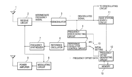
Fig. 2 is a block diagram showing a mobile
communication terminal according to a preferred embodiment
of the present invention;
Fig. 3 is a flowchart for explanation of the operation
of the mobile communication terminal according to the
present invention; and
Fig. 4 is an explanatory diagram showing an appearance
of the ad~ustment of a reference oscillator.
DETAILED DESCRIPTION OF THE PREFERRED EMBODIMENTS
Now, descriptions will be given in more details of a
preferred embodiment of the present invention with reference
to the accompanying drawings.
Fig. 2 is a block diagram showing a mobile
communication terminal according to a preferred embodiment
of the present invention. As is apparent from the
CA 02220817 1997-11-12
comparison of Fig. 1 with Fig. 2, this embodiment is
different from the prior art shown in Fig. 1 in that there
are provided a base station search circuit 11 and a
frequency offset generating circuit 12 that operates
according to its search result. Also, this embodiment is
different from the prior art in there is provided a switch
10 for swltching the operation of adjusting a reference
oscillator in an initial state at the time of turning on a
power supply to the frequency adjusting operation of the
conventional system using the frequency error detector,
after the base station is grasped, synchronization is
established, and spectrum de-spreading is enabled. Other
differences between the present invention and the prior art
except for the above differences become apparent as a
description goes ahead.
Fig. 3 is a flowchart for explanation of the operation
of the mobile communication terminal shown in Fig. 2.
Referring mainly to Figs. 1 and 3, a preferred embodiment of
the present invention will be described in more detail. It
should be noted that the detailed description of parts which
are not changed from those of the prior art in Fig. 1 will
be omitted here.
At an initial state where a power supply is turned on,
the switch 10 is connected to an initial setting side, that
is, an output of a frequency offset generating circuit 12
CA 02220817 1997-11-12
(Step S1 in Fig. 3), which is set to an initial setting
mode. A reference oscillator control circuit 5 is
initialized (Step S2 in Fig. 3), and in this state, the
output frequency of the reference oscillator is usually
greatly shifted from the frequency of a receive signal.
Fig. 4 shows its appearance. For example, the
frequency of a reference oscillator 6 is f1 with respect to
a target frequency fT. A range indicated by reference
symbol (1) in the figure is representative of a range in
which a base stration search is enabled when the frequency of
the reference oscillator is fl.
In this state, a base station search is first
conducted (Step S3 in the figure). As a result, if the base
station could not be grasped, an offset signal corresponding
to a frequency ~f is generated by a frequency offset
generating circuit 12, and the output frequency of the
reference oscillator 6 is shifted to f2 through the
reference oscillator control circuit 5 in Step S5.
With the above operation, the range in which the base
station search is enabled becomes a range (2). At this
stage, the base station search is again conducted. In Fig.
4, since no target frequency fT is contained in the range
(2), the base station search is again in failure. At the
next time, the frequency offset generating circuit 12 is
again allowed to generate an offset signal corresponding to
CA 02220817 1997-11-12
(frequency - 2 x ~f) in Step S5, and the output frequency of
the reference oscillator 6 is shifted to f3 through the
reference oscillator control circuit 5. As a result, the
range in which the base station search is enabled becomes a
range (3) of Fig. 4. In this situation, if the base station
search is further conducted, since the target frequency f~
is contained in the range (3) in Fig. 4, the base station
can be grasped. On the contrary, if the base station could
not be grasped even in the range (3), the offset signal
corresponding t~o 2 x ~f is now supplied in step S5.
If a grasp of the base station succeeds, the switch 10
is switched to an AFC side in step S6, the conventional
automatic frequency control as was described with reference
to Fig. 1 is started.
Also, a control signal which is obtained by frequency
adjustment which has been conducted during the previous
operation, that is, a control signal which is obtained when
the grasp of the base station succeeds is stored in a memory
13, so that it can be utilized as an initial value of a
succeeding initial frequency adjustment. According to this
mode, a period of time required for grasping the base
station immediately after the power supply is turned on can
be further reduced.
As was described above, according to the present
invention, the re~erence ~requency can be adjusted rapidly
CA 02220817 1997-11-12
and accurately even in a case where the conventional
reference frequency adjusting method is difficult to apply,
such as a initial state at the time of turning on the power
supply o~ the movable communication terminal using the CDMA
system. Hence, the present invention can provide a mobile
communication terminal which is capable of adjusting the
reference frequency rapidly and accurately without using the
TCXO which is expensive and high in accuracy.
Modifications of the invention herein disclosed will
occur to a p~erson skilled in the art and all such
modifications are deemed to be within the scope of the
invention as defined by the appended claims.