Note: Descriptions are shown in the official language in which they were submitted.
CA 02220883 1997-11-12
wo96138092 Pcr/Isg6/00593
MICROFABRICATED THERAPEUTIC ACTUATOR MECHANISMS
The United States Go~ Pnt has rights in this invention
pursuant to Contract No. W-7405-ENG 48 between the United States
D~,ent of Energy and the University of C~~liforni~ for the operation
of Lawrence Livermore ~:~h~ l Laboratory.
BACKGRMJND OF THE rNVENTION
The ~fesel-l invention relates to microstructures,
particlll~rly to electromech~nir~l micrcmerh~ni~m.~, and more
partic~ rly to microg.-~ers for use in catheter-based i.~lelv.o.~l;on~
thPr~pi~PS or remote micr~csemkly applir~tionc.
Micro~ctu~tors for remote and precise manipulation of
small objects is of great ~lller~sl in a wide variety of applir~tionc The
design and development effort of such microg-;~pel devices would be
useful in the art as such will apply to general microfabrication
terhniques and establish the infrastructure for microPnginPPring efforts
inrl~lin~ robotics, microterhnology, prevision PnginPPring~ defense,
energy, and biom~p~lir~l research, as well as use in me~lir~l applir~tion~,
such as for catheter-based int~ P~tion~l therapies and remote assembly
- or use of microm~rh~nir~l system.
When a portion of a blood vessel weakens, it bulges and
forms a ane~m, which is one of the main reasons for strokes as the
vessel finally collapses and opens. These aneuly~ms have tr~lition~lly
been treated by surge. ~, where the surgeol- will have to open up the area
of repair before aUe-,l~Lng to surgically repair the aneurysm by clipping
it. How~ver, many aneu~ - -s are at critical locations such as in the
brain and are either .lifficlllt and risky to operate on or it is simply
impossible. Por the last 20 years, pioneering doctors have used
illlelvPr~lior~l neuroradiology techniques to aid the treatment of brain
aneu.y~ Ls~ Long (1-2 meters) and narrow (i.e. 250,um to 500~m)
catheters are pushed through the arteries in the groin up to the brain to
reach the aneurysm. Existing catheter-based interventional instruments
CA 02220883 1997-11-12
W096~8092 P~~ f''~ 3
rely on simplistic and usually singular means of actuation. These
techniques, in~ ling balloon angioplasty, are well-established for large
vessel treatments such as in the heart. It is crucial that in order to extend
this medical practice into the sm~ r vessels such as those in the brain,
the catheter-based tools must be mini~tllri7ed. In the most recent
method, pl~timlm coils were selected to fill up the aneurysms due to its
ability to fill up irregular shapes and its resistance to electrolysis in the
vessels when it is charged. The coils are either pushed through the
cat~eter to the aneurysm by a guide wire or rele~e~ by the electrolytic
~iicsollltic~n of a solder joint between the guide wire of the catheter and
the therapeutic device, which for neurological treatments are
dyyro~ t~ly 25011m or less in diameter. Although the charging of the
coil causes elec~oll~rombosis around the coil, the time required to
release the coil is long (4 mins to 1 hr) and many coils are usually n~e~le-l
to fill tlp a regular size aneurysm. The extent to which the dissolved
m~pri~l affects the body is unknown and electrolysis sokl~ring requires
long terms of current in the brain and so~netimes is simply unreliable.
These ~iiffir~tlti~s ~resent potential life-threatening problems to the
patient for the sur~eol~ and ~ niri~n
Thus, there is a need for a micromerh~nicm which can fit
into a 25011m ~i~met~r area and which would enable the physician to
release and retrieve the coils or other therapy once it is r.ole~se-l at the
wrong time or location. The present invention satisfies this need by
providing a micrometh~nir~l release mechanism by which this
- procedure becomes a safer and more reliable alternative to surgery, and
which can fit into blood vessels of the brain, a 250~1m diameter area. The
electrome-h~ni~ ~l microstructures, including microgriyy~.s, can be
fabricated using known IC silicon-based techniques or precision
microm~hining, or a combin~tic-n of these techniques. While the
invention has application in various areas requiring a remotely actuated
microgripper, it has particular application in catheter-based
intervention~l therapies.
SUMMARY OF THE INVENTION
It is an object of the invention to provide an electro-
me- h~nir~l micro~,lipyel.
CA 02220883 1997-11-12
W096138092 P~-l/Lb~'~C~-~3
-3-
A further object of the invention is to provide a
micro~A~er with a large ~";pp;ng force, a relatively rigid structural
body, and flexibility in fl-nction design.
A f-urther object of the invention is to provide an
electromPrh~nir~l micromerh~nicm mounted at one end of a catheter
and which can be manipulated from the other end, thereby PY~en~ling
and illlyrovillg the applir~tic-n of catheter-based interventional
therapies.
Another object of the invention is to provide a
mi~ rogr;p~r capable of operating in an area as small as a 25011m
mpt~pr~ such as in the blood vessels of the brain.
Another object of the invention is to provide a
microgripper which can be used to integrate hP~tPrs and strain sensors
for remote active h~P~ting and feedback control.
Another object of the invention is to provide a
mi~:lo~ er which can be used as a biopsy tissue sampler, or for use as a
tip ~lpci~nerl for h~n~ilin~ micn~parls.
Another object of the ii~v~ntion is to provide a
mi~ogl;~per which has the ~olenlial to apply alten~aliv~ act~l~tion
mPrh~nicmc, either hydlaulic or simply thprm~l bimorphic.
Another object of the invention is to provide a
microgripper with a large gripping force (40mN), wherein actllati--n
thereof is generated by shape-memory alloy thin films and the stress
in~rerl can deflect each side of a mi~o~ er up to about 55~m for a
total ~,i;p~;ng motion of about 11011m.
Other objects and advantages of the present invention will
become a~aient from the following description and ~ccompanying
drawings. Basically, the invention involves an electromerh~nir~l
micr~ merh~nicm which can be l~tili7e~l in me-lirAl as well as non-
me~ic~l applications, and is particularly applicable for catheter-based
inl~ enlional therapies for the repair of aneuly~ll,s in the brain, or
other small blood vessels. The microgA~el of this invention has: 1) a
large ~A~ing force, 2) a relatively Agid structural body, 3) can be ~ltili7e-1
in a 250~Lm rli~meter area, 4) allows for flexibility in shaping the gA~ing
jaws, 5) can be used for biopsy sampling or for handling mi~oya. l~, 6)
has fast release and retrieve capabilities, 7) can be integrated with heaters
and strain sensor for remote active heating and feedback control, 8) may
CA 02220883 1997-11-12
W096t38092 PCT~B96/00593
be used with hydraulic or simple thPrmAl bimorphic actuation, and 9)
may be co~ cted using ~ ve,~lio~Al integrated circuit silicon-based
techniques or precision micromAt hin~, or both
BRIEF DES~ ON OF THE DRAW~GS
The ac~;v~ >al-r~lg drawings, which are in~;o~o~led into
and form a p_rt of the disclosure, illllctrAte e~ l~o~li...Pntc of the
invention and, together with the desc~;~Lon, serve to explain the
principles of the invention.
Figures lA and lB are cross-sertinnAl views of an
embo~lim~Pnt of the mi~;lv~ ~r using balloon activation, and shown in
the dosed and open pos;tionc~
Figure 2 is an exploded view of the Figures lA-lB
embo~1iment, with the b~llssm o~ le~1-
Figures 3A and 3B illustrate another embofliment of themicr~;l~r us~g a ~n f~ tweezer-iiKe a.Lvaion
Figures 4A and 4B are cross-sectiorl~l views which illustrate
another embo~limPnt of the micro~ el using a shape-memory alloy
(SMA) wire dicker.
Figure 5 is an exploded view of the Figures 4A~B
embo lim~Pnt with the SMA wire c~ tl~
Figure 6 is an emhoflimprlt of the invention using SMA
double coils.
Figure 7 is a ~reÇ~red embo liment of a silicon
microgripper made in accordance with the ~resent invention.
- Figure 8 is a cross~ertio~l view illustrating the ellt~ctic
bonding ~rocess.
Figures 9, 9A and 9B illustrate resistive heaters and
Plectrir~l feed~lrough for Figure 7 a micro~
Figures 10,10A and 10B illustrate an embo liment of the
heater of Figure 8A, with cross-sections as shown in Figure 10A and 10B
- greatly enlarged. -
Figures 11, 11A and 11B illustrate another emborlimpnt of
the heater of Figure 9, with the cross-sectionc of Figures 11A and 11B
greatly enlarged.
Figure 12 illusllales a force fee~lk~ control system for the
microgripper of Figure 7.
~,ll~ltU SHEET
CA 02220883 1997-11-12
W0 96/38092 PCT/II~g '~ ~ -~3
Figure 13 is a view of an SMA film activated microactuator
made in accordance with the invention for providing hydraulic
~res~ 2/fluid delivery from a microballoon.
DETAILED I~ESCRIPIION OF THE PREFERRED EMBODIMENTS
The invention is an elechronlerh~nical grip/release
microm~rh~nicm referred to thereinafter as a microgripper or
microrl~m~r. The micro~,ri~el has a large gli~ing force, a relatively
rigid shuchural body, and flexibility in flmcti~r ~l design such that it can
be used, for example, as a biopsy tissue s~mpler, a tip designed for
h~nrllin~ mi.~ s, or as a release/retrieval m~rh~ni~m for items such
as pl~ffnum coils or other materials in bulging portions of the blood
vessels, known as aneulysms. The micro~ er of this invention is
particularly useful to extend and improve the applir~tion of r~thPter-
based inle..~P.~ n~l therapies, and is capable of use in a 250~1m diameter
area, such as a small blood vessel of the brain. The micro~ ~r may be
consllucted with outer 5llrhre5 which can be used to integrate heaters or
strain s~co~ s for remote active heating and feedback control. One
embo-liment of the microgripper, for ~ lP, is of a silicon structure
and incc,l~orales shape-member alloy (SMA) thin films, and the stress
inrll~ l can deflect the sides thereof to enable a g~ ing motion of about
110~1m. The micro~;r;~L can be fabAcated by precision microm~rhining
or by terhniques lltili7e-1 in the fabri' ~tion of silicon-based integrated
.;ii~uils.
The ~lltimllm obje-;live of the grip/release merh~nicm or
microg~ er is to achieve the following: 1) the cross-section should fit
into a diameter as small as a 250~1m area (open and dosed); 2) the release
of materials into the blood vessels should be less than 10 seconds; 3) the
le.,.~ralure range should be between 0-C and 37~C; 4) current should be
less that 10 mA, for example, if electrical energy is used; 5)100%
reliability.
Using collve~l;or~l silicon bulk micromachining
terhni-lues a m~rh~nic~l damper or microgripper as illustrated in
Figures lA, lB, and 2 can be fabricated to include a cantilever structure
therein which, for example, is about 800~m in length and the total
height of the structure is 250,um. Then a silicon microballoon may be
tlttli7e-l to merh,~nic:3lly deflect the cantilever arms to clamp onto
foreign objects at the front end thereof, as seen in Figure lA and lB. The
~ =
CA 02220883 1997-11-12
.
W096/38092 P~ 5J,'00593
microballoons are well characterized and can withstand pressures of up
to 10 atm. Such microballoons have also been tested for use in human
blood vessels. As seen in Figures lA-lB and Figure 2, the balloon
activated microg~ ,el generally indicated at 10 comprises a pair of jaws,
grip arms, or gripping members 11 and 12, each having a plurality of
slotted cantilevers 13 and 14, a pusher pad 15 and 16, and ~ e ~ 17 and
18. For some app~ hon~ the pusher pads may be omitte~ The jaws or
g members 11 and 12 are bonded or oLllel -. ise secured together as
intli~ l at 19. An eYr~nti~hle device, such as a balloon 20, is positioned
between ~i~ing rrlemherc 11 and 12 and cor necte~l to a delivery tube or
cath~tor 21 which ~xt~rlds along the b~lloon path 22 (See Figure 2)
through which an activating fluid or gas is supplied to activate (expand)
the ball~ orl 20. Pusher pads 15 and 16 serve as balloon force points 23
(See Figure V~ and when fully expanded an end of the balloon may
exte~ l;~e~re~l~ the~sher pads 1~l6 as shown m Pigure lA.
With the balloon 20 in inactivated (unexpanded) position
as shown in Figure lA, the grippers 15 and 16. Upon activation
enlargement of the b~lloon 20, the outer ends of ~ yi~lg members 11
and 12 bend or flex outwardly at the location of slotted cantilevers 13 and
14 ~~A~-~in~ the ~;Li~l~l'~ 17 and 18 to separate, allowing the m~teri~l 24
retained therebetween to be removed therefrom, as shown in Figure lB.
The g~ members 11 and 12 may be constructed of
~ilicon~ Al~ .." nickel or other compatible metals, teflon or other
cc.~ le polymers, and cerarnics with a length of 0.8mm to 1.5mm,
and a width and combined height preferably not greater than about
25011m. The balloon 20 may be a silicone microballoon capable of
wilhs~ ing pressures of up to 10 atmospheres, supplied through the
tube 21, which may be constructed of teflon or other inert plastics having
a ~ meter of 80~1m to 400~1m The balloon 20 may be replaced with other
e~cp~n-l~hle devices. The bond 19 may be formed, for example, by
selective eutectic boncling The pusher pads 15 and 16 have, for example,
a thi~kn~s of 20~un to 4011rn, and E;r;~p~r~ 17 and 18 may have a
thit~kness of 9011m to 150~1m and length of 50~1m to 15011m. The slotted
cantilevers 13 and 14 may be composed of 3 to 10 slots having a width of
511m to lOOIlm and length of 50,um to 50011m. The slots of the
cantilevers may be straight or tapered along the length thereof. The
CA 02220883 1997-11-12
.
wo 96/38092 PcrlIs96loo593
m~t~?ri:ll that the gripper members 11 and 12 is constructed from must be
inert to the fluid or ch~mic~ involved.
The embodiment of Figures 3A and 3B utilizes a pair of
initial SMA thirr film hinges to open and close the grip arms or gripping
members acco~ding to the temperature the SMA thin film is exposed to.
The SMA thin films of Figures 3A and 3B can also be replaced by a heater
sandwiched by polyimide layer expands and ~lPfl~ctc the cantilever
clampers or g~ e~S.
As shown in Figures 3A and 3B, the microg~ er, generally
in~ tefl at 30 is composed of a pair of grip arms or ~ g members 31
and 32 forme~l~ for example, from silicon wafers, and each inrl~ l a
reduced thirkn~ss of cross-section area 33 and 34 and a pair of inwardly
directed spaced ~;~ D 35 and 36 only one gripper of each pair being
shown, which retain a mAteriAl or part 37, such as a stem of a platinum
cell (See Figure 3A). Thin films 38 and 39 are secured to gr;~;ng
me~e,;j 31 and 32 ~-ljacent the re~ e~l areas 33 and 34, with films 38
and 39 being cons~ cted of SMA or polyimide layers as described above.
The g~;y~ing members 31 and 32 are also provided with pusher pads 40
and 41. Upon heating of the thin films 38 and 39 by a heater, not shown,
the films ey~An~l I Allcin~ outward flexing or bending of the outer ends of
~l;yying members 31 and 32 at areas 33 and 34 causing the g~ el:~ 35
and 36 to s~arale (See Fig. 3B) whereby material 37 is removed
therefrom.
By way of ~y~mple, the grip arms or gripping members 31
and 32 may be constructed of silicon, or compatible metals, polymers, or
ceramics with an overall combined height and width thereof preferably
not to exceed 250~m, with the thickness of members 31 and 32 being 20
to 100~m, with re-i~lce~l areas 33 and 34 having a thickness of 5 to 15~1m,
and grippers 35 and 36 extending inwardly from members 31 and 32 a
t~nce of 20 to 50~m. The pusher pads 40 and 41 may for example,
having a thickness of 20 to 40~1m and depth (height) of 30 to 100~1m. The
thin films 38 and 39, if constructed of SMA, may be composed of Ni-Ti,
Ni-Ti~u, or other low temperature SMA, having a thickness of 2 to
511m, and if composed of polyimide, for example, having two layers of a
thickness of 3 to 1011m and length of 30011m to 50011m, which sandwich
therebetween a heater constructed of Ti-Au. Heating of the SMA films
38 and 39 is accornplished, for example, by integrating polysilicon heaters
CA 02220883 1997-11-12
wo 96/38092 Pcr/li~s~ c ~ - ~3
or direct resistive heaters of SMA, as described hereinafter with respect to
Figures 9 and 10, or by laser heating through optical fibers. Shape-
memory alloys are well known, as evidenced by U.S. Patent No. 5,061,914
issued October 29, 1991 to J. D. Busch et al.
The embodiment of Figures lA-lB and 3A-3B can also be
lltili7e~ to retrieve material or parts, such as platinum coils used to
repair aneurysms. These embodiment have advantages over prior
known mi-:rogri~ers that are Plectric~lly conductive (see C. J. Kim et al,
"Silicon-Processed Ov~rh~nging Microgripper", Journal of
MicroelectromerhAnicAi Systems, Vol. 1, No. 1, pp. 31-36, March 1992)
and can be used to manipulate biological cells or micro parts for
a~s-omhly.
The embodiment of Figures 4A-4B and Figure 5 is a
microgripper that is a normAlly open release mechanism (Figure 4B),
where an SMA wire is used as a latch to close the microgripper (Figure
4A), and when activated to click open the merh~ni~m. As shown, this
embo~limer t, generally in~licate~ at 50, comprises a pair of grip arms or
g.~ ng members 51 and 52, generally similar in construction to the
g m~mh.orS 11 and 12 of the Figures lA-lB embo~limf~nt, and are
provided with hook connectors 53 and 54, pusher pads 55 and 56, and
pairs of ~L;~pefs 57 and 58, only one each shown. A compressive thin
film 59 and 60 is secured in openings 61 and 62 of gripping members 51
and 52. Hook connectors 53 and 54 have opening 63 and 64 (see Figure 5)
through which an SMA wire 65 e~t~ncls (see Figure 4A) to "close" the
g members 51 and 52 and COlil~f~:SS the com~ressi~e thin films 59
and 60. Upon activation of the SMA wire 65, the wire is withdrawn
from openings 63 and 64 of hook connector s 53 and 54, as indicated by
the arrows 66 (see Figure 4B), whereupon the compressive thin fflms 59
and 60 expand causing the ends of gripping members 51 and 52 to flex or
bend outwardly. In the closed position (see Figure 4A) the pairs of
grippers 57 and 58 retain a material or part 67 therebetween, and upon
activation or rlirking open of the latch (hook connectors 53 and 54 and
SMA wire 65), the grippers 57 and 58 move outwardly allowing the
mAt~riAl or part 67 to be removed from therebetween. As in the
embo~iment of Figures lA-lB, the gripping members 51 and 52 are
bonded together as indicated at 68.
CA 02220883 1997-11-12
W096~8092 PCTA~5~ !0 - A3
By way of example, the gripping members 51 and 52, pusher
pads 55 and 56, and grippers 57 and 58 may be constructed and configured
as described above in the Figures lA-lB embo-liment The hook
cormPct~ 53 and-54 are composed of silicon, metals, polymers or ceramics
and secured, as by micromachining, and having a height of 80 to 200~1m,
width of 200 to 500~un and the openings 63 and 64 therein have a cross-
section of 80 to 380,um, width of 180 to 480~1m, and may be configured
other than square. The SMA wire 65 may be composed of Ni-Ti-Cu, Ni-
Ti, or Ni-Ti-Hf, having a cross-section and configuration which
COl. ~onds with the openings 63 and 64 of hook members 53 and 54.
The co~ ressive thin film 59 and 60 may be constructed of silicon
~lioxi~le, doped polysilicon, or polymers having a thickness of 3 to 811m,
and cross-section of 250 x 250 or 250 x 400~
Figure 6 illustrates a microgripper using two SMA micro-
coils, one to grip on to the stem of a plAtimlm coil, for example, and the
other one to push the pl~timlnl coil outwards to assure the release, the
micro-coils being se~:ured at one end to the tip of a guide wire, such as
used in ~ elel~-based inLe~ ;oI~1 therapies. As shown in Figure 6,
two SMA coils 70 and 71 are secured at one end to a guide wire 72. Coil
70, of substantially greater cross-section and of greater ~ m~ter than coil
71, extends (wraps around coil 71 and around an end of a stem 73 of a
platinum cell, for example, and retains or grips the stem 73. The coil 71
~ n~ between the tip 79 of guide wire 72 and end 75 of stem 73. Under
nc-rmAl con~litior~ the coil 70 retains the stem 73 from moving, and
upon activation the coil 71 expands pushing the stem 73 out of the coil
70.
By way of example, the larger coil 70 may be cons~-lcted of
SMA wire having a diameter of 50 to 7511m, a number of turns or wraps
ranging from 10 to 15, and constructed of Ni-Ti, Ni-Ti~u, or Ni-Ti-Hf.
The sm~ller coil 71 may be constructed of SMA wire composed of Ni-Ti,
Ni-Ti~u, and Ni-Ti-Hf, having a ~ met~r of 30 to 50,um, with the turns
or wraps ranging from 5 to 10. The micro-coils 70 and 71 may be secured
to guide wire 72 by b--n~ling, sol~l.oring, etc.
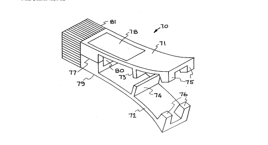
The ~rerei~ed embodiment of Figure 7 uses a combination
of silicon structure and SMA thin film, and is provided with a wiring
jacket for signal input. This embodiment provides a microgripper that
can be locally actuated at low temperatures (<100~C), with a large
CA 02220883 1997-11-12
W096/38092 PCTnB96/00593
- 10 -
ing force (10 to 40mN), a relatively rigid structural body, and
flexibility in functional design. Also, this microgripper has the capability
to lock the target gripping object. The actuation of the microgripper is
gPnPratP-l, for example, by NiTiCu shape-memory alloy thin films and
the stress in~ c~l can deflect each side of the microgripper up to 5511m
for a total g.i~ing motion of 110~1m. This opening motion co.les~onds
to a 20mN opening force on the tip of the gripper. In a~ition the
mi~o~ yel can work in a liquid environment. The opening jaws, the
pusher pads, and the hollow t~ nnPl are shaped by a combination of
precision sawing and bulk machinin~ of silicon. Two preprocessed
silicon wafers are prevision ~ nP-l and selectively bonded, using an Au-
Si el-tectic ~focess which involves ~ligning a mask on a wafer and
eva~oldling through the mask onto the gripper bonding portion, as
described in greater detail hereinafter with respect to Figure 8. The
mi~ er of Figure 7 is lmm x 20011m x 38011m in rlimpn~ic)n~ having
a pair of silicon cantilevers 12.511m thick, with 511m thick NiTiCu SMA
thin films deposite~l on the outer sides of the cantilevers or gripper arms
to provide ~ctll~tion of the microgripper. The SMA thin film can
generate act-~tinn stresses up to 500 MPa at transformation temperatures
between 30-C to 70-C, which is a lower temperature than all known
thermal bimorphic micro~,rippers. For experimPnt~l verific~tion~ the
micro~ er was ac~l~t~l by PYtprn~l hP~tin~ and a video tape was
~r~ared to ~iPmonctrate the opening and closing motions.
Referring now to a specific embo-limPnt as shown in Figure
7, the microgripper generally in~ ate~l at 70 in~ es a pair of silicon
cantilevers, gripper arms or gripping members 71 and 72, each member
71 and 72 having a 3011m wide pusher pad inrlil ~t~-l at 73 and 74,
respeclively, and a pair of 60 x 110 x 10011m3 gripping jaws or grippers 75
and 76. The ~,liy~ing members 71 and 72 are Au-Si eutectic bonded
together at an interface 77, and are each provided with an SMA thin film
78 and 79 on the outer surfaces or sides thereof. The cantilevers or
ping members 71 and 72 are constructed to define a 11011m wide
hollow channel 80 in the area of the bonded interface 77, which is in
commlmicati-~n with one end of a catheter, for example, on which the
micro~ er is mounted. The microgripper 70 is secured to a wiring
jacket, generally indicated at 81, for signal inputs.
CA 02220883 1997-11-12
W096/38092 PCT/lb~'~~-~3
The composition of the ~ ing members 71 and 72, the
SMA thin films 78 and 79, the eulectic bond 77, and the ~limen~ions of
the micro~ er 70 have been set forth above. By way of example, the
pusher pads 73 and 74 may have a thi~knP~ of 20 to 4011m and height of
80 to 100~m; with the gripper 75 and 76 having a height of 80 to 10011m,
and end cross-section of 70 x 150,um; and with the hollow channel 80
having a width of 100 to 25011m and height of 50 to 180~1m.
The fabrication of the micro~ per emborlimPntc of Figures
lA-lB, 3A-3B, 4A-4B, and 7, particularly Figure 7, allows the riPsignpr
some flexibility in shaping the gli~ g jaws as the targeting spel imPnc
dictate, and can either be used as a biopsy tissue sampler or a c~thPtPr tip
~1PC;~Pr1 for ~n~llin~ microparts. The outer surfaces of the
mi,.o~ er, particularly Figure 7, can be used to integrate hP~tPrs or
strain s~l~col;, for remote active hP~ting and possible feedback control as
riPCI rihe~l hereinafter with respect to Figures 9-12. The hollow channel of
the Figure 7 embo~limPrlt has the potential for either wire connection or
njection of liquids and therapeutic me~ e. Another important
advantage is the poscihility to apply alternative actuation merh~nicm~
on the mk.o~ er structure, either hydraulic or simply thPrm~l
bimorphic. Many creative ~Psignc of practical microgrippers for various
applic~ti~ can be conceived using this basic approach. Fabril ~tion
process steps can be highly automated and batch fabrication of the
microgl;~ers will reduce the m~nl1f~cturing cost.
App!ic~ti- rl~ of the Figure 7 microgripper indude
- assembling small parts for m~nllf~cturing~ minimally-invasive in vivo
biopsy tissue s~mpling~ catheter-based endovascular therapeutic
~rocedures, and remote h~n-llin~ of small particles in extreme
ellvir~,l....ent~ (high/low pressures, hazardous fluids, etc.).
The microfabric~tion process for the Figure 7 embodiment
can be categorized into bulk micromachining, fine alignment, etching,
and Ni-Ti-Cu SMA thin film deposition. As set forth above, a specific
embo~imPnt of the Figure 7 type microgripper is 1000 x 200 x 380~Lm3 in
dimension. Each silicon cantilever (72 and 73) is 125~1m thick and 5~1m
Ni-Ti-Cu SMA thin films (78 and 79) are deposited on the outer surfaces
of the cantilevers for actuation thereof. The pusher pads (73-74) are
30~1m wide while the ~ illg jaws (75-76) are 60 x 110 x 100~1m3. The
hollow ~ h~nnPl 80 is 110,um wide and 175~m in height. The gripping
CA 02220883 1997-11-12
WO 96138092 P~ b5~'1;1;~553
~ 12-
jaws, pusher pads, and hollow channel are shaped by a combination of
precision sawing and bulk machining of silicon, and thus can be batch
fabri<~te~l The connection of the microgripper to external leads and
milli-end effectors (as exemplified in Figure 9) requires assembly and
therefore does not allow for batch fabrication. However, there is an
ongoing effort to develop assembly techniques for packaging.
The cantilevers or gripper arms (71-72) of the microgripper
are fabricated on two silicon wafers. This ~rocess starts with two 10011m
thick (110) p-type silicon wafers, which are ground and polished from a
width of 200,um to an overall width of 38011m. The cQmmon masking
film for p~t~ g and etch silicon was lo00A of silicon nitri~o
A test ~all~ ll is essenti~l to identify the exact (111) plane as
opposed to the wafer flat, which is typically offset 2~-3~. ~lignm~ont
targets are imprintefl on each of the silicon wafers using this crystal
plane identifying pattern to ensure the subsequent ~ligning to the exact
crystal planes. Two types of ~li~m~nt targets must be ~l~finell, one to
carry out front-to-back ~lignment and another etched through the wafers
to provide holes for precise pin mPrh~nic~ lignment~ for eutectic
bon~ling Dicing line (211m deep) are then p~tt~rn~rl on the backside of
each wafer. On the front side of each wafer, saw cut t h~nn~l guide lines
are p~ rn~rl for the precision saw to form the silicon cantilevers (71-72)
and the pusher pads (73-74). These patterns are imprinted by etching the
silicon down lllm. After reapplying the masking silicon nitride,
lathography is carried out for the ~,ip~ing jaws (75-76) and the hollow
l h~nnel (80). The silicon wafers are then etched in 44% KOH, creating
vertical walls 85~1m deep. The silicon nitride mask is then stripped and
ready for the precision saw, such as a model 780 by Kulicke & Soffa, with
positionin~ accuracies as high as 2.511m. Precision sawing was chosen to
avoid the anisotropic etching limitations of silicon that does not allow
vertical wall etch channels 90~ apart without careful corner
compPn~tic-n and s~rrifice of fini~he-i sllrf~ces Since the width of the
two cut channels are 20011m and 40011m, respectively, the blade selected
was 20011m thick. The wider cut ~ h~nn~l (400~1m) was formed by making
two adjacent saw cuts. The saw was indexed to leave a pusher pad (73-74)
width of 3011m. For careful control of the cut depths, it is I-ecess~ry to
index the depth from the bottom of the wafer. Furthermore, it is ideal to
dress the blades on rougher surfaces to achieve the vertical edges. The
CA 02220883 l997-ll-l2
W096138092 PCT~95i'~~593
-13-
pair of silicon cantilevers or gripper arms (71-72) formed from the silicon
wafers are now reading for bonding.
Bonrlin~ of the cantilever or gripper arms of Figure 7, for
example, is carried out using Au-Si eutectic bon~ling~ whereby selective
areas of bonding at a low temperature (<400~C) is achieved. The silicon
microstructures, such as the gripper arms of Figure 7 can be bulk
micromachined on two silicon wafers, as described above, and then
ellt~chr bonded, which enables (1Psigner to ~l~signer minimal gap
microstructures that can also be applied as c~r~t~it~nre sensors/~c~ tc-rs
and microfl~ lirc systems with tight seals.
Using Au-Si eutectic bonding a microstructure, composed
of the two silicon m~chin~-l wafers, such as illustrated in Figure 7 may be
f:~hrit :~te~1 as illustrated in Figure 8. On each cantilever 82 framed from a
silicon wafer, Ti/Au pads, generally in~ic~te~l at 83, 500 x 500~1m in area
for example, are deposited by electron beam (E-Beam) evaporation
in~ te-l at 84, by arrows and patterne~ through shadow masks 85 and
86, such as illustrated in Figure 8. The Ti layer 87 is an adhesive layer
and also serves as a diffusion barrier for Au layer 88. The thirkn~ss of
the pads 83 are, for ~Y~mple, 500A for Ti (layer 87) and 1,um for Au (layer
88). The Annea1ing temperature is 370~C to 390~C which is above the
363~C eutectic point to assure the interface to liquidify. Soaking at this
temperahlre for 5 miml~s is necessaL~. The shadow masks 85-86 are
e~ elllly fabricated by etching windows out of (100) silicon wafers. By
~ligning the shadow masks to the wafer only areas coated with Ti/Au
- will be bonded together. The m~ting silicon wafers should have a fully
ne~l silicon surface where the bonding is to occur. The wafers are
then ~ressul,zed together and held in low vacuum (nomin~lly 10-4
Torr) and so~ke-l, for example, at 380~C for three (3) minutes. An
acoustic image of an array of Ti/Au eutectic bonding pads 83 seen
through a pair of 2 inch silicon wafers showed that a highly uniform and
solid bond has been formed. The Au-Si bond strength was measured in
an instron pull test, where 9 eutectic bond pads were pulled and failed at
pull stress of 5.5 GPa. The eutectic bond areas were intact, as fracturing of
the silicon surrol-n~ling the bond areas occurred in the process.
During the bonding process, rnech~nical alignrnent using
precise diameter pins were applied to ensure controlled processing and
~,~vent shattering of the fragile thin cantilevers. The bonded pair of
CA 02220883 1997-11-12
wo 96/38092 Pcr/~ - c ~~93
- 14-
cantilevers (71-72) are now ready for deposition of the SMA thin films
(78-79).
The SMA thin films are composed of Ni-Ti-Cu deposited
using a mixed dc magnetron sputtered deposition, the details of the
mixed splltt~rinE process are set forth in copending application Serial
No. 08/(IL-9463), filed May 1995, entitled, "Multiple Source Deposition Of
Shape-M~mc)ry Alloy Thin Films" and ~Csignerl to the ~signPe of this
appli- Atis~n In that sputtering process, three (3) separate targets are used
to s~,tlel the alloy such that the power can be individually controlled to
actively determin~ the alloy composition- The thin film was deposited
at 505~C, for ~Y~mple, so that it is in sihl aI ne~le~l to relieve the residual
stress. The SMA fflm was initially deposited seqll~nti~lly on the outer
sides or surface of the cantilever arms (71-72) of Figure 7, for example, so
that one side is ~nne~le~l twice at 505~C, but preferably deposition of the
SMA film prior to bonding of the cantilever arms would reduce th~rm~l
stress in the film. The following sets forth a concise process sequence for
fAhri- ,~hng a micro-actuator, such as illustrated in Figure 7, the sequence
includes:
a) pattern crystal plane test marks, align targets and
nm~nt holes.
b) pattern saw cut ~h~nnel guide lines.
c) p~ttern silicon etch channels following the (111) plane
direction.
d) anisotropic etching of the silicon etch channels by KOH.
e) shadow mask ~lignment to wafer, and deposition of
Ti/Au film.
f) merh~nirAl pin alignmerlt and eutectic bonding at 380~C
(3 min.) and 10-4 Torr.
g) m~gn~tron sputter deposition of Ni-Ti-Cu films on both
sides with in situ ~nne~ling at 505~C.
h) dice up individual microgrippers.
The microgripper of Figure 7, is actuated using the dc
magnetron s~Llered nickel-titanium-copper-shape memory fil~n.
Shape memory acttl~tion is based on a crystalline phase transform~tion
in which the low temperature phase (martensite) is easily and reversibly
~leform~ble via twins, while the high temperature phase (austenite) has
one rigid configuration. The Ni42TisoCug alloy transforms just above
CA 02220883 1997-11-12
wo96/38092 PcrlIsg6/oosg3
body temperature (37~C), making it useful for implantable medical
devices, and has a narrower hysteresis than binary nickel-titanium
which increases ~ffiri~ncy and improves response time. Purthermore,
the ~ liti~n of copper makes the trar ~form~tic)n temperature less
sensitive to film composition.
In the microgripper application, actuation occurs by the
recovery of tensile residual stress in the memory film, the data thereof
being obtained by measuring substance curvature as a function of
temperature. The film, which is deposited at 500~C, develops a tensile
thermal stress as it is cooled after deposition. When cooled below the
temperature at which the martensitic l-dnsro~ ation starts, the th~rm~l
stress in the film can relax by twin-related deformation. This tensile
therm~l stress can be recovered by heating the film. Thus, the silicon
og~ r cantilevers act as bias springs which are opened by the
contracting shape-memory film (78-79) when heated, then ~l~flect~l back
to a reutr~l position and stretch the shape-memory film when cooled.
Films with up to 500 MPa recoverable stress have been deposited, but the
film on the cantilevers of Figure 7, for example, have a recoverable stress
of 375 MPa. Testing of the stress in~ cerl by the Ni-Ti-Cu film was
measured by a Tencor FLX-2320 laser system, which measures the
curvature in-lllce~l by the film on an Si sul~slldle, which is translated into
stress.
In order to evaluate the gripping force induced by the Ni-Ti-
Cu SMA filrn, an equivalent model with an opening force at the tip was
- assumed. By applying bimetallic stress equations, the relation between
the Ni-Ti~u film stress and the ~lpflection of the gr;~per tip was
~'~l~ll?,te.l Por a film thi~kness of 5~m, the ~ieflechorl is calclll~te~l to be53~n. Experiment~l results showed the gl;pper opening to 55,um when
fully actll~terl Using the equivalent model, it was found that it requires
20mN to deflect the microgripper to 5511m. Therefore, a gripping force of
40mN (20mN on each cantilever) is applied for a fully open
microgripper.
The heating of the microgripper of Figure 7 was applied by
an integrated circuit (IC) fabricated thin film resistor heater pad, as
~l~s~ribe-1 in greater detail with respe* to Figures 10 and 11. The heater
pad is placed on the microgripper cantilevers and current is applied, the
heat is transferred from the heater to the Si gripper cantilevers for phase
CA 02220883 l997-ll-l2
W096/38092 PCTA~~.'C-~.3
-16-
transform~tion in the Ni-Ti-Cu film to take place. Thus, remote active
h~ting of the SMA film can be accomplished.
Also, the microgripper of E~igure 7 is being integrated with
strain sensor for feedback control as described hereinafter with respect to
Figure 12.
Figures 9, 9A and 9B illustrate packaging of the
microgripper of Figure 7 on a c~th~t~r. Components similar to those of
Figure 7 are given corresponding reference numerals. The microgripper
70 is ~lectric~lly connected to a wiring jacket 81' via a SMA film resistive
heater, generally indicated at 90 on cantilever 71 and having contract
pads 91 and 92, which are connecte~l via leads 93 and 94 to contact pads 95
and 96 on cor~ rhve films 97 and 98 such as copper, bonded to a
polymide member 99, of an electrirAl feedthrough ribbon generally
in~ terl at 100. As in~ic~te-l by leads 93' and 94', an i~l~ntir~l resistive
heater and ~lectric<ql connection arrangement is provided between
cantilever 72 of microgripper 70 and the cor~ lctive film on polymide
member 99' of wiring jacket 81. The polymide members 99 and 99' and
~csori~t~-l copper films are connected to insulated feedthrough wires
101/102 and 101'/102' of ribbon 100, and are located within a cat~et.or
tube 103 (see Figure 9A). The polymide members 99 and 99~
protruding end sections 104 and 104' which, as indicated by the arrows
105, extend into the hollow channel 80 of microgripper 70. The wiring
jacket 81' is secured to microgripper 70 by a heat shrink tube 106 (see
Figure 9B).
The resistive heaters 90~ of Figure 9 located on cantilevers
71 and 72 of the microgripper 70 may be of the type illustrated in Flgures
10, 10A and 10B or of the type illustrated in Figures 11, 11A and 11B, each
having piezoresistive feedback capabilities.
In the Figure 10 embo~liment, the resistive heater 90
inrlll~e~ contact pads 91 and 92, as in Figure 9, with resistive wires 107
being in electrical contact with pad 91 and resistive wires 108 being in
contact with pad 92. Figure 10A is a greatly enlarged section of Figure 10
and composed of a silicon beam (cantilever 71), SMA resistive wires 107,
108, 107, of resistive heater 90, between which are layers 109 and 110 of an
oxide, on top of which are layers 111 and 112 of polysilicon (poly-Si), and
on top of which are sections of the SMA thin film 78, covered by an
CA 02220883 l997-ll-l2
W096~8092 PCT/L~ g3
-17-
oxide or protective layer 113. Figure 10B is an enlarged cross-sectional
side view of the Figure 10 embodiment.
The resistive heater 90 of Pigures 11, 11A and 11B is
generally similar-to the Figure 10 embo~linl.ont, and similar reference
numbers will be lltili7e~l In Figure 11, the resistive heater 90 includes
contact pads 91 and 92, with resistive wires 107 conn~cte~ to pad 91 and
resistive wires 108 connected to pad 92, as in the Figure 10 embolliment
Figure 11A is a greatly enlarged view of a section of Pigure 11 and
composed of a silicon beam (cantilever) 71, an oxide layer 114, a pair of
polycilit~or e (poly-Si) layers 115 and 116 on which is deposited oxide
(I.TO) layers 117 and 118, the SMA thin film 78 and an oxide or
~rolective layer 113. Figure 11B is an enlarged cross-sectional side view
of the Figure 11 embo~ Pnt-
Figure 12 5rhpm~tir~lly illustrates a force fee~ih~c k control ofthe micro~ ~r 70 of the Figure 7 embodiment, and similar
components are given cor~ onding reference numerals. A s~n~in~
film 120 is deposited on a cantilever 71 and is connected via a strain-to-
stress cor.v_.;iion, indicated at 121, as discussed above, to a specified force
in~lir~t~r 122, the output of which is directed through signal processor
(amplifier) 123 to an ~rtl~atic-n film (SMA film 78). While not shown,
the lower cantilever 72 is provided with a similar arrangement.
The Figure 7 embo~im~nt can be modified to provide a
hydraulic pressure/fluid delivery system, as illustrated in Figure 13.
Here, cantilevers 125 and 126 of a microactuator 70' are provided with
- SMA thin films 127 and 128, respectively, with cantilevers 125 and 126
being ronn~rte~l by a section 129 having an opening, not shown, therein.
A microballoon 130 is position intermediate one end 131 and 132 of
cantilevers 125 and 126, while the other end 133 and 134 thereof is
provided with grippers or jaws 135 and 136. Upon actuation, ends
131/132 of the cantilever move inwardly, as indicated by the arrows,
while the ends 133 and 134 move outwardly, as indicated by the arrows,
whereby fluid within the microballoon 130 is forced therefrom as
n~ terl by the arrows 137, thereby delivering the fluid 137 to a point of
use.
It has thus been shown that the present invention provides
an electromechanical micromechanism (either IC silicon-based or
precision micromechanical) which will, for example, extend and
CA 02220883 l997-ll-l2
W096/38092 PCT~B96'~'g3
-18-
improve the application of catheter-based interv.ontit-n~l therapies for
the repair of arterio-aneurysms in the brain or other interventional
clinical therapies. The microgripper of this invention, in addition to
rr~e~lir~l applir~tic~nç, has non-medical uses, such as micro assembling
and for remote and precise manipulation of small objects, and has the
capability to operate in small areas having 250,um diameters, such as
small blood vessels.
While particular embo~iim~ntç~ m~teri~lç, parameters, etc.,
having been set forth to exemplify the invention, such are not int~n~
to be limi*ng Modifications and changes may become apparent to those
skilled in the art, and it is intended that the invention be limited only by
the scope of the appended claims.