Language selection

Search

Patent 2220966 Summary

Third-party information liability

Some of the information on this Web page has been provided by external sources. The Government of Canada is not responsible for the accuracy, reliability or currency of the information supplied by external sources. Users wishing to rely upon this information should consult directly with the source of the information. Content provided by external sources is not subject to official languages, privacy and accessibility requirements.

Claims and Abstract availability

Any discrepancies in the text and image of the Claims and Abstract are due to differing posting times. Text of the Claims and Abstract are posted:

  • At the time the application is open to public inspection;
  • At the time of issue of the patent (grant).
(12) Patent Application: (11) CA 2220966
(54) English Title: MULTIPLEXER, PROTECTION SWITCH UNIT, TELECOMMUNICATIONS NETWORK AND A MULTIPLEXING RELATED METHOD
(54) French Title: MULTIPLEXEUR, UNITE DE COMMUTATION DE SECOURS, RESEAU DE TELECOMMUNICATIONS ET PROCEDE DE MULTIPLEXAGE
Status: Dead
Bibliographic Data
(51) International Patent Classification (IPC):
  • H04J 3/02 (2006.01)
  • H03K 17/62 (2006.01)
  • H04J 3/04 (2006.01)
  • H04J 3/10 (2006.01)
  • H04J 3/14 (2006.01)
(72) Inventors :
  • BLADH, MATS (Sweden)
(73) Owners :
  • TELEFONAKTIEBOLAGET LM ERICSSON (Not Available)
(71) Applicants :
  • TELEFONAKTIEBOLAGET LM ERICSSON (Sweden)
(74) Agent: MARKS & CLERK
(74) Associate agent:
(45) Issued:
(86) PCT Filing Date: 1996-05-22
(87) Open to Public Inspection: 1996-12-05
Availability of licence: N/A
(25) Language of filing: English

Patent Cooperation Treaty (PCT): Yes
(86) PCT Filing Number: PCT/SE1996/000658
(87) International Publication Number: WO1996/038939
(85) National Entry: 1997-11-13

(30) Application Priority Data:
Application No. Country/Territory Date
9502011-1 Sweden 1995-06-01

Abstracts

English Abstract


There is provided a multiplexer which in a multiplexing process selects an
output signal from a plurality of input signals, a protection switch unit
which includes one such demultiplexer and a telecommunications network which
includes one such protection switch unit, the multiplexer has an output (OUT+,
OUT-) and at least two inputs (IN1+, IN1-, IN2+, IN2-) where two input signals
corresponding to the inputs are received. A first connection point (IN1+,
IN2+) in each input is connected to a first transmission line (TLINE_1) via a
respective first controllable signal forwarding device (Q1, Q2). An externally
controllable switch means (S2, S1) is also connected to each output for
forwarding a signal or at least a part thereof delivered to said input to a
first transmission line (TLINE_1). The first transmission line (TLINE_1) is
connected to a first connection point (OUT+) in the output, where a signal of
good quality is obtained.


French Abstract

L'invention concerne primo un multiplexeur qui sert, au cours d'un processus de multiplexage, à sélectionner un signal de sortie parmi plusieurs signaux d'entrée, secundo une unité de commutation de secours qui comporte ledit démultiplexeur et tertio un réseau de télécommunications comportant ladite unité de commutation de secours, ledit multiplexeur ayant une sortie (OUT+, OUT-) et au moins deux entrées (IN+, IN-, IN2+, IN2-) qui reçoivent chacun un signal d'entrée respectif. Un premier point de connexion (IN1+, IN2+) au niveau de chaque entrée est relié à une première ligne de transmissions (TLINE_1) par l'intermédiaire d'un premier dispositif manoeuvrable d'acheminement des signaux (Q1, Q2). Un organe de commutation à commande externe (S2, S1) est également relié à chaque sortie pour l'acheminement d'un signal ou au moins d'une partie de signal reçu au niveau de ladite entrée vers une première ligne de transmission (TLINE_1). Cette première ligne de transmission (TLINE_1) est reliée à un premier point de connexion (OUT+) de la sortie, où l'on obtient un signal de bonne qualité.

Claims

Note: Claims are shown in the official language in which they were submitted.


12


CLAIMS
1. In multiplexing processes, a method of selecting an output from a plurality of input
signals, wherein at least two input signals are received on inputs (IN1+, IN1-, IN2+,
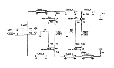
IN2-) corresponding to said signals, characterized by conducting selectively one of
the input signals or at least a first part of one of said signals from a first connection
point (IN1+) in one of the inputs to a first transmission line (TLINE_1) via a first
controllable signal forwarding device (Q2; D2), wherewith said input signal or said first
part of said input signal is obtained from said first transmission line as an output signal
or a first part of an output signal of good signal quality.

2. A method according to Claim 1, characterized in that the input signals each
includes a first and a second part and the output signal also includes a first and a
second part, wherein the second part of said input signal is conducted, at the same
time as the corresponding first part, from a second connection point (IN1-) in said one
input to a second transmission line (TLINE_2) via a second controllable signal
forwarding device (Q3; D4); and in that the second part of the output signal is obtained
from said second transmission line.

3. A method according to any one of the preceding Claims, characterized by
controlling the signal forwarding devices (Q2, Q3, Q1, Q4; D2, D4, D1, D3) connected
to the inputs (IN1+, IN1-, IN2+, IN2-) to forward the input signals from the inputs to said
transmission lines (TLINE_1 and TLINE_2) by an externally controlled switch (S2, S1)
corresponding to each input.

4. A method according to any one of the preceding Claims, characterized by
amplifying the output signal obtained from said transmission lines (TLINE_1 and
TLINE 2).

5. A multiplexer having at least two inputs (IN1+, IN1-, IN2+, IN2-) and an output
(OUT1+, OUT1-), wherein a first connection point (IN1+, IN2+) in each input is


13


connected to a common line (TLINE_1) via a respective first controllable signal
forwarding device (Q2, Q1; D2, D1), wherein there is connected to each input an
externally controlled switch (S2, S1) which functions to control said first signal
forwarding device to forward a signal or a first part of a signal delivered to said input to
said common line, characterized in that the common line (TLINE_1) is a first
transmission line which is also connected to a first connection point (OUT+) in the output.

6. A multiplexer according to Claim 5, characterized in that a second connectionpoint (IN1-, IN2-) in each input is connected to a second transmission line (TLINE_2)
via a respective second controllable signal forwarding device (Q3, Q4; D4, D3),
wherein said second transmission line is connected to a second connection point
(OUT-) in the output, and wherein said switch (S2, S1) also controls said second signal
forwarding device.

7. A multiplexer according to Claim 5 or Claim 6, characterized in that each of said
transmission lines (TLINE_1, TLINE_2,) is a microstrip mounted in the multiplexer
circuit board.

8. A multiplexer according to any one of Claims 5-7, characterized in that each of the
transmission lines (TLINE_1, TLINE_2,) is a parallel plane conductor mounted in the
multiplexer circuit board.

9. A multiplexer according to any one of Claims 5-8, characterized by an amplifier
(D_AMP) connected between one end of the transmission lines (TLINE_1, TLINE_2)
and the output (OUT+, OUT-) for amplifying the signals obtained from said
transmission lines.

10. A multiplexer according to anyone of Claims 5-9, characterized in that the signal
forwarding devices (Q1, Q2, Q3, Q4) are transistors, wherein the emitter is connected
to the connection points (IN2+, IN1+, IN1-, IN2-) in corresponding inputs via a resistor

14

(R1, R2, R4, R3), the collector is connected to the transmission lines (TLINE_1,TLINE_2), and the base is earthed with respect to the signal delivered to the
connection point in a corresponding input.

11. A multiplexer according to any one of Claims 5-9, characterized in that the signal
forwarding devices (D1, D2, D3, D4) are
diodes.

12. A multiplexer according to any one of Claims 5-11, characterized in that thetransmission lines (TLINE_1, TLINE_2) are terminated with a respective resistor (R12,
R44, R7, R45).

13. A protection switch unit (4) including a multiplexer, which has at least two inputs
(IN1+, IN1-, IN2+, IN2-) and an output (OUT+, OUT-), wherein a first connection point
(IN1+, IN2+) in each multiplexer input is connected to a common line (TLINE_1) via a
respective first controllable signal forwarding device (Q2, Q1; D2, D1), wherein also
connected to each input is an externally controllable switch means (S2, S1) which
functions to control said first signal forwarding device to forward to the common line a
signal or at least a part thereof applied to the input, characterized in that the common
line (TLINE_1) is a first transmission line which is also connected to a first connection
point (OUT+) in the multiplexer output.

14. A unit (4) according to Claim 13, characterized in that a second connection point
(IN1-, IN2-) in each multiplexer input is connected to a second transmission line
(TLINE_2) via a respective second controllable signal forwarding device (Q3, Q4; D4,
D3), wherein second transmission lines are connected to a second connection point
(OUT-) in the multiplexer output, and wherein said switch means (S2, S1) also function
to control said second signal forwarding devices.


15. A unit (4) according to any one of Claim 13 or Claim 14 characterized by an
amplifier (D_AMP) connected between one end of the transmission lines (TLINE_1
TLINE_2) and the multiplexer output (OUT+,OUT-) for amplifying signals obtained from
said transmission lines.

16. A unit (4) according to any one of Claims 13 - 15 characterized in that the signal
forwarding devices (Q1, Q2, Q3, Q4) at each multiplexer input are transistors wherein
the emitter is connected to the connection point (IN2+, IN1+, IN1-, IN2-) in respective
inputs via a respective resistor (R1, R2, R4, R3), wherein the collector is connected to
the transmission line (TLINE_1 TLINE_2), and wherein the base is earthed with
respect to the signal delivered to the connection point in a corresponding input.

17. A unit (4) according to any one of Claims 13 - 15 characterized in that the
multiplexer signal forwarding devices (D1, D2, D3, D4) are diodes.

18. A unit (4) according to any one of Claims 13 - 17 characterized in that the
multiplexer transmission lines (TLINE_1, TLINE_2.) are mounted on a multiplexer
circuit board and terminated with a respective resistor (R12, R44, R7, R45).

19. A telecommunications network that includes two or more lines connected to anexchange (1) via a respective terminal access unit (3), wherein each line is also
connected to a protection switch unit (4) which, in turn, is connected to the exchange
via a reserve terminal access unit (5), wherein the protection switch unit includes a
multiplexer that has an input (IN1+, IN1-, IN2+, IN2-) for each line and an output
(OUT+, OUT-) wherein a first connection point (IN1+, IN2+) in each multiplexer input is
connected to a common line (TLINE_1) via a respective controllable signal forwarding
device (Q2, Q1; D2, D1), wherein each input is also connected to an externally
controlled switch means (S2, S1) for controlling said first signal forwarding device to
forward to the common line a signal or at least a part of said signal delivered to said


16
input, characterized in that the common line (TLINE_1) is a first transmission line
which is also connected to a first connection point (OUT+) in the multiplexer output.

20. A telecommunications network according to Claim 19, characterized in that a
second connection point (IN1-, IN2-) in each input of the multiplexer included in the
protection switch unit (4) is connected to a second transmission line (TLINE_2) via a
respective second controllable signal forwarding device (Q3, Q4; D4, D3), wherein said
second transmission line is connected to a second connection point (OUT-) in themultiplexer output, and wherein said switch (S2, S1) also controls said second signal
forwarding device.

21. A telecommunications network according to any one of Claims 19 or 20,
characterized by an amplifier (D_AMP) connected between one end of the
transmission lines (TLINE_1, TLINE_2) and the multiplexer output (OUT+, OUT-) for
amplifying signals obtained from said transmission lines.

22. In a multiplexing process, a method of selecting an output from a plurality of input
signals, wherein at least two input signals are received on inputs corresponding to said
signals, wherein one of the input signals or at least a first part of one of said signals is
conducting selectively from a first connection point in one of the inputs to a first
transmission line via a first controllable signal forwarding device, wherewith said input
signal or said first part of said input signal is obtained from said first transmission line
as an output signal or a part of an output signal of good signal quality.

23. A multiplexer having at least two inputs and one output, wherein a first connection
point in each output is connected to a common line via a respective first controllable
signal forwarding device, wherein there is connected to each input an externallycontrolled switch which functions to control said first signal forwarding device to
forward to said common line a signal or a first part of a signal delivered said to input,

17

and wherein the common line is a first transmission line which is also connected to a
first connection point in the output.

24. A protection switch unit including:
a multiplexer which has at least two inputs and one output,
wherein a first connection point in each multiplexer input is connected to a common
line via a respective first controllable signal forwarding device,
wherein also connected to each input is an externally controllable switch means which
functions to control said first signal forwarding device to forward to the common line a
signal or at least a part of a signal delivered to the input, and
wherein the common line is a first transmission line which is also connected to a first
connection point in the multiplexer output.

25. A telecommunications network that includes:
two or more lines connected to an exchange via a respective terminal access unit,
wherein each line is also connected to a protection switch unit which, in turn, is
connected to the exchange via a reserve terminal access unit,
wherein the protection switch unit includes a multiplexer that has an input for each line
and an output,
wherein a first connection point in each multiplexer input is connected to a common
line via a respective controllable signal forwarding device,
wherein each input is also connected to an externally controlled switch means for
controlling said first signal forwarding device to forward to the common line a signal or
at least a part of a signal delivered to said input, and
wherein the common line is a first transmission line which is also connected to a first
connection point in the multiplexer output.

Description

Note: Descriptions are shown in the official language in which they were submitted.


CA 02220966 1997-11-13
WO 96/38939 PCT~SE96/00658


MULTIPLEXER, PROTECTION SWITCH UNIT, TELECOMMUNICATIONS
NETWORK AND A MULTIPLEXING REL~TED METHOD

FIELD OF INVENTION
.
The present invention relates to a multiplexer, a protection switch unit which includes
one such multiplexer, a telecommunications network which includes one such protec-
tion switch unit, and a multiplexing related method. More specifically, the invention
relates to the aforesaid devices and method in respect of single or differential0 multiplexing signals and preferably of the CMI type, at transmission speeds above
about 100 MbiVs and preferably in the range of about 140-155 Mb/s.

DESCRIPTION OF THE BACKGROUND ART

In telecommunications networks, a plurality of signal lines are often connected to an
exchange through the medium of a respective terminal access unit. These terminalaccess units are relatively expensive and complicated units and can sometimes break
down. For this reason, the network includes at least one protection switch unit which is
connected bet~veen the signal lines and a reserve terminal access unit connected to
20 the exchange. The unit includes a multiplexer or selector whose inputs are connected
to the signal lines and whose output is connected to the reserve terminal access unit.
When a regular terminal access unit cannot be used for some reason or another, the
multiplexor in the protection switch unit is controlled to forward to the reserve access
unit the signal corresponding to the normal terminal access unit.
2'j
Good signal quality and controlled amplification is needed when selecting or multiple-
xing signals having transmission speeds in the region of about 140-155 Mb/s. In this
regard, the pulse shape of the output signal is often required to be the same as the
pulse form of the input signal and the level of the output signal required to be the same
3 cl as it would have been if the signal had not passed through the multiplexer.

CA 02220966 1997-11-13
WO 96138939 I~ CQ


Problems with mismatching between components and conductors can easily occur in
such multiplexers at such high transmission speeds, therewith greatly impairing signal
quality.


A number of standard circuits exist for multiplexing signals having bit rates of up to
about 30 Mb/s in a relatively simple and inexpensive manner exist. At higher bit rates,
line impedances, connections, terminations, line runs and component data place strict
requirements on circuitry. In order to keep the imdepedances as constant as possible,
o special care has to be put into the realisation of the board circuitry. The work involved
is made more difficult when a large number of input signals shall be multiplexed. The
circuitry involving standard circuits in a multiplexer therewith becomes expensive and
highly current consuming.

Various ECL-type multiplexers are known to the art; see for instance WO93/17500.ECL-multiplexers have a relatively high amplification (in the region of 15 - 30 Db) which
must be attenuated in one or more additional circuits so that signal levels will remain
unchanged. This attenuation creates a number of problems. When more than ten
signals are to be multiplexed it is necessary to connect together more ECL-
20 multiplexers, which leads to still higher amplification and still more attenuation prob-
lems. The pin positioning of these circuits also makes the placement of conductors
much more difficult if constant impedance and delay is to be achieved.

There is no technique at present for effectively multiplexing in the aforesaid
2 5 transmission speed ranges.

US-A 5,146,113 describes an integrated circuit having several narrow, circuit-board
mounted elongated resistance strips to provide a board-mounted circuit with a
predetermined input and/or output impedance.


CA 02220966 1997-11-13
WO 96/38939 PCTJSE96JUD658


US-A ~,281,934 describes a microwave multiplexer which is entirely of microstripconstruction.

SUMMARY OF THE INVENTION
.
One object of the present invention is to provide a method of selecting an output signal
from a plurality of input signals when multiplexing, therewith to obtain good signal
quality in a simple and inexpensive manner.

:L0 This object is achieved with a method in which at least two signals are received on
inputs which correspond to said signals, and in which one signal is selectively
conducted from one of the inputs to a transmission line from which an output signal is
obtained.

5 Another object of the invention is to provide a method of selecting an output signal
from a plurality of input signals when multiplexing wherein distortion in the output signal
can be reduced in later stages in a simple manner.

This object is achieved with a method in which each input signal includes two parts
2 o and in which each of said two input signal parts is conducted from one of the inputs to
a respective transmission line.

A further object of the invention is to provide a multiplexing related method for selecting
an output signal from a plurality of input signals which also offer an output signal that
25 has essentially the same signal level as the input signals or is only slightly amplified in
comparison therewith.

This object is achieved with a method which also includes amplification of the output
signal from said transmission line.


CA 02220966 l997-ll-l3
WO 96/38939 PCT/SE96/~6~8


Still another object of the present invention is to provide a multiplexer, a protection
switch unit including one such multiplexer, and a telecommunications network which
includes one such protection switch unit, where good signal quality is obtained in a
simple and inexpensive manner when selecting an output signal from a plurality of
5 input signals.

This object is achieved with a multiplexer, a protection switch unit and a
telecommunications network wherein the multiplexer includes two or more inputs and
an output and has a first connection point in each input connected to a first
0 transmission line via a respective first externally controllable signal forwarding device,
said first transmission line being connected to a first connection point in the output.

Yet a further object of the invention is to provide a multiplexer, a protection switch unit
which includes one such multiplexer, and a telecommunications network which
15 includes one such protection switch unit wherein distortion in output signals from the
multiplexer can be readily reduced in later stages.

This object is achieved with a multiplexer, a protection switch unit and a
telecommunications network wherein a second connection point in each multiplexer2 0 input is also connected to a second transmission line via a respective second
externally controllable signal forwarding device, said second transmission line being
connected to a second connection point in said output.


25 Still yet a further object of the invention is to provide a multiplexer, a protection switch
unit that includes one such multiplexer and a telecommunications network that
includes one such protection switch unit wherein multiplexer output signals haveessentially the same signal level as the input signals or only a slightly amplified
variable signal level in comparison therewith.


CA 02220966 1997-11-13
WO ~6/38939 PCT/SE96/OOC~8


This ob~ect is achieved with a multiplexer, a protection switch unit and a
telecommunications network in which an amplifier is connected between the
multiplexer input and said transmission line.

5 BRIEF DESCRIPTION OF THE DRAWINGS

Further objects of the invention and advantages afforded thereby will be evident from
the following description of preferred embodiments of the invention made with
reference to the accompanying drawings, in which
1.0
Fig. 1 is a block schematic of an inventive telecommunications system;

Fig. 2 is a circuit diagram of an inventive multiplexer; and

Fig. 3 is a circuit diagram of an alternative embodiment of the multiplexer shown in Fig.
2.

DETAILED DESCRIPTION OF PREFERRED EMBODIMENTS

20 Fig. 1 is a block schematic of a telecommunications system which operates with CMI-
signals transmitted at transmission speeds in the range of about 140-155 Mb/s. This
system includes an exchange 1 which communicates with a plurality of signal
conductors or lines. Each signal line is connected to a protection unit 2 (PU =
Protection Unit). Although only eight protection units are shown in Fig. 1, it will be
25 understood that these units may be fewer or more in number. Signals incoming to and
outgoing from the protection units 2 are denoted with arrows that point towards and
away from respective units 2. Each protection unit 2 is connected to the exchange 1
via a respective terminal access unit 3 (TAU), of which only eight are shown even
though these units will actually be sixteen in number. The modus operandi of these
3 o terminal access units 3 plays no part in the present invention and is well known to the

CA 02220966 l997-ll-l3
WO 96/38939 PCT/SE~15-~~Ç~


person skilled in this art and need not therefore be expiained in great detail. It should
be mentioned, however, that these terminal access units 3 are relatively complicated
and expensive and have such a high fault frequency as to necessitate some form of
protective switch. In order to avoid a signal conductor becoming unusable, there is
5 provided a reserve terrninal access unit 5 which when one of the regular terminal
access units 3 is inoperative is switched-in to replace this unit. The reserve terminal
access unit 5 is connected between the exchange 1 and a protection switch unit 4(PSU). This protection switch unit is connected to each protection unit 2. The main
duty of the protection units 2 is to convert single signals incoming to the terminal
10 access units 3 and to the protection switch unit 4 into differential signals, and to
convert differential signals outgoing from the exchange 1 via the terminal access units
3 and the protection switch unit 4 to single signals. The protection switch unit 4
includes a multiplexer or selector and a demultiplexer. The multiplexer functions to
receive all of the signals incoming on the conductors and to selectively forward one of
15 said signals, and the demultiplexer functions to receive a signal outgoing from the
exchange 1 and to forward this signal to a selected signal conductor.

Fig. 2 illustrates an embodiment of an inventive multiplexer, wherein only two inputs
are shown for the sake of simplicity, although it will be understood that the multiplexer
20 will normally have sixteen inputs. A first of the inputs has a first and a second
connection point IN1+ and IN1-. The first connection point IN1+ of the first input is
connected to a first signal forwarding conductor device Q2 via a resistor R2, said
device Q2 being an RF transistor in the illustrated case. The resistor R2 is connected
to the emitter of the transistor Q2 in the illustrated case. The base of the transistor Q2
25 is connected via a resistor R9 to a voltage source VBB which has an internal
impedance such that the base is earthed with respect to the signal delivered to the
connection point IN1~. The collector of the transistor Q2 is connected via a resistor
R41 to a transmission line or conductor TLINE_1 provided in a multiplexer circuit
board. The transmission line TLINE_1 is terminated at both ends with a respective


,

CA 02220966 1997-11-13
Wo 96/38939 pcrlsEs6J~o6s8


resistor R12 and R44, which in turn are connected to a voltage source VCC. The
voltage source VCC may have the same voltage as the voltage source VBB.

The second connection point IN1- of the first input is connected to a second
tral~smission line TLINE_2 mounted on the multiplexer circuit board via a resistor R4,
an RF-transistor Q3 and a further resistor R43, similar to the first connection point IN1-.
The base of the transistor Q3 is connected to the voltage source VBB via a resistor
R11. The other end of the TLINE_2 is terminated with a resistor R7 and a resistor 45,
which are connected to the voltage source VCC. Respective emitters of the first and
:LO second transistors Q2 and Q3 are connected to one end of a first externally controlled
switch means S2 via a respective resistor R31 and R33. The other end of the switch
S2 is connected to earth.

The connection points IN2+ and IN2- of a second input are connected to the first and
:L5 the second transmission lines TLINE_1 and TLINE_2 respectively in exactly the same
way, via a resistor R1, an RF-transistor Q1 and a resistor R40, and via a resistor R3,
an RF-transistor Q4 and a resistor R42. Respective bases of the transistors Q1 and
Q4 are connected to the voltage source VBB via a respective resistor R8 and R10.Respective emitters of the transistors Q1 and Q4 are connected to a second externally
:20 controlled switch S1 via respective resistors R30 and R32 in exactly the same way as
with the first input, said switch S1 also being connected to earth similar to the switch
S1 .

The transistors Q1, Q2, Q3 and Q4 and associated components are so placed along
:25 the transmission lines TLINE_1 and TLINE_2 that mismatches and reflections will be
minimal. In reality, further inputs are correspondingly placed along said transmission
lines TLINE_1 and, TLINE_2.

A differential amplifier D_AMP has one input and is connected to the first transmission
:3 0 line TLINE_1 at a first connection point +I therein adjacent the resistor R44 and to the

CA 02220966 l997-ll-l3
WO 96/38939 PCI~/SE9G~ r~


second transmission line TLINE_2 at a second connection point -I adjacent the resistor
R45. The amplifier D_AMP has an output which has two connection points +O and -Owhich are each connected to a respective connection point OUT+ and OUT- in the
output. The amplifier D_AMP may also include the resistors R44 and R45.


In the preferred embodiment, each of the transmission lines TLINE_1 and TLINE_2
has the form of a microstrip included in the board circuitry and to which the transistors
are connected. These microstrips are preferably rectilinear, have identical lengths and
are essentially of unitary width. An important feature of this embodiment, however, is
that the two transistors at each input have equally long paths to the connection points
+l and -I in the input of the amplifier D_AMP. The transmission lines TLINE_1 and
TLINE_2 may optionally be slightly narrower at those points where the transistors are
connected, so as to match the impedance of a miclosL,i~ to the additional capacitance
that is supplied by a passive transistor. Alternatively, the impedances of respective
transmission lines can be matched to the capacitances of the passive transistors by
choosing the values of the terminating resistors R7, R12, R44 and R55 so as to
correspond to the transmission lines having the additional distributed capacitances that
the inputs supply.

Another conceivable variant of the transmission lines are parallel plane lines (stripline)
disposed in intermediate layers of the circuit board. This transmission line embodiment,
however, would require the transistors to be connected to said lines by means ofbushings or throughlets, which would make the matching problem slightly more difficult
to resolve than when the transistors are connected to a microstrip. However, the inputs
and outputs of the multiplexer are often arranged in the form of parallel plane lines that
extend through the interior of the circuit board. c

The multiplexer illustrated in Fig. 2 functions with differential signals, which results in
less distortion in the signals leaving the multiplexer. The multiplexer operates as
30 follows: Two input signals are received on a respective input IN1+, IN1- and IN2+ IN2-


CA 02220966 1997-11-13
WO 96/38939 PCT/SE96J01)6~;8


(only two inputs are shown for the first circuit, although in reality sixteen input signals
are normally received via sixteen inputs. Other numbers of signals may be received
however, such as four or eight for instance.)
,.
5 One of the inputs, such as the first input for instance, is activated by the first externally
controlled switch S2, which activates the transistors Q2 and Q3 connected to the input
when said input is closed. The second input is passive, i.e. the second switch S1 is off.
The switches may comprise any one of a number of different designs known to the
person skilled in this art, and may have the form of transistors for instance. The
0 switches S1 and S2 are controlled by a control circuit arranged in the protection switch
unit and functioning to close a switch depending on which of the aforesaid terminal
access units is inoperative. This switching function may also be accomplished directly
from the aforesaid exchange. When the switch S2 is closed, the transistors Q2 and Q3
are biassed and the input signal is forwarded through the transistors Q2 and Q3 to the
:L5 transmission lines TLINE_1 and TLINE_2. The signal propagates in both directions on
the transmission lines TLINE_1 and TLINE_2 and one half of the signal, which hasessentially one half of the amplitude of the input signal, is received in the amplifier
D_AMP. For the reason mentioned above, this amplifier could equally as well be
placed in the other end of the transmission lines TLINE_1 and TLINE_2. Because of
:~o the terminating resistors R7, R12, R44 and R55, mismatching at the active input
connection points to the transmission lines TLINE_1 and TLINE_2 will not result in
reflections. The amplifier D_AMP then amplifies the signal such that the output signal
will obtain the same signal level as the input signal. Amplification of the amplifier
D_AMP can also be adapted to take into account losses in cables and electrical
5 contacts.

The earthed base stages in the transistors Q2 and Q3 in the active input give a precise
~ terminating impedance, since this is deterrnined in the most part by the emitter series
resistance when the biassing current is sufficiently high. This gives good termination of
~lo incoming signals and therewith prevents reflections. The collector output impedance

CA 02220966 1997-11-13
WO 96/38939 PCI~ 3G~00~8


will be high in relation to the load to be driven, in other words the transmission line. Any
variation that may occur in the collector impedance will have very little affect on signal
quality and the level of the output signal.

Crosstalk from passive inputs will be low, since the current to the transistors of the
passive inputs is cut off and because the bases of said transistors function as cut-offs.
Furthermore, when the voltage source is switched off, only noise and crosstalk from
the lines need be blocked.

The transistors Q1, Q2, Q3 and Q4 may alternatively be coupled differently to that
described. In this variant, each connection point in each input is connected to a
respective base via a respective resistor and to the voltage source VBB via a respec-
tive resistor. In this regard, the emitters of the transistors at respective inputs must be
mutually connected by further resistors. This solution thus requires more components
in the multiplexor than was earlier the case and also requires the provision of extra
components such as capacitors and chokes in order to be able to activate the
multiplexor from the remote end, ie the end
from which the signal arrives. Moreover, the capacitance between the base and the
emitter of the transistors results in greater crosstalk than in the earlier described case.
2 o It is also difficult to obtain good signal quality.

In an alternative embodiment, shown in Fig. 3, the transistors are replaced with PIN-
diodes D2, D1, D4 and D3, each of which has its cathode connected to a respective
connection point IN1+, IN2+, IN1- and IN2- in the input via a respective resistor R2,
R1, R4 and R3, while the anodes of said diodes are connected directly to a respective
transmission line TLINE_1 and TLINE_2. This circuit lacks the voltage source VBB and
the resistors connected between said voltage source and respective transistor bases in
the Fig. 2 embodiment. Furthermore, resistors R31, R30, R33 and R32 connected
between the switches S1, S2 and the connection points are replaced with impedances
3 0 Z31, Z30, Z33 and Z32. The circuits are identical in all other respects and all remaining

CA 02220966 1997-11-13
Wo96/38939 PcrlsEs6l006s8


reference signs have the earlier significance. In the case of the Figure 3 embodiment,
the ter",i"dli"g impedance is determined in an active input, for instance the first input
of the series resistors R2 and R4, the impedances Z31, Z33 and the series resistance
in the diodes D2 and D4 and all following transmission lines with terminations. The
5 impedances may be in the ~orm of just a resistor or as a resistor in series with an
inductor. Resistors in series with an inductor give a high impedance, which means that
all current to the diodes D1, D2, D3 and D4 will also go out to the transmission lines
TLINE_1 and TLINE_2. Mismatching between diode and transmission line will be
much greater in this embodiment than in the Figure 2 embodiment. However, no reflec-
10 tions will be generated provided that matching in the remaining connection points ofthe transmission lines is good. Variation in diode resistance from diode to diode does
not affect the input impedance to the transmission lines to any appreciable extent.

Representative Drawing
A single figure which represents the drawing illustrating the invention.
Administrative Status

For a clearer understanding of the status of the application/patent presented on this page, the site Disclaimer , as well as the definitions for Patent , Administrative Status , Maintenance Fee  and Payment History  should be consulted.

Administrative Status

Title Date
Forecasted Issue Date Unavailable
(86) PCT Filing Date 1996-05-22
(87) PCT Publication Date 1996-12-05
(85) National Entry 1997-11-13
Dead Application 2000-05-23

Abandonment History

Abandonment Date Reason Reinstatement Date
1999-05-25 FAILURE TO PAY APPLICATION MAINTENANCE FEE

Payment History

Fee Type Anniversary Year Due Date Amount Paid Paid Date
Registration of a document - section 124 $100.00 1997-11-13
Application Fee $300.00 1997-11-13
Maintenance Fee - Application - New Act 2 1998-05-22 $100.00 1998-05-06
Owners on Record

Note: Records showing the ownership history in alphabetical order.

Current Owners on Record
TELEFONAKTIEBOLAGET LM ERICSSON
Past Owners on Record
BLADH, MATS
Past Owners that do not appear in the "Owners on Record" listing will appear in other documentation within the application.
Documents

To view selected files, please enter reCAPTCHA code :


To view images, click a link in the Document Description column. To download the documents, select one or more checkboxes in the first column and then click the "Download Selected in PDF format (Zip Archive)" or the "Download Selected as Single PDF" button.

List of published and non-published patent-specific documents on the CPD .

If you have any difficulty accessing content, you can call the Client Service Centre at 1-866-997-1936 or send them an e-mail at CIPO Client Service Centre.


Document
Description 
Date
(yyyy-mm-dd) 
Number of pages   Size of Image (KB) 
Representative Drawing 1998-02-27 1 8
Abstract 1997-11-13 1 59
Description 1997-11-13 11 503
Claims 1997-11-13 6 267
Drawings 1997-11-13 3 43
Cover Page 1998-02-27 2 69
Assignment 1997-11-13 3 133
PCT 1997-11-13 10 340