Note: Descriptions are shown in the official language in which they were submitted.
CA 02221184 1997-11-13
DESCRIPTION
Title of the Invention
Picture Receiving Apparatus, Picture
Receiving Method, Picture Sending Apparatus, Picture
Sending Method, Picture Sending/Receiving Apparatus,
and Picture Sending/Receiving Method
Technical Field
The present invention relates to a picture
receiving apparatus, a picture receiving method, a
picture sending apparatus, a picture sending method, a
picture sending/receiving apparatus, and a picture
sending/receiving method, in particular to a picture
receiving apparatus for receiving a still picture sent
through a transmission medium, a picture receiving
method thereof, a picture sending apparatus thereo~, a
picture sending method thereof, a picture
sending/receiving apparatus thereof, and a picture
sending/receiving method thereof.
Background Art
When a still picture is sent through a
transmission medium such as an ISDN (Integrated Service
Digital Network) line, the sender side performs a
picture compressing process for the still picture and
the receiver side performs a picture decompressing
process for the received signal so as to restore the
original still picture.
However, when picture data that is sent
CA 02221184 1997-11-13
through a transmission medium whose transmission rate
is not sufficiently high such as an ISDN line is
received by a receiving apparatus and supplied to a
video signal recording apparatus such as a DVCR
(Digital Video Cassette Recorder), the receiving
apparatus cannot sufficiently supply the picture signal
to the DVCR. In the worst case, a decoding error may
take place in the DVCR.
In addition, it takes around 13.5 seconds to
send one frame of still picture through the ISDN line.
Thus, when picture data is retrieved from for example a
database connected to the ISDN line, it takes a long
time to determine whether or not the received picture
is a desired picture.
Disclosure of the Invention
The present invention is made from the above-
described point of view. An object of the present
invention is to allow the user to see the content of an
original picture decoded from picture information
received through a transmission medium as quick as
possible and free from a decoding error.
The present invention is a picture receiving
apparatus for receiving a picture signal that is sent
in the order of DC components and AC components through
a transmission medium, performing a predetermined
process for the picture signal, and outputting the
CA 02221184 1997-11-13
resultant picture signal to a peripheral unit,
comprising a receiving means for receiving the picture
signal, a storing means for storing the picture signal
received by said receiving means, a reading means for
successively reading the picture signal stored in said
storing means, an adding means for adding EOB
information representing the end position of data to
each macro block contained in a sync block composing
the DC components read by said reading means, and an
outputting means for outputting the DC components
received from said adding means and the AC components
received from said reading means.
The present invention is a picture receiving
method for receiving a picture signal that is sent in
the order of DC components and AC components through a
transmission medium, performing a predetermined process
for the picture signal, and outputting the resultant
picture signal to a peripheral unit, comprising the
steps of receiving the picture signal, storing the
picture signal received at the receiving step,
successively reading the picture signal stored at the
storing step, adding EOB information representing the
end position of data to each macro block contained in a
sync block composing the DC components read at the
reading step, and outputting the DC components received
at the adding step and the AC components received at
the reading step.
CA 02221184 1997-11-13
The present invention is a picture receiving
apparatus for receiving DC components of a picture
signal sent through a transmission medium, performing a
predetermined process for the DC components, and
outputting the resultant data to a peripheral unit,
comprising a receiving means for receiving the DC
components, a storing means for storing the DC
components received by said receiving means, a reading
means for successively reading the DC components stored
in said storing means, an adding means for adding EOB
information representing the end position of data to
each macro block contained in a sync block composing
the DC components read by said reading means, and an
outputting means for outputting the DC components
received from said adding means.
The present invention is a picture receiving
method for receiving DC components of a picture signal
sent through a transmission medium, performing a
predetermined process for the DC components, and
outputting the resultant data to a peripheral unit,
comprising the steps of receiving the DC components,
storing the DC components received at the receiving
~ step, successively reading the DC components stored at
the storing step, adding EOB information representing
the end position of data to each macro block contained
in a sync block composing the DC components read at the
reading step, and outputting the DC components received
CA 02221184 1997-11-13
at the adding step.
The present invention is a picture
sending/receiving apparatus having a sender unit and a
receiver unit, the sender unit sending a picture signal
through a transmission medium, the receiver unit
reproducing the received picture signal, wherein the
sender unit comprises a separating and extracting means
for separating and extracting DC components and AC
components from the picture signal, a first sending
means for sending the DC components extracted by said
separating and extracting means through the
transmission medium, and a second sending means for
sending the AC components extracted by said separating
and extracting means through the transmission medium,
and wherein the receiver unit comprises a receiving
means for receiving the DC components and the AC
components, a storing means for storing the DC
components and the AC components received by said
receiving means, a reading means for successively
reading the DC components and the AC components stored
in said storing means, an adding means for adding EOB
information representing the end position of data to
each macro block contained in a sync block composing
the DC components read by said reading means, and an
outputting means for outputting the DC components
received from said adding means and the AC components
received from said reading means.
CA 02221184 1997-11-13
The present invention is a picture
sending/receiving method of a sender unit and a
receiver unit, the sender unit sending a picture signal
through a transmission medium, the receiver unit
reproducing the received picture signal, comprising the
steps of (a) causing the sender unit to separate and
extract DC components and AC components from the
picture signal, (b) causing the sender unit to send the
DC components extracted at step (a) through the
transmission medium, (c) causing the sender unit send
the AC components extracted at step (a) through the
transmission medium, (d) causing the receiver unit to
receive the DC components and the AC components, (e)
causing the receiver unit to store the DC components
and the AC components received at step (d), (f) causing
the receiver unit to successively read the DC
components and the AC components stored at step (e),
(g) causing the receiver unit to add EOB information
representing the end position of data to each macro
block contained in a sync block composing the DC
components read at step (f), and (h) causing the
receiver unit to output the DC components received at
step (g) and the AC components received at step (f).
According to the present invention, a picture
signal is received and stored. EOB information that
represents the end position of data is added to each
macro block contained in a sync block composing DC
CA 02221184 1997-11-13
components. The obtained DC components and the stored
AC components are output. Thus, since the DC
components that contain a rough contour are displayed
earlier than the AC components, the content of the
received picture can be quickly recognized.
According to the present invention, DC
components are received and stored. The stored DC
components are successively read. EOB information that
represents the end position of data is added to each
macro block contained in a sync block composing the DC
components. Thus, the DC components can be displayed
as a semi-moving picture on a display unit.
According to the present invention, DC
components are extracted from a picture signal. The
extracted DC components are sent through a transmission
medium. Thus, information of a rough contour can be
sent.
According to the present invention, the
sender side separately extracts DC components and AC
components from a picture signal and sends the DC
components and the AC components in the order. The
receiver side receives and stores the received DC
components and AC components. The stored DC components
and AC components are successively read. When the
information that has been read is the DC components,
EOB information that represents the end position of
data is added to each macro block contained in a sync
CA 02221184 1997-11-13
block. When the information that has been read is AC
components, the information is output as it is. Thus,
desired picture information can be quickly retrieved
from much picture information stored on the sender
side.
Brief Description of Drawings
Fig. 1 is a schematic diagram showing an
example of the structure of a picture sending/receiving
system according to the present invention; Fig. 2 is a
block diagram showing an example of the structure of a
DVCR 10 shown in Fig. l; Fig. 3 is a schematic diagram
showing the structure of one frame of a 525/60 system;
Figs. 4A and 4B are schematic diagrams showing the
structures of macro blocks; Fig. 5 is a schematic
diagram showing a sequence of a shuffling process; Fig.
6 is a schematic diagram showing a format of a magnetic
tape; Fig. 7 is a schematic diagram showing the
structure of a sync block; Fig. 8 is a schematic
diagram for explaining an arrangement of track numbers;
Fig. 9 is a schematic diagram for explaining an
arrangement of sync numbers; Fig. 10 is a block diagram
showing an example of the structure of a PHS
sending/receiving portion 100 of a PHS shown in Fig. l;
Fig. 11 is a block diagram showing an example of the
structure of a DVCR-PHS interface portion of the PHS
shown in Fig. l; Fig. 12 is a schematic diagram showing
CA 02221184 1997-11-13
an example of the format of data supplied from a
digital interface portion 95 shown in Figs. 10 and 16;
Figs. 13A and 13B are schematic dlagrams showing the
structure of gray codesi Fig. 14 is a schematic diagram
showing an example of video data displayed according to
the embodiment shown in Figs. 10 and 11; Fig. 15 is a
schematic diagram showing an example of a picture
displayed according to a conventional receiving
apparatusi Fig. 16 is a block diagram showing an
example of the structure of a public telephone line
type sending/receiving apparatus for sending/receiving
picture data through a public telephone linei and Figs.
17A, 17B, and 17C are schematic diagrams showing other
examples of formats of data that is output from the
digital interface portions 95 shown in Figs. 10 and 16.
Best Modes for Carrying out the Invention
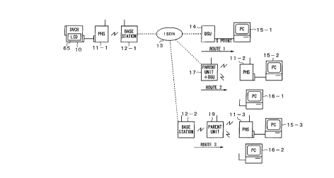
Fig. 1 is a schematic diagram showing an
example of the structure of a picture sending/receiving
system according to an embodiment of the present
invention. In this embodiment, a DVCR 10 digitizes a
picture signal received from a CCD ~not shown),
performs a picture compressing process such as an
orthogonal converting process, records the resultant
signal as video data on a magnetic tape, and displays
the video data on an LCD (Liquid Crystal Display) 65.
In addition, the DVCR 10 outputs video data to a PHS
CA 02221184 1997-11-13
(Personal Handyphone System) 11-1 through IEEE (The
Institute of Electrical and Electronic Engineers) 1394
standard.
The IEEE 1394 standard is a general standard
that supports an isochronous data transmission. Since
the isochronous data transmission ensures that data
transmission is completed in a predetermined time
period, a moving picture and sound can be smoothly
reproduced.
Base stations 12-1, 12-2, and so forth are
disposed in individual service areas. The base
stations 12-1 and 12-2 exchange data as a radio wave
with the PHS 11-1 and a parent unit 19. An ISDN line
13 sends data among the base stations 12-1 and 12-2, a
DSU (Digital Service Unit) 14, and a parent unit 17.
The DSU 14 connects the ISDN line 13 and a
personal computer 15-1. In addition, when the DSU 14
exchanges data between the ISDN line 13 and the
personal computer 15-1, the DSU 14 converts the format
of the data. The personal computers 15-1 to 15-3
perform predetermined processes for received video
data, display the resultant data on their display
units, and record the data on their hard disks or the
like (not shown).
The parent unit 17 has a DSU. The DSU
modulates a carrier corresponding to data received
through the ISDN line 13 and sends the modulated
CA 02221184 1997-11-13
carrier as a radio wave to a PHS 11-2. In addition,
the parent unit 17 converts a radio wave received from
the PHS 11-2 into an electric signal and sends the
resultant signal to the ISDN line 13. A personal
computer 16-1 sends and receives data as a radio wave
to/from the parent unit 17. In addition, the personal
computer 16-1 performs a predetermined process for
received data, displays the resultant data on its
display unit, and records the data on a hard disk or
the like (not shown).
The base station 12-2 modulates a carrier
corresponding to data received through the ISDN line 13
and sends the carrier as a radio wave to a parent unit
19. In addition, the base station 12-2 receives a
radlo wave from the parent unit 19, converts the radio
wave into an electric signal, and sends the electric
signal to the ISDN line 13. The parent unit 19
amplifies the radio wave received from the base station
12-2 and sends the resultant radio wave to a PHS 11-3
or a personal computer 16-2. In addition, the parent
unit 19 receives a radio wave from the PHS 11-3 or the
personal computer 16-2, amplifies the received radio
wave, and sends the resultant radio wave to the base
station 12-2. In this structure, since the parent unit
19 functions as a relaying unit, a radio wave with a
sufficient intensity can be sent and received
regardless of geographic conditions and so forth.
CA 0222ll84 l997-ll-l3
Next, the operation of the embodiment will be
described.
Video data that is output from the DVCR 10 is
input to the PHS 11-1. The PHS 11-1 performs a
predetermined process (that will be described later)
for the input video data, modulates a carrier of 1.9
GHz corresponding to the received signal and sends the
modulated carrier as a radio wave to the base station
12-1. The base station 12-1 receives the radio wave
from the PHS 11-1, converts the received radio wave
into an electric signal, and sends the electric signal
to the ISDN line 13.
On route 1, a signal (data) is sent to the
DSU 14 through the ISDN line 13. The DSU 14 separates
a multiplexed signal of a send signal and a receive
signal received through the ISDN line 13 into two send
signals and two receive signals at S/T point (or
referred to as I interface) and supplies these
separated signals to the personal computer 15-1. In
addition, the DSU 14 performs a process for converting
transmission rates of signals from 64 kbps to 32 kbps.
The DSU 14 sends the resultant signals to the personal
computer 15-1. The personal computer 15-1 performs a
predetermined process for the converted signals and
displays the resultant signals as a picture on the
display unit. In addition, the personal computer 15-1
can send data.
12
CA 02221184 1997-11-13
On route 2, the parent unit 17 performs the
above-described converting process (performed by the
DSU 14 on the route 1) for data received through the
ISDN line 13, converts the resultant signals into a
radio wave corresponding to a PHS format, and sends the
radio wave. The PHS 11-2 receives the radio wave from
the parent unit 17, performs the predetermined process
for the radio wave, and sends the resultant signal to
the personal computer 15-2 through the IEEE 1394
interface. The personal computer 15-2 reads a signal
from the IEEE 1394 interface through an ISA (Industry
Standard Architecture) bus or a PCI (Peripheral
Component Interconnect) bus, performs the predetermined
process for the resultant signal, displays the
resultant signal as a picture on the display unit, and
records the signal on a hard disk or the like (not
shown). In addition, the personal computer 15-2 can
send picture data on the reverse route.
Since the personal computer 16-1 has a
function for receiving a radio wave corresponding to
the PHS format, the personal computer 16-1 receives a
radio wave from the parent unit 17, performs the
predetermined process for the received radio wave,
displays the resultant signal as a picture on the
display unit, and records the signal on a hard disk or
the like (not shown).
On route 3, the base station 12-2 converts
CA 02221184 1997-11-13
data received through the ISDN line 13 into a radio
wave corresponding to the PHS format and sends the
radio wave to the parent unit 19. The parent unit 19
receives the radio wave from the base station 12-2,
amplifies the radio wave, and sends the amplified radio
wave to the PHS 11-3. The PHS 11-3 receives the radio
wave from the parent unit 19, performs the
predetermined process for the radio wave, and sends the
resultant signal to the personal computer 15-3. As
with the routes 1 and 2, the personal computer 15-3
performs the predetermined process for the input
signal, displays the resultant signal on the display
unit, and records the signal on a hard disk or the like
(not shown).
As with the personal computer 16-1, the
personal computer 16-2 has a function for receiving a
radio wave corresponding to the PHS format. Thus, the
personal computer 16-2 receives a radio wave from the
parent unit 19, performs the predetermined process for
the radio wave, displays the resultant signal as a
picture on the display unit, and records the signal on
a hard disk or the like (not shown).
In each of the personal computers 15-1 to 15-
3, a DVCR decoding IC or software performs a
decompressing process for the received video data (that
has been picture-compressed corresponding to DVCR
system). The resultant picture is displayed on the
14
CA 02221184 1997-11-13
display unit and recorded on a hard disk or the like
(not shown). In addition, a picture and so forth
recorded on the hard disk or the like can be compressed
by a DVCR encoding IC or software and then output.
As described above, each of the personal
computers 16-1 and 16-2 sends and receives a radio wave
corresponding to the PHS format. Moreover, in each of
the personal computers 16-1 and 16-2, the DVCR decoding
IC and DVCR encoding IC or software performs the
picture compressing/decompressing process.
Fig. 2 is a block diagram showing an example
of the structure of the DVCR 1 shown in Fig. 1. The
DVCR 10 comprises an A/D converter 50, a block
segmenting/shuffling portion 51, a memory 52, a
DCT/IDCT calculating portion 53, a
quantizing/dequantizing portion 54, a fixed length data
forming portion 55, a shuffling/deshuffling portion 56,
a memory 57, an ECC portion 58, a modulating portion
59, a recording/reproducing (playback) amplifier
portion (R/P AMP) 60, a packet forming portion 61, a
driver 62, a connector 63, a D/A converter 64, and an
LCD 65.
The A/D converter 50 converts a video signal
(composed of luminance signal, red color difference
signal, and blue color difference signal) that is
output from a CCD (not shown) into digital data. In
this case, the ratio of the sampling frequency of the
CA 02221184 1997-11-13
luminance signal of the A/D converter 50 and the
sampling frequency of the red color difference signal
or the blue color difference signal is 4 to 1. The A/D
converter 50 supplies a digitized video signal
(hereinafter referred to as video data) to the block
segmenting/shuffling portion 51. The block
segmenting/shuffling portion 51 performs a block
segmenting process and a shuffling process for the
video data.
In other words, in the block segmenting
process of the block segmenting/shuffling portion 51,
video data (composed of luminance data Y, red color
difference data CR, and blue color data CB) of each
frame supplied from the A/D converter 50 is divided
into blocks each of which is composed of 8 x 8 pixels.
These blocks are referred to as DCT (Discrete Cosin
Transform) blocks.
In this case, since the sampling frequency of
the luminance signal of the A/D converter 50 is
different from the sampling frequency of the color
difference signal thereof, four blocks of the luminance
data Y, one block of the color difference data CR, and
one block of the color difference data CB are present
at the same position (area) on the screen. For
example, in the case of 525/60 system, as shown in Fig.
3, in the horizontal direction of one frame (left and
right directions of Fig. 3), 90 blocks of luminance
16
CA 02221184 1997-11-13
data Y, 22.5 blocks of color difference data CR, and
22.5 blocks of color difference data CB are placed. In
the vertical direction (upper and lower directions of
Fig. 3), 60 blocks of luminance data Y, 60 blocks of
color difference data CR, and 60 blocks of color
difference data CB are placed.
A total of six blocks (four blocks of
luminance data Y (Y0 to Y3), one block of color
difference data CR, and one block of color difference
data CB) are treated as one process unit. These 6
blocks are referred to as a macro block (MB). Figs. 4A
and 4B show the structures of macro blocks of the
525/60 system. Fig. 4B shows the structure of a macro
block at an edge portion of the screen of which the
number of blocks of each of the color difference data
CR and CB is 0.5 blocks. Fig. 4A shows the structure
of a macro block at other portions of the screen.
In the shuffling process performed by the
block segmenting/shuffling portion 51, five macro
blocks as a fixed length data forming unit are
collected from one frame of picture data stored in the
memory 52 corresponding to a predetermined rule. With
the process for collecting five macro blocks
corresponding to the predetermined rule, picture data
is shuffled.
The five macro blocks are referred to as a
buffering unit (BU). As described above, by shuffling
CA 02221184 1997-11-13
five macro blocks, information amount of each buffering
unit is equalized (averaged). Thus, the distortion due
to data compression can be equalized on the screen.
In the 525/60 system, the shuffling process
is performed in the following manner.
As shown in Fig. 5, one screen is
horizontally divided into five portions corresponding
to the number of macro blocks in a video segment (that
will be described later). In addition, the screen is
vertically divided (into ten portions) corresponding to
the number of tracks of the magnetic tape on which one
frame of data is recorded. One block divided in such a
manner is referred to as a super bock. Each super
block is composed of 27 macro blocks.
Super blocks are selected from individual
vertical rows. First of all, macro blocks (No. 0)
contained in individual super blocks are collected and
thereby a first video segment (MB1 to MB5) are
structured. Next, macro blocks (No. 1) are collected
from the same super blocks and thereby a second video
segment is structured. The same process is repeated.
After all macro blocks are collected from the five
super blocks, the next five super blocks are processed.
In other words, the next super blocks are selected in
the order of arrows a to e shown in Fig. 5.
Video segments that have been block segmented
and shuffled by the block segmenting/shuffling portion
18
CA 02221184 1997-11-13
51 shown in Fig. 5 are supplied to the DCT/IDCT
calculating portion 53. The DCT/IDCT calculating
portion 53 performs a DCT calculating process and a
variable length code encoding process for the input
video segments. The quantizing/dequantizing portion 54
selects a quantizing step with a maximum number of bits
in the range that the number of bits (encoded amount)
of data that has been variable-length-code encoded does
not exceed the number of bits (number of target bits)
of the video segments and quantizes the video segments
with the selected quantizing step. The
quantizing/dequantizing portion 54 zig-zag scans
coefficients of individual quantized blocks starting
from DC component corresponding to modified two-
dimensional Huffman encoding process and assigns code
as a set of run length with coefficient "0" and a non-
zero coefficient.
Output data of the quantizing/dequantizing
portion 54 is supplied to the fixed length data forming
portion 55. The fixed length data forming portion 55
packs data of individual video segments as five sync
blocks (SB) (that will be described later).
Sync blocks are separated small areas on
tracks of the magnetic tape. In other words, a video
data record area on each track of the magnetic tape is
divided into small areas referred to as sync blocks.
The number of sync blocks on one block is 135. As
CA 02221184 1997-11-13
described above, in the 525/60 system, as shown in Fig.
6, one frame of video data is divided into 10 portions
(tracks 0 to 9) and recorded thereon. Thus, the number
of sync blocks per frame is 1350 that is equal to the
number of macro blocks per frame.
Fig. 7 shows the structure of principal
portions of a sync block. The length of each sync
block is 90 bytes. Sync pattern data is placed at
bytes 0 and 1 (not shown). Likewise, an error
correction parity is placed at bytes 82 to 89 (not
shown). A track pair number is placed at low order
four bits (including LSB (Least Significant Bit)) of
byte 2. As shown in Fig. 8, track numbers (0 to 9) are
represented as four-bit binary numbers. A sequence
number is placed at high order four bits (MSB (Most
Significant Bit) of byte 2.
A sync number that represents the position in
135 sync blocks of one track is placed at byte 3. As
shown in Fig. 9, the sync number is represented as an
eight-bit binary number.
A parity is placed at byte 4. A quantizing
table number (QNO) that represents information of a
quantizing step is placed at low-order four bits of
byte 5. Information (STA) that represents whether or
not the macro block has an error is placed at high-
order four bits of byte 5. The quantizing table number
is used to perform the dequantizing process.
CA 02221184 1997-11-13
Data of luminance blocks Y0 to Y3 composing
the macro block is placed at bytes 6 to 19, bytes 20 to
33, bytes 34 to 47, and bytes 48 to 61, respectively.
Data of color difference blocks CR and CB that compose
the macro block is placed at bytes 62 to 71 and bytes
72 to 81, respectively. When data of a particular
block is not placed in the predetermined area, the data
is placed in a blank area of another block of the same
sync block. When data of a particular macro block is
not placed in an area at bytes 6 to 81, the data is
placed in a blank area of another sync block of the
five sync blocks.
As shown in Fig. 7, the luminance blocks Y0
and Y3 or the color difference blocks CR and CB that
compose the macro block contain a DC component of data
and an AC component of data. The DC component of data
is placed at the first byte (eight bits) of each block
and the MSB (one bit) of the second byte. Thus, the DC
component is composed of nine bits. Flags c0, cl, and
mO are placed at Bits 5 to 7 of byte 2, respectively.
AC components are placed in other areas. "0110" that
represents EOB (End of Block) is placed at the end of
each AC component. An enlarged macro block shown in
Fig. 7 does not contain an AC component. In this case,
"0110" that represents EOB is placed at bits 1 to 4 of
the second byte.
Output data of the fixed length data forming
CA 02221184 1997-11-13
portion 55 is supplied to the packet forming portion
61. In addition, the output data of the fixed length
data forming portion 55 is supplied to the
shuffling/deshuffling portion 56. The packet forming
portion 61 performs a packet forming process for
compressed video data (at bytes 2 to 81 of each sync
block) and supplies the resultant packet data to the
driver 62. The driver 62 converts the packet data into
serial data corresponding to the format of the IEEE
1394 standard and outputs the resultant serial data
through the connector 63.
The shuffling/deshuffling portion 56 writes
data of each video segment of which five sync blocks
have been packed (namely, shuffled data) to the memory
57 in the order shown in Fig. 5 so as to obtain the
original picture data. The shuffling/deshuffling
portion 56 reads sync block data of each frame from the
memory 57 so that the sync block data is recorded in
the order of track 0 to track 9 of the magnetic tape
and supplies the resultant data to the ECC portion 58.
The ECC portion 58 adds an error correction
parity to the data received from the
shuffling/deshuffling portion 56 and supplies the
resultant data to the modulating portion 59. The
modulating portion 59 performs a digital modulating
process for the sync block data received from the ECC
portion 59 and supplies the resultant data to the
CA 02221184 1997-11-13
recording/reproducing (playback) amplifier portion (R/P
AMP) 60. The recording/reproducing amplifier portion
60 amplifies the signal received from the modulating
portion 59 with a predetermined amplitude, supplies the
resultant signal to a rotting magnetic head (not
shown), and records the signal on the magnetic tape.
Thus, a process for recording a picture
signal received from a CCD to a magnetic tape and a
process for outputting a picture signal from the
connector 63 have been completed. Next, a process for
displaying data that is received from the connector 63
or data recorded on a magnetic tape on the LCD 65 will
be described in brief.
A picture signal reproduced by the rotating
magnetic head is amplified by the recording/reproducing
amplifier portion 60 at the predetermined amplitude.
The resultant signal is supplied to the modulating
portion 59. The modulating portion 59 performs a
digital demodulating process for the amplified signal.
The resultant data is supplied to the ECC portion 58.
The ECC portion 58 performs an error correcting process
for the demodulated data corresponding to the parity.
The resultant signal is supplied to the
shuffling/deshuffling portion 56. The
shuffling/deshuffling portion 56 performs a shuffling
process for the error-corrected data (see Fig. 5) and
supplies the resultant data to the fixed length data
23
CA 02221184 1997-11-13
forming portion 55.
On the other hand, serial data that is
received from an external unit through the connector 63
is supplied to the driver 62. The driver 62 converts
the serial data into parallel data. The parallel data
is supplied to the packet forming portion 61. The
packet forming portion 61 depacks the parallel data
(that has been packed) and outputs the resultant data.
The output data of the shuffling/deshuffling
portion 56 or the output data of the packet forming
portion 61 is supplied to the fixed length data forming
portion 55. The fixed length data forming portion 55
performs a depacking process for the data that has been
packed and supplies the resultant data to the
quantizing/dequantizing portion 54. The
quantizing/dequantizing portion 54 performs a variable-
length-code dequantizing process and a dequantizing
process for the depacked data and supplies the
resultant data to a DCT/IDCT calculating portion 53.
The DCT/IDCT calculating portion 53 performs
an IDCT calculation for the data received from the
quantizing/dequantizing portion 54 and supplies the
resultant data to the block segmenting/shuffling
portion 51. The block segmenting/shuffling portion 51
performs a deshuffling process and a block desegmenting
process for the data received from the DCT/IDCT
calculating portion 53 and outputs the resultant data
24
CA 02221184 1997-11-13
to the D/A converter 64. The D/A converter 64 converts
the received digital data to the original analog signal
and supplies the resultant signal as a video signal to
the LCD 65. The LCD 65 displays the video signal as a
picture.
Next, with reference to Figs. 10 and 11, an
example of the structure of the PHS 11 (11-1 to 11-3)
shown in Fig. 1 will be described in detail. The PHS
11 is composed of a PHS sending/receiving portion 100
shown in Fig. 10 and a DVCR-PHS interface portion 110
shown in Fig. 11.
The PHS sending/receiving portion 100 shown
in Fig. 10 is composed of an antenna 90, a switch 91, a
receiving portion 92 (receiving means or receiving
step), a communication controlling portion 93, a data
transmission controlling portion 94, a digital
interface (I/F) portion 95, a synthesizer 96, and a
sending portion (sending means, sending step, first
sending means, first sending step, second sending
means, or second sending step).
The antenna 90 sends a radio wave to the base
station 12-1 (or the parent station 17 or 19). In
addition, the antenna 90 receives a radio wave from the
base station 12-2. A switch position of the switch 91
is changed by the communication controlling portion 93
depending on whether or not a radio wave is sent or
received. The receiving portion 92 converts the radio
CA 02221184 1997-11-13
wave received through the switch 91 into an electric
signal and supplies the electric signal to the
communication controlling portion 93. The
communication controlling portion 93 extracts a frame
from the signal received from the receiving portion 92
and supplies the frame to the data transmission
controlling portion 94. The data transmission
controlling portion 94 checks an error of the signal
received from the communication controlling portion 93.
When the signal does not have an error, the data
transmission controlling portion 94 supplies the signal
received from the communication controlling portion 93
to the DVCR-PHS interface portion 110 (see Fig. 11)
through the digital interface portion 95. In contrast,
when the signal received from the communication
controlling portion 93 has an error, the data
transmission controlling portion 94 requests the sender
side to re-send the signal and receives the signal
therefrom.
Fig. 12 is a schematic diagram showing an
example of the format of data that is output from the
digital interface portion 95. In this example, the
structure of data corresponding to PIAF (PHS Internet
Access Forum Standard) format is shown.
In the PIAF format, one frame has a fixed
length of 640 bits. Bits 1 to 4 represent a frame
identification number (FI). The next six bits
CA 02221184 1997-11-13
represent a frame number (FFI). The next six bits
represent a request frame number (FBI). These three
types of information are referred to as ARQ (Automatic
Request for Repeat) control information.
The next one bit is a frame continuation
identification bit that is used to determine whether or
not the current frame is continued from the previous
frame. The next seven bits represent the number of
bytes of meaningful bits stored in the user data area.
The next 584 bytes represent user data.
Eight bytes of the user data represent a modulo
identifier that is used to manage the modulo of the
frame. The last 32 bytes (CRC 32) are used to detect
an error of the frame.
Referring to Fig. 10, an output signal of the
DVCR-PHS interface portion 110 is supplied to the
digital interface portion 95. The digital interface
portion 95 converts the signal received from the
digital I/F portion 95 into an analog signal. The
analog signal is supplied to the data transmission
controlling portion 94. The data transmission
controlling portion 94 converts the analog signal
received from the digital interface portion 95 into a
signal corresponding to a PHS communication protocol.
The resultant signal is supplied to the communication
controlling portion 93. The communication controlling
portion 93 converts the signal received from the data
CA 02221184 1997-11-13
transmission controlling portion 94 into a signal
corresponding to the PHS format and supplies the
resultant signal to the sending portion 97.
The sending portion 97 modulates a carrier of
1.9 GHz received from the synthesizer 96 corresponding
to the signal received from the communication
controlling portion 93 and outputs the resultant signal
as a radio wave from the antenna 90 through the switch
91 .
Fig. 11 is a block diagram showing an example
of the structure of the DVCR-PHS interface portion 110
that connects the PHS 11-1 and the DVCR 10 (PHS 11-2 or
11-3 and the personal computer 15-2 or 15-3).
The DVCR-PHS interface portion 110 is
composed of a connector 111, a driver 112 (outputting
means or outputting step), a packet forming portion
113, an encoding portion 114 (reading means, reading
step, adding means, adding step, extracting means,
extracting step, separating and extracting means, or
separating and extracting step), a frame memory 115
(storing means or storing step), a data processing
portion 116, and an ID number detecting portion 117
that is disposed in the data processing portion 116.
The connector 111 is a connector
corresponding to the IEEE 1394 standard. The connector
111 is connected to the DVCR 10 with a cable. The
driver 112 converts serial data received from the
28
CA 02221184 1997-11-13
connector 111 into parallel data. In addition, the
driver 112 converts parallel data received from the
packet forming portion 113 into serial data. The
packet forming portion 113 depacks the parallel data
received from the driver 112. In addition, the packet
forming portion 113 packs the parallel data received
from the encoding portion 114 as packet data and
supplies the packet data to the driver 112. The packet
forming portion 113 detects a frame pulse signal from
the data received from the driver 112 and supplies the
frame pulse signal to the encoding portion 114.
The encoding portion 114 writes one frame of
data to the frame memory 115 corresponding to the frame
pulse signal received from the packet forming portion
113 and executes a header encoding process for sending
information associated with picture data. The encoding
portion 114 reads one frame of data that has been
received from the PHS 11-1 and written to the frame
memory 115 at intervals of 1/30 seconds that are frame
intervals and supplies the data as video data to the
packet forming portion 113.
The data processing portion 116 controls the
packet forming portion 113, the encoding portion 114,
and the frame memory 115. The ID number detecting
portion 117 of the data processing portion 116 detects
an ID number from the data received from the PHS 11-1
and supplies the ID number to the encoding portion 114.
29
CA 02221184 1997-11-13
Next, with reference to Figs. 10 and 11, the
process for sending picture data from the DVCR 10
through the PHS 11-1 will be described.
Video data received from the DVCR 10 shown in
Fig. 2 is sent to the DVCR-PHS interface portion 110
through the connector 111. The driver 112 converts the
received video data into parallel data and supplies the
resultant data to the packet forming portion 113. The
packet forming portion 113 depacks packet video data
and supplies the resultant data to the encoding portion
114. The encoding portion 114 performs a header
encoding process for information associated with the
video data and successively writes video data to a
predetermined area of the frame memory 115.
The data processing portion 116 successively
reads only DC components from one frame of picture data
stored in the frame memory 115 corresponding to the
transmission rate of the PHS 11-1 and outputs the DC
components. Thereafter, the data processing portion
116 reads AC components from one frame of picture data
stored in the frame memory 115 and outputs the AC
components.
Output data of the DVCR-PHS interface portion
110 is supplied to the digital interface portion 95 of
the PHS 11 shown in Fig. 10. The digital interface
portion 95 converts the received digital data into an
analog signal and supplies the analog signal to the
CA 02221184 1997-11-13
data transmission controlling portion 94. The data
transmission controlling portion 94 converts the analog
signal received from the digital interface portion 95
into a signal corresponding to the PHS communication
protocol. The communication controlling portion 93
converts the signal received from the data transmission
controlling portion 94 into a signal corresponding to
the PHS format and supplies the resultant signal to the
sending portion 97.
The sending portion 97 modulates a carrier of
1.9 GHz received from the synthesizer 96 corresponding
to the signal received from the communication
controlling portion 93 and outputs the resultant signal
as a radio wave from the antenna 90 through the switch
91.
The radio wave is received by the base
station 12-1 (or parent unit 17 or 19). After the
radio wave is processed by the base station 12-1, the
resultant signal is sent to a predetermined terminal
through the ISDN line 13.
Next, the process for receiving data through
the ISDN line 13 and displaylng the received data on
the display unit will be described. The routes 2 and 3
of which data received through the ISDN line 13 is
converted into a radio wave will be described.
On the route 2, picture data received through
the ISDN line 13 is supplied to the DSU of the parent
CA 02221184 1997-11-13
unit 17. The DSU converts the received picture data
into predetermined data, converts the resultant data
into a radio wave corresponding to the PHS format, and
sends the radio wave.
Since the structure of the PHS 11-2 is the
same as the structure of the PHS 11-1 shown in Figs. 10
and 11, with reference to Figs. 10 and 11, the
operation of the PHS 11-2 will be described.
A radio wave received by the antenna 90 shown
in Fig. 10 is supplied to the switch 91. The switch
position of the switch 91 is changed by the
communication controlling portion 93. At this point,
the switch 91 is connected to the position of the
receiving portion 92. Thus, the radio wave received
from the switch 91 is supplied to the receiving portion
92. The receiving portion 92 converts the received
radio wave into an electric signal corresponding
thereto and supplies the electric signal to the
communication controlling portion 93. The
communication controlling portion 93 extracts a frame
from the electric signal received from the receiving
portion 92 and supplies the frame to the data
transmission controlling portion 94. The data
transmission controlling portion 94 checks an error of
the signal received from the communication controlling
portion 93. When the signal does not have an error,
the data transmission controlling portion 94 sends the
CA 02221184 1997-11-13
signal to the DVCR-PHS interface portion 110 (see Fig.
11) through the digital interface portion 95.
When the signal has an error, the data
transmission controlling portion 94 requests the sender
side to re-send the signal and receives the signal
therefrom.
Data that is sent to the DVCR-PHS interface
portion 110 shown in Fig. 11 is successively stored in
the frame memory 115. As described above, the picture
data is sent in the order of DC components and AC
components. Thus, the data is stored in the frame
memory in such an order. At this point, as shown in
Fig. 7, the DC components are DC0 to DC5 at first byte
of the individual macro blocks (Y0 to Y3 or CR and CB).
Thus, the amount of information of one frame is around
864 kbits. The DC components are stored in the same
order as macro blocks of the shuffling process shown in
Fig. 5. In other words, macro block data is stored in
the frame memory 115 in the same order as the reading
process thereof.
When the data processing portion 116 receives
a sync block, it outputs the frame pulse signal to the
ID number detecting portion 117. When the ID number
detecting portion 117 receives the frame pulse signal,
the ID number detecting portion 117 detects an ID
(track pair number and sync number (see Fig. 7)) from
the data received from the PHS 11 and supplies the
CA 02221184 1997-11-13
detected ID to the encoding portion 114.
The encoding portion 114 reads data stored in
the frame memory 115 at intervals of 1/30 seconds that
are frame intervals of the video signal and sends the
read data as video data to the packet forming portion
113.
Data received from the digital interface
portion 95 of the PHS sending/receiving portion 100 is
successively stored in the frame memory 115 at 32
kbits/s that is the information transmission rate of
the ISDN line. On the other hand, since the encoding
portion 114 reads one frame of data at intervals of
1/30 seconds, before all data is stored in the frame
memory 115, the data is read as video data.
With reference to the ID (of a sync block
stored in the frame memory 115) received from the ID
number detecting portion 117, the encoding portion 114
reads a buffering unit (composed of five sync blocks)
of picture data and outputs the buffering unit as it
is. When the picture data is a fragment of a buffering
unit (namely, the entire sync block has not been
stored), the encoding portion 114 outputs a gray code
of which all DC components are "0" and 'l0110" that
represents EOB is placed at bits 1 (LSB) to
bit 4 of the second byte. Fig. 13A shows a gray code
corresponding to the luminance blocks Y0 to Y3. Fig.
13B shows a gray code corresponding to the color
34
CA 02221184 1997-11-13
difference blocks CR and CB.
When a new frame data is received, the
encoding portion 114 erases the ID of the former frame.
Thus, the aforementioned process is repeated frame by
frame.
Video data received from the encoding portion
114 is supplied to the packet forming portion 113. The
packet forming portion 113 packs the video data as
packet data with a predetermined length and supplies
the packet data to the driver 112. The driver 112
converts the packet data into serial data corresponding
to the IEEE 1394 standard and outputs the serial data
through the connector 111.
The video data is supplied to the personal
computer 15-2 shown in Fig. 1. The personal computer
15-2 converts the data received from the DVCR-PHS
interface portion 110 into the original picture data
with the DVCR decoding IC or the software and displays
the resultant data on the display unit.
In this case, video data that is supplied to
the personal computer 15-2 is displayed in the
following process.
When the PHS sending/receiving portion 100
shown in Fig. 10 starts receiving a new frame of
picture data, the encoding portion 114 of the DVCR-PHS
interface portion 110 shown in Fig. 11 erases the ID of
the previous frame. Thus, video data composed of gray
CA 02221184 1997-11-13
data shown in Fig. 13 is output. Consequently, the
entire screen of the display unit of the personal
computer becomes gray.
When the PHS sending/receiving portion 100
starts receiving DC components, they are stored in the
frame memory 115. The video data that is output from
the DVCR-PHS interface portion 110 is composed of DC
components of an area that has been completely received
and gray data of an area that has not been completely
received. Thus, as DC components are received, a
picture of the DC components is gradually displayed on
the gray screen. It takes around one second to receive
the DC components. Around one second after frame data
is received, the picture of the DC components is
displayed.
Fig. 14 is a schematic diagram showing
picture data composed of only DC components displayed.
With the DC components being displayed, a rough contour
of the picture can be recognized.
Thereafter, the PHS sending/receiving portion
100 receives AC components of the picture data. When
the AC components are received and supplied to the
DVCR-PHS interface portion 100, the picture of the area
that has been completely received becomes the same as
the original picture (stored on the sender side).
Thus, as the AC components are received, the original
picture is gradually displayed. It takes around 12.5
CA 02221184 1997-11-13
seconds to receive the complete AC components.
Fig. 15 shows an example of an original
picture (shown in Fig. 14) displayed in the
conventional method (of which both the DC component and
the AC component are displayed at the same time). In
this case, since the original picture (composed of DC
components and AC components) is received and
reproduced as super blocks, the picture is partially
displayed as shown in Fig. 15. It takes around 13.5
seconds to display one frame of picture. In other
words, according to the conventional method, it takes a
longer time for the user to recognize a picture that is
displayed.
As described above, according to the present
invention, with the DC components received from the
sender side, a rough contour of the picture can be
recognized. Thus, the user can recognize the received
picture in a relatively short time. In addition, since
the encoding portion 114 processes a buffering unit of
data stored in the frame memory 115 at a time, when the
obtained video data is supplied to the DVCR 10 or the
like, the picture can be decoded free from an error.
The personal computer 15-1 includes the DVCR-
PHS interface portion 110 shown in Fig. 11, the DVCR
encoding IC, and the DVCR decoding IC. The data
received from the DSU 14 is supplied to the DVCR-PHS
interface portion 110. The DVCR-PHS interface portion
CA 02221184 1997-11-13
110 converts the data received from the DSU 14 into
video data. The DVCR decoding IC converts the data
received from the DSU 14 into a picture signal. The
picture signal is displayed on the display unit and
also recorded on a hard disk or the like (not shown).
In addition, a picture signal recorded on a hard disk
or the like (not shown) is sent to the DVCR encoding
IC. The DVCR encoding IC encodes the picture signal.
The resultant signal is sent to the DVCR-PHS interface
portion 110. The DVCR-PHS interface portion 110
converts the encoded signal into predetermined data.
Each of the personal computers 16-1 and 16-2
includes the PHS sending/receiving portion 100 shown in
Fig. 10, the DVCR-PHS interface portion 110 shown in
Fig. 11, the DVCR encoding IC, and the DVCR decoding
IC. Each of the personal computers 16-1 and 16-2
receives a radio wave from the parent unit 17 or 19,
reproduces the picture in the same operation as the
personal computer 15-1, converts a picture signal
recorded on a hard disk or the like (not shown) into a
radio wave, and sends the radio wave.
In the above-described embodiment, the
picture signal is sent in the order of DC components
and AC components. However, only DC components of the
picture signal may be sent. Next, such a case will be
described with reference to the embodiment shown in
Figs. 10 and 11.
38
CA 022211X4 1997-11-13
Video data that is received from the DVCR 10
(or personal computer 15-2 or 15-3) through the
connector 111 is supplied to the driver 112. The
driver 112 converts the video data into parallel data
and supplies the parallel data to the packet forming
portion 113. The packet forming portion 113 depacks
the packet video data and supplies the resultant data
to the encoding portion 114.
The encoding portion 114 stores data "0110"
that represents ~OB at bits 1 to 4 of the second byte
(the first four bits of the area that stores an AC
component) of a macro block contained in a sync block
that composes video data received from the packet
forming portion 113. Thus, the data "0110" represents
that the macro block contains only a DC component. DC
components of the picture signal received from the
encoding portion 114 are successively stored in the
frame memory 115. The DC components stored in the
frame memory 115 are read in the order as shown in Fig.
5 and sent to the PHS sending/receiving portion 100.
The PHS sending/receiving portion 100 modulates a
carrier corresponding to the received data and sends
the modulated carrier as a radio wave from the antenna
90 .
The radio wave sent from the PHS
sending/receiving portion 100 is received by the base
station 12-1 or 12-2 or the parent unit 17. The base
39
CA 02221184 1997-11-13
station 12-1 or 12-2 or the parent unit 17 converts the
radio wave into an electric signal and sends the
electric signal to the ISDN line 13. Data sent through
the ISDN line 13 is received by a predetermined
terminal unit. The predetermined terminal unit decodes
the received data into an original picture signal. The
original picture signal is displayed on the display
unit or the like.
For example, when the personal computer 15-2
is selected as a terminal unit, the data received
through the ISDN line 13 is sent to the parent unit 17.
The parent unit 17 converts the received data into a
radio wave and sends the radio wave. The PHS
sending/receiving portion 100 receives the radio wave
from the parent unit 17, performs the above-described
process for the radio wave, and sends the resultant
signal to the DVCR-PHS interface portion 110 shown in
Fig. 11. The DVCR-PHS interface portion 110
successively stores the received data in the
predetermined area of the frame memory 115. The
encoding portion 114 reads the data stored in the frame
memory 115 at intervals of 1/30 seconds and outputs the
read data as video data through the packet forming
portion 113 and the driver portion 112.
Thus, a gray picture composed of gray data is
displayed on the display unit of the personal computer
15-2. As DC components are received, a picture as
CA 02221184 1997-11-13
shown in Fig. 14 is gradually displayed.
According to the above-described structure,
only DC components can be extracted from the video data
(moving picture) received from the DVCR 10 (or the
personal computer 15-2 or 15-3) and the extracted DC
components can be supplied to the receiver side through
the ISDN line 13. Since it takes around one second to
send the DC components for one frame, new pictures are
displayed every one second on the receiver side. Thus,
pictures are displayed as with a semi-moving picture.
In the embodiment, a total of nine bits of
the first byte and bit 8 of the second byte of each
macro block are sent as DC components. However, only
eight bits of the first byte may be sent. Thus, since
the amount of information per frame can be reduced, the
transmission rate can be increased. In addition, since
digital data is mainly processed in a unit of eight
bits, a conventional signal processing portion of the
receiving apparatus can be used. Consequently, the
cost of the apparatus can be reduced. Moreover, the
apparatus can be simply designed.
When the number of bits of information of a
picture is decreased by one, the amount of information
to ~e sent is decreased. However, the deterioration of
the picture quality is small.
Fig. 16 is a block diagram showing an example
of the structure of a public telephone line type
41
CA 02221184 1997-11-13
sending/receiving apparatus using a public (analog)
telephone line. The public telephone line type
sending/receiving apparatus sends and receives picture
data.
In Fig. 16, similar portions to those in Fig.
10 are denoted by similar reference numerals and
description thereof is omitted. The structure shown in
Fig. 16 is the same as the structure shown in Fig. 10
except that the antenna 90, the switch 91, the
receiving portion 92, the data transmission controlling
portion 94, the synthesizer 96, and the sending portion
are removed and that a modem portion 131 is newly
added. The modem portion 131 is connected to a public
telephone line 150.
The modem portion 131 modulates data received
from the communication controlling portion 93 in a
signal format corresponding to the public telephone
line 150. In addition, the modem portion 131
demodulates data received through the public telephone
line 150 and supplies the demodulated data to the
communication controlling portion 93.
Next, the sending operation and the receiving
operation of the embodiment will be described in brief.
The DVCR-PHS interface portion 110
successively extracts DC components and AC components
from each frame of video data received from the DVCR 10
or the personal computer 15-2 or 15-3 and sends the DC
42
CA 02221184 1997-11-13
components and the AC components to the digital
interface portion 95 of the public telephone line type
sending/receiving apparatus 130. The digital interface
portion 95 converts serial data received from the DVCR-
PHS interface portion 110 into parallel data and
supplies the parallel data to the communication
controlling portion 93. The communication controlling
portion 93 converts the data received from the digital
interface portion 95 corresponding to the protocol of
the public telephone line 150.
The modem portion 131 converts data received
from the communication controlling portion 93 into an
analog signal corresponding to the public telephone
line 150 and sends the resultant signal to the public
telephone line 150.
In other words, the video data that is
received from the DVCR 10 iS sent to the DVCR-PHS
interface portion 110. The DVCR-PHS interface portion
110 successively extracts DC components and AC
components from each frame and sends the DC components
and the AC components to the public telephone line type
sending/receiving apparatus 130. The public telephone
line type sending/receiving apparatus 130 converts data
recelved from the DVCR-PHS interface portion 110 into
an analog signal in the format corresponding to the
public telephone line 150 and sends the resultant
signal to the public telephone line 150.
43
CA 02221184 1997-11-13
Next, the receiving operation of the
embodiment will be described.
Data received through the public telephone
line 150 is sent to the modem portion 131. The modem
portion 131 demodulates the received data into the
original digital signal. The communication controlling
portion 93 extracts a frame from the data received from
the modem portion 131 and supplies the frame to the
digital interface portion 95. The digital interface
portion 95 converts the parallel data received from the
communication controlling portion 93 into serial data
and supplies the serial data to the DVCR-PHS interface
portion 110.
As described above, the DVCR-PHS interface
portion 110 successively writes the received data to
the frame memory 115. In addition, the DVCR-PHS
interface portion 110 converts data stored in the frame
memory 115 into video data, performs a packet forming
process for the video data, and supplies the packet
data to the DVCR 10 (or the personal computer 15-2 ro
15-3). The DVCR 10 displays the input video signal on
the LCD 65. In addition, the DVCR 10 records the
received video signal on a magnetic tape.
In the above-described structure, video data
that is received from the DVCR 10 or the personal
computer 15-2 or 15-3 is extracted in the order of DC
components and AC components. The extracted DC
44
CA 02221184 1997-11-13
components and AC components are sent through the
public telephone line 150. In addition, data received
through the public telephone line 150 is converted into
video data and supplied to the DVCR 10 or the personal
computer 15-2 or 15-3. Thus, the video data is
displayed as a picture. At this point, since the DC
components are sent before the AC components, a rough
contour of the received picture can be quickly
recognized on the receiver side. Thus, the user can
know whether or not the received picture is a desired
picture.
In the above-described embodiment, after DC
components of the video data are sent, AC components
are sent. However, only the DC components may be sent.
In the above-described embodiment, data that
is send and received to/from the digital interface
portion 95 (see Figs. 10 and 16) corresponds to the
PIAF standard. However, it should be noted that other
than the PIAF standard can be used.
Fig. 17 shows an example of another format of
data that is received and sent to/from the digital
interface portion 95. In Fig. 17, the format
corresponding to the HDLC (High-level Data Link
Control) is shown. As shown in Fig. 17A, the first
eight bits of each frame represent data of a flag
sequence. The next eight bits represent an address
field. The next eight bits (or 16 bits) represent a
CA 02221184 1997-11-13
control field. These flag sequence, address field, and
control field are referred to as a control header. The
next information field has any bit length. The
information field stores user data.
The next 16 bits represent a frame
verification sequence. The next eight bits represent a
flag sequence. These frame sequence and flag sequence
are referred to as a control trailer.
When the control field is composed of eight
bits, the format of the field has a structure as shown
in Fig. 17B.
When the control field is composed of 16
bits, the format of the field has a structure as shown
in Fig. 17C.
When data lS sent in the format corresponding
to the HDLC standard, the data can be effectively sent.
In the above-described embodiment, picture
data is sent with (through) the ISDN line 13, the
public telephone line 150, and radio wave as a
transmission medium. However, it should be noted that
the transmission medium is not limited to these.
46