Note: Descriptions are shown in the official language in which they were submitted.
CA 02221200 1997-11-14
DocNo. 10-90 Patent
Reflective Optical Switch
Field of the Invention
This invention relates to optical switches and in particular, to an activation
5 mechanism for an optical switch.
Background of the Invention
In evolving optical communication networks, the need often arises to switch an
optical signal from one path to another, be it along a waveguide or in free space. For
0 example, in a network which consists of a number of communication nodes connected
sequentially to form a ring, it may be required to temporarily remove one or more nodes
from the network. Therefore the optical waveguides, for example in the form of optical
fibres interconnecting the network must be able to "switch" the node(s) from an active
(transmit/receive) state to a passive (bypass) state. Many arrangements exist in the art for
5 providing this type of switching. These arrangements may generally be classified into
two groups: (1) moving beam switches (arrangements which redirect the optical signal
path between stationary waveguides, and (2) moving fibre switches (designs which use
external force to physically change the location of optical fibres entering and exiting the
node). The activation mechanism of the present invention is used with the switches of the
20 former design.
An exemplary optical fibre switch that utilizes a moving mirror to perform the switching
function is disclosed by Levinson in United States patent number 4,580,873 issued April
8, 1986 which is incorporated herein by reference. Although this invention appears to
adequately perform its intended function, it is believed too costly and somewhat complex.
Another switch of the former design is disclosed by Benzoni in United States Patent
5,042,889 and assigned to AT&T Bell Laboratories and issued in 1991. Benzoni's
invention relates to an activation mechanism for moving a reflective element in or out of
the path of a beam of light, to allow light to be either transmitted in a first position or
reflected in a second position. Although Benzoni' s design may perform its intended
30 function, there is a need for an inexpensive optical switch that will allow light to be
transmitted to one of a plurality of different positions. For example, Levinson's matrix
CA 02221200 1997-11-14
Doc No. 10-90 Patent
switch which provides the required functionality of allowing light to be controllably
transmitted to one of a plurality of destinations requires nxm collim~ting lenses coupled
to input/output fibers to collimate and focus light received from input fibers and destined
for output fibers respectively. Aside from the cost of providing lenses, these lenses
5 provide a collim~ting beam having a diameter of about 500 ~m. Each of the lenses
occupy a space of approximately 2 mm; thus, the minimum size, for example, of a 32
channel nxm switch is about 6 cm or more. Fabricating a large sized monolithic device is
not practicable using a single monolithic silicone substrate. Furthermore, by providing a
large diameter collimated beam, the size of a movable mirror deflecting the beam is
o required to at least be large enough to intercept the entire beam. Such large mirrors are
costly, and moving a larger mirror in and out of the path of the beam requires more
energy and is more difficult. Thus, it is believed that Levinson's device is not well suited
to nxm applications having many input and output optical fibers. Benzoini's mechanism
on the other hand, provides limited functionality.
It is therefore an object of this invention, to provide a deflection switch that may be
configured as a lxn switch or alternatively as an nxm switch that is easier to manufacture
than many of its predecessors and which is relatively inexpensive to produce.
20 Summary of the Invention
In accordance with the invention, there is provided, a binary optical deflection switch
comprising a light tr~n~mi~ive material having an input port, n switchable means for
varying n locations wherein total internal reflection occurs, said switch having 2n
25 selectable output ports.
In accordance with the invention there is further provided, an optical deflection switch
comprising:
a light transmissive material having an input port and having a plurality of sequential
30 reflection means disposed to receive light launched into the input port and to reflect the
CA 02221200 1997-11-14
Doc No. 10-90 Patent
light to a next sequential reflection means so that a beam launched in the input port
follows one of a plurality of selectable paths to one of a plurality of output ports; and
means for varying the optical path length between at least two sequential reflection
means.
In accordance with the invention, there is yet further provided, an optical switch
comprising: a light transmissive block of material having at least first second and third
surfaces, the second surface being disposed at a location that will allow a beam of light
incident upon the first surface at a first predetermined angle, to reflect to the second
o surface when the first surface is in a reflecting mode, the third surface being disposed at a
location that will allow the beam of light incident upon the second surface, to reflect to
the third surface when the second surface is in a reflecting mode;
first means movable into a first position with the first surface of the light transmissive
block to allow light to pass therethrough into the first means through the light5 tr~n~mi~sive block and to be reflected by a surface of the first means toward the second
surface and movable into a second position so that incident light is reflected off of the
first surface and substantially does not pass through the first means;
second means movable into a first position with the second surface of the light
transmissive block to allow light to pass therethrough into the second means through the
20 light transmissive block, and movable into a second position so that incident light is
reflected off of the second surface and substantially does not pass through the second
means; and,
third means movable into a first position with the third surface of the light transmissive
block to allow light to pass therethrough into the third means through the light25 transmissive block, and movable into a second position so that incident light is reflected
off of the third surface and substantially does not pass through the third means, the first,
second and third means, being of thicknesses or refractive indices to allow the beam of
light to be directed to any of seven output locations.
CA 02221200 1997-11-14
DocNo. 10-90 Patent
Brief Description of the Drawings
Exemplary embodiments will now be described in conjunction with the drawings, inwhich:
Fig. la is an illustrative diagram of a binary optical deflection switch having a single
input port and eight output ports in accordance with the invention;
Fig. lb is an illustrative diagram of a binary optical deflection switch having a single
input port and two output ports in accordance with the invention;
o Fig. 2 is a detailed diagram of glass block elements shown in Fig. 1 illustrating an aspect
of the operation of the switch;
Fig. 3a is a diagram of the switch in accordance with the invention;
Fig. 3b is a diagram of a binary tree illustrating the number of switches required to switch
from one to any of eight output ports;,
Fig. 4 is a diagram illustrating an alternative embodiment of the invention wherein a
cylindrical layout is provided; and
Figs 5a and 5b illustrate the concept and physical configuration of a 3x3 matrix switch.
Detailed Description
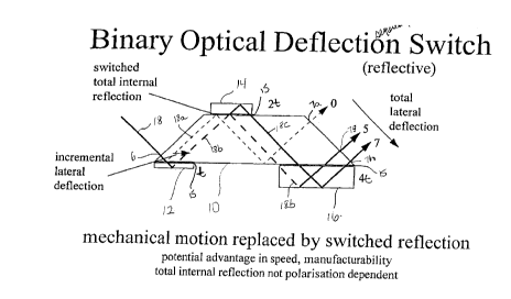
Referring now to Fig. la, a binary optical deflection switch is shown comprised of a
trapezoidal shaped block 10 having an input port 6 and having output ports 7a to 7h,
wherein ports 7a, 7g, and 7h are shown. The block 10 is made of light transmissive
material such as glass. Light tr:~nsmissive glass blocks 12, 14 and 16 having three
25 different thicknesses t, 2t, and 4t and having the same re*active index as the trapezoidal
shaped block 10 are shown to be adjacent the block 10, and spaced from the block 10 by
a thin layer of silicone 15 having a re*active index that is substantially the same as the
glass blocks or an equivalent resilient index matching buffer material.
30 A more basic lx2 optical switch is shown in Fig. lb having a single input port and two
output ports. An input beam is launched from the left of the figure into a block of glass 6.
- -
CA 02221200 1997-11-14
DocNo. 10-90 Patent
When the glass block 7 (and its buffer material not shown) is optically contacting the
block 6, light is routed to port 1. When the glass block 7 is moved so that it does not
contact the block 6, light is routed to port 0. The thickness t of the block 7 will determine
the spacing between ports 0 and 1.
s
Referring now to Fig. 2, two glass blocks, for example 12 and 16 shown in Fig. 1 are
illustrated in greater detail. Spring like members 20 are merely illustrative of means for
positioning the blocks 12 and 16 along and off of an edge of the block 10 respectively. Of
course any suitable positioning means that that has a fast enough response time such as
o solenoids or piezoelectric actuators can be used.
The operation of the reflective elements shown in Fig. 2 will now be described. An
incident beam of light 22 is shown propagating from the left of the figure directed to the
right in the direction of the arrow. The beam first passes through the interface at the
surface 10, the silicon material 15 and propagates through the block 12 to reflect off its
upward face 12a demonstrating total internal reflection due to the refractive index
difference between that of the block and the air adjacent to it. The beam then passes
through the elastomer (silicon) 15 and into the block 10 as the elastomer and block 10
have substantially the same refractive index as the glass block 12. The beam then reflects
20 off the lower surface of the block 10 and is directed toward the block 16. However, block
16 is not making contact with the glass block 10 so it is reflected back downward due to
the glass 10 / air interface that is present. Thus when the elastomer attached to either of
the blocks 12 or 16 are in contact with the surface of 10, the location of the reflection
point is moved outward, and the path length of a given segment 22a, 22b, or 22c is
25 lengthened by the travel through the block 12 or 16.
The operation of the switch can now readily be understood with reference to Fig. 1.
Although not shown, the blocks 12, 14, and 16 are individually controllably movable
such that they are in contact with the block 10 (via the elastomer index matching
30 material) or such that they are lifted off of the block 10. By way of example, several, but
not all of the possible selectable paths are shown through the lines 1 8a, 1 8b, and 1 8c
- -
CA 02221200 1997-11-14
Doc No. 10-90 Patent
which lead to ports 0, 5, and 7 respectively. As a beam of light 18 is launched into the
input port 6 of the switch at a predetermined angle, it is either reflected off the air/10
interface or the air/12 interface, depending upon whether block 12 is not, or is, in
contact (via the elastomer) with block 10. In the first instance when there is contact
s between the blocks 10 and 12, the beam 18 reflects off the outward face of the block 12
and follows the path shown by dotted line 1 8b. In the second instance when there is no
contact between the blocks 10 and 12, the beam 18 reflects off the face 10 and follows
the path defined by line 1 8a. Depending upon whether blocks 14 and 16 are lifted off or
are in contact with the block 10 will determine which path is followed. The positioning
o of the blocks 12, 14, 16 adjacent sequential reflective surfaces of the block 10 is
determined by the initial launch angle. It should be noted that for a switch with n blocks
(i.e. here n=3 for blocks 12, 14, and 16), that there are 2n output ports. For example in this
instance, where n = 3, the following switching combinations are possible.
12 14 16
off off off
off off on
off on off
off on on
20 on off off
on off on
on on off
on on on
2s Referring now to Figs. 3a and 3b, a comparison is made, wherein it is shown that three
two-state devices are required in accordance with this invention to provide switching
between a single input port and eight output ports. In contrast an optical switch having a
conventional binary tree configuration requires seven two-state devices to achieve the
same functionality.
CA 02221200 1997-11-14
DocNo. 10-90 Patent
In Fig. 4 an alternative embodiment of the invention is shown wherein a block 40 having
6 sides and 5 individually movable blocks 42a.. 42e having thicknesses t, 2t, 4t, 8t, and
1 6t provide a lx32 optical switch. Using even multiples of t ensures that the output ports
will be substantially evenly spaced.
s
The optical switches described heretofore in accordance with this invention, can be used
as a lxn switch, or alternatively, can be ganged with several other same switches to
provide an nxn optical switch. This is illustrated in Figs. 5a and Sb.
o Of course numerous other embodiments of the invention may be envisaged, without
departing from the spirit and scope of the invention.