Note: Descriptions are shown in the official language in which they were submitted.
CA 02221214 1997-11-17
-1-
CIRCUIT AND METHOD FOR TRACKING FINGER OFF-SET IN
A SPREAD-SPECTRUM RAKE RECEIVER AND
WIRELESS INFRASTRUCTURE EMPLOYING THE SAME
TECHNICAL FIELD OF THE INVENTION
The present invention is directed, in general, to
wireless communications and, more specifically, to a circuit
and method for tracking finger off-set in a spread-spectrum
rake receiver and a wireless infrastructure, such as Code
Division Multiple Access ("CDMA"), employing the same.
BACKGROUND OF THE INVENTION
The ever increasing availability and popularity of
wireless communication can be linked to technological gains
that have provided more efficient, reliable and cost-
effective mobile devices, such as wireless digital
telephones and personal communication systems ("PCSs"), as
examples. Due to their mobility and low power requirements,
conventional mobile devices impose significant design
constraints upon the wireless communication networks and,
more particularly, the switching offices that support them.
Each switching office is associated with multiple
transceiver sites, or "cells," that enable communication
between the mobile devices and the switching office.
Typically, there is a high density, or closeness, of cells
per geographic area, often in a honeycomb pattern of
overlapping cells of communication. Cell density causes each
mobile device to always be "close" to at least one cell.
Thus, any wireless signal may be concurrently heard by
several cells and, possibly; several switching offices.
Each cell generally covers a range of several miles in each
direction, which may of course be limited by natural or man
made objects -- mountains, buildings, etc.
In the past, wireless communication was largely analog-
based, but in recent years, the wireless carriers have moved
CA 02221214 1997-11-17
-2-
toward digital-based communications. This transition stems
from compatibility and frequency utilization perspectives --
if users can share a frequency or a range of frequencies,
then more users can be accommodated on less bandwidth.
An increasingly popular wireless digital communication
methodology is Code Division Multiple Access ("CDMA"). CDMA
is a version of "older" spread spectrum technologies.
Spread spectrum technology, introduced in the 1920s, has
evolved over a number of decades from uses in secured
military applications to conventional civilian wireless
communication applications_
More particularly, spread spectrum technology provides
a means for organizing radio frequency energy over a
somewhat wide range of frequencies and moving among the
frequency range on a time divided basis. As an example, a
transmitter transmits at a first frequency at a first time
and at a second frequency at a second time; a receiver
receiving these transmissions is synchronized to switch
frequencies during reception in response to the change from
the first to the second frequency.
Whenever multiple signals are communicated through a
communication network, the potential for losing data or
degradation of the communication signal may increase
exponentially. Maintaining a synchronized signal among a
transmitter and a receiver is therefore paramount. If the
synchronization, or timing, of transmission or arrival of a
signal is off, then the information content of the signal
may be distorted or lost -- this phenomenon is commonly
referred to as "slippage."
Searching for and tracking of a communication signal
are therefore two of the most important synchronization
processes performed by the receiver. The searching process
operates to find or locate possible signal paths in order to
demodulate the strongest received communication signal (as
well as to provide candidates for soft handoff).
CA 02221214 1997-11-17
-3-
The tracking process, in contrast, operates to track a
received communication signal. This is often accomplished
using a "tracking loop." Conventional tracking loops work
to fine-tune the signal path, most often to a static
pseudorandom number ("PN") chip. Since a received signal
may be transmitted at any one of a number of data rates, the
lowest possible data rate is most often assumed -- only a
small portion of all the data received is used for the
tracking process, resulting in an inefficient tracking loop.
Therefore, what is needed in the art is an adaptive
means for tracking a received signal wherein a convergence
rate of the tracking means is made to depend upon the data
rate of the received signal. Tr~hat is further needed in the
art is a tracking means that follows changes in signal delay
due to movement and reference timing adjustments of a mobile
device.
SUN~ARY OF THE INVENTION
To address the above-discussed deficiencies of the
prior art, the present invention provides a finger tracking
circuit for a rake receiver, a method of tracking a carrier
signal and a wireless infrastructure. The finger tracking
circuit includes: (1) a timing error subcircuit that
determines a timing error in a current power control group
("PCG") of a carrier signal to be tracked and (2) a feedback
subcircuit that applies a gain signal that is a function of
a data rate of the carrier signal and a signal-to-noise
("SNR") of the carrier signal to the timing error
subcircuit; a convergence rate of the finger tracking
circuit therefore depending on the data rate of the carrier
signal which may be suitably derived from a strength of the
carrier signal.
The present invention therefore introduces the concept
of adapting the gain signal applied to the timing error
subcircuit as a function of the data rate and the SNR of the
CA 02221214 1997-11-17
-4-
carrier signal. The convergence rate of the finger tracking
circuit therefore is made to depend indirectly upon carrier
signal strength (which usually correlates with the carrier
signal's SNR): the higher the data rate of the carrier
signal, the faster the convergence, and vice versa. In a
most preferred embodiment, the finger tracking circuit takes
the form of a phase-locked loop ("PLL") to aid continued
carrier signal tracking.
In one embodiment of the present invention, the gain
signal is a function of an energy content of the PCG.
Energy content of the PCG depends, in part, on carrier
signal amplitude, from which the data rate and the signal to
noise ratio may be derived (defined). Those skilled in the
art will understand that other characteristics of the
carrier signal or its associated PCGs may be used to adapt
the gain signal. The broad scope of the present invention
is not limited to using any particular characteristic of the
carrier signal to perform gain signal adaptation.
In one embodiment of the present invention, the gain
signal approximates unity when the carrier signal is at a
predetermined nominal energy level. In a most preferred
embodiment, the gain signal is zero when either no carrier
signal is present or the SNR is approaching zero -- which is
equivalent to switch "off." Of course, the gain signal does
not need to be normalized. Certain applications may make
advantageous use of non-normalized gain signals.
In one embodiment of the present invention, the
feedback subcircuit comprises a loop filter coupled between
prefilter and postfilter multipliers, the feedback circuit
applying a gain factor derived from the amplitude to the
prefilter and postfilter multipliers. Of course, the broad
scope of the present invention requires neither a loop
filter or multipliers. In fact, in an alternative
embodiment of the present invention, the feedback subcircuit
comprises a loop filter coupled between prefilter and
~.
CA 02221214 1997-11-17
-5-
postfilter bit shifters, the feedback circuit applying a
gain factor logarithmically derived from the amplitude to
the prefilter and postfilter shifters. Those skilled in the
art will recognize that the present invention may be
embodied in analog or digital discrete or integrated
circuitry.
Alternatively, the timing error and feedback
subcircuits may embodied as a sequence of instructions
executable in data processing circuitry. The present
invention may take the form of software executable in
general purpose data processing and storage circuitry or
signal processing circuitry, as appropriate. The broad
scope of the present invention is not limited to a
particular hardware, firmware or software embodiment.
In one embodiment of the present invention, the timing
error subcircuit applies a Walsh demodulation (a Walsh index
derived from the demodulation process) to the carrier signal
to determine the timing error in the PCG. Those skilled in
the art are familiar with Walsh demodulation. The present
invention can make advantageous use of Walsh demodulation to
develop the timing error that is provided to the feedback
subcircuit.
The foregoing has outlined, rather broadly, preferred
and alternative features of the present invention so that
those skilled in the art may better understand the detailed
description of the invention that follows. Additional
features of the invention will be described hereinafter that
form the subject of the claims of the invention. Those
skilled in the art should appreciate that they can readily
use the disclosed conception and specific embodiment as a
basis for designing or modifying other structures for
carrying out the same purposes of the present invention.
While the present invention is embodied in hardware,
alternate equivalent embodiments may employ, whether in
whole or in part, firmware and software. Those skilled in
CA 02221214 1997-11-17
-6-
the art should also realize that such equivalent
constructions do not depart from the spirit and scope of the
invention in its broadest form.
BRIEF DESCRIPTION OF THE DRAWINGS
For a more complete understanding of the present
invention, reference is now made to the following
descriptions taken in conjunction with the accompanying
drawings, in which like numbers designate like objects, and
in which:
FIGURE 1 illustrates a block diagram of an exemplary
PRIOR ART circuit that embodies a conventional finger
tracking algorithm;
FIGURE 2 illustrates a block diagram of an exemplary
circuit that embodies an exemplary finger tracking algorithm
of the present invention;
FIGURE 3 illustrates a flow diagram of an exemplary
finger tracking algorithm according to the principles of the
present invention;
FIGURE 4 illustrates a block diagram of an exemplary
integrated circuit that embodies the exemplary finger-
tracking algorithm of FIGURES 2 and 3 according to the
principles of the present invention; and
FIGURE 5 illustrates a high-level block diagram of an
exemplary infrastructure within which the embodiments
illustrated in FIGURES 2 to 4 of the present invention may
be suitably associated.
DETAILED DESCRIPTION
Before undertaking a detailed description of a PF2IOR ART
finger tracking circuit (FIGURE 1) and several advantageous
embodiments illustrating the principles of the present
invention (FIGURES 2 to 5), it may be helpful to set forth
an environment within which the present invention may be
associated. "Spread spectrum," as the phrase is used
CA 02221214 1997-11-17
_'j_
herein, is an umbrella term that refers generally to any
modulation technique in which the data or information
content of a wireless communication signal is spread over a
wider bandwidth than the frequency content of the original
S data or information signal upon which it is based -- the
modulation technique operates to take an input signal and
spread it over a typically broad frequency range. "Code
Division Multiple Access" ("CDMA," also direct sequence
("DS")-CDMA), as the phrase is used herein, is a known
wireless communication methodology based upon spread
spectrum technology -- major benefits of CDMA are increased
capacity and efficient use of the transmission spectrum.
It should be noted that the term "include" and
derivatives thereof, as used herein, mean inclusion without
limitation; that the phrase "associated with" and
derivatives thereof, as used herein, may mean to include
within, interconnect with, contain, be contained within,
connect to or with, couple to or with, be communicable with,
juxtapose, cooperate with, interleave, be a property of, be
bound to or with, have, have a property of, or the like; and
that the term "or," as used herein, is inclusive, meaning
and/or.
Turning initially to FIGURE 1, illustrated is a PRIOR
ART circuit (generally designated 100) that embodies a
conventional finger tracking algorithm. PRIOR ART circuit
100 may be suitably associated with a conventional rake
receiver and illustratively includes each of a sampler
circuit 105, an early gate circuit 110, a late gate circuit
115, an adder circuit 120, a loop filter circuit 125 and a
two switching circuits 130 and 135.
Sampler circuit 105 receives a carrier signal (e.g., a
complex digital communication signal) and a control signal
(i.e., an output signal received from loop filter 125) as
inputs and generates each of an early signal (T-o) and a
late signal (T+o). Early gate circuit 110 and late gate
CA 02221214 1997-11-17
_g_
circuit 115 respectively receive the early signal and the
late signal and a control signal (e. g., a conventional Walsh
Index, which may be suitably derived from a conventional
demodulation process) as inputs and operate to gate the
early and late signals as inputs to adder circuit 120.
Adder circuit 120 combines the early and late signals to
generate a timing error output signal having an amplitude
that is proportional to the difference of the early and late
signals' amplitudes. The timing error signal is input to
loop filter circuit 125 to generate the control signal for
sampler circuit 105.
Noise significantly affects performance of the above-
illustrated tracking loop of PRIOR ART finger tracking
circuit 100. Using CDMA as an example, noise is especially
acute for conventional CDMA reverse link receiver systems
(e. g., IS-95 standard), which use conventional data burst
randomization ("DBR") for different data rates. If a timing
error, ~, signal is gated "off" in a current power control
group ("PCG"), the timing error signal may consist of
nothing but noise, which may have a large magnitude.
According to PRIOR ART teachings, narrow bandwidth and
small loop gains are chosen for tracking loops under "noisy"
conditions to mitigate this problem. This approach
effectively disables the tracking loop and results in very
slow convergence. An alternate PRIOR ART approach enables
the tracking loop for gated "on" PCG only. Since a carrier
signal may be transmitted at any one of a plurality of data
rates ( e, g. , ~/s, 1/, 1/z, 1, etc . pseudorandom number ( "PN" )
chip), a lowest data rate (e.g., ~/s PN chip) is assumed --
only two out of sixteen possible PCGs may be used for the
finger tracking operation, resulting in an inefficient
tracking loop.
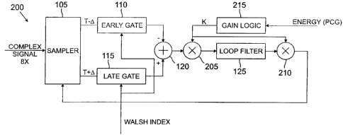
Turning now to FIGURE 2, illustrated is a block diagram
of an exemplary circuit (generally designated 200) that
embodies an exemplary finger tracking algorithm of the
CA 02221214 1997-11-17
-9-
present invention. Exemplary finger tracking circuit 200
may suitably be associated with a conventional rake receiver
of a conventional wireless infrastructure (discussed with
reference to FIGURE 5) and illustratively includes each of
a sampler circuit 105, an early gate circuit 110, a late
gate circuit 115, an adder circuit 120, a loop filter
circuit 125, two multiplier switching circuits 205 and 210,
and a gain logic circuit 215.
Sampler circuit 105 receives a carrier signal and a
control signal (i.e., an output signal received from loop
filter 125) as inputs and generates each of an early signal
(T-o) and a late signal (T+o). Early gate circuit 110 and
late gate circuit 115 respectively receive the early signal
and the late signal and a control signal (e.g., a
conventional Walsh Index) as inputs and operate to gate the
early and late signals as inputs to adder circuit 120.
Adder circuit 120 combines the early and late signals to
generate a timing error output signal having an amplitude
that is again proportional to the difference of the early
and late signals' amplitudes. The timing error signal is
input to loop filter circuit 125 via first multiplier
switching circuit 205. Loop filter circuit 125 generates
the control signal and communicates the same to sampler
circuit 105 via second multiplier switching circuit 210.
Exemplary sampler circuit 105, early gate circuit 110,
late gate circuit 115, adder circuit 120 and first and
second multiplier switching circuits 205 and 210
cooperatively comprise a timing error subcircuit that
determines a timing error in a current PCG of the carrier
signal being tracked.
According to the illustrated embodiment, first and
second multiplier switching circuits 205 and 210 are
controlled by gain logic circuitry 215. Gain logic
circuitry 215 and first and second multiplier switching
circuits 205 and 210 cooperatively comprise a feedback
CA 02221214 2000-07-10
-10-
subcircuit that applies a gain signal, K, that is a function of
a data rate of the carrier signal and a signal-to-noise
("SNR") of the carrier signal to the timing error
subcircuit, and more particularly to sampler circuitry 105.
A convergence rate of finger tracking circuit 200 depends on
the data rate of the carrier signal which may be suitably
derived from a strength of the carrier signal.
Since the carrier signal may be transmitted at any one
of a plurality of data rates ( e. g. , ~/$, 1/, i/x, 1, etc. PN
chip), the present embodiment, particularly the feedback
subcircuit, operates to adapt the gain signal applied to the
timing error subcircuit as a function of the data rate and
the SNR of the carrier signal. The convergence rate of
finger tracking circuit 200 is therefore made to depend upon
carrier signal strength (which usually correlates with the
carrier signal's SNR) -- stronger (the higher the data rate
of) the carrier signal, the faster the convergence, and vice
versa. Finger tracking circuit 200 is adaptive and unlike
PRIOR ART circuit 100 of FIGURE 1 does not operate statically
at the lowest data rate (e. g., '/s PN chip) -- all possible
PCGs may be used .for the finger tracking operatior~ of finger
tracking circuit 200, resulting in an efficient tracking
loop.
Alternatively, the timing error and feedback
subcircuits may be embodied as a sequence of instructions
executable in data processing circuitry. The present
invention may take the form of software executable in
general purpose data processing and storage circuitry or
signal processing circuitry, as appropriate. The broad
scope of the present invention may be suitably implemented
in hardware, firmware, software, or suitable combinations of
the same: In point of fact, any suitable processing
configuration may be used, including programmable
processors, programmable logic devices, such as programmable
array logic ("PALs") and programmable logic arrays ("PLAs"),
CA 02221214 1997-11-17
-11-
digital signal processors ("DSPs"), field programmable gate
arrays ("FPGAs"), application specific integrated circuits
("ASICs"), large scale integrated circuits ("LSIs"), very
large scale integrated circuits ("VLSIs") or the like, to
S form the various types of circuitry, controllers and systems
described and claimed herein.
It should also be noted that finger tracking circuit
200 has illustratively taken the form of a phase-locked loop
("PLL") aiding continued carrier signal tracking.
Turning now to FIGURE 3, illustrated is a flow diagram
of an exemplary finger tracking algorithm (generally
designated 300) according to the principles of the present
invention. For purposes of illustration, finger tracking
algorithm 300 is discussed with reference to finger tracking
circuit 200 of FIGURE 2, which may be associated with a
conventional rake receiver of a wireless spread spectrum
infrastructure.
To begin, a carrier signal to be tracked is received by
the rake receiver of a wireless spread spectrum
infrastructure (input/output step 305). Finger tracking
circuit 200 determines a timing error in a current PCG of
the received carrier signal (process step 310). According
to the illustrated embodiment, the timing error subcircuit
applies a Walsh demodulation to the carrier signal to
determine the timing error in the PCG. Those skilled in the
art are familiar with Walsh demodulation. The present
embodiment may make advantageous use of Walsh demodulation
to develop the timing error that is provided to the feedback
subcircuit.
Finger tracking circuit 200 determines a gain signal as
a function of the energy content of the PCG of the received
carrier signal (process step 315). Energy content of the
PCG depends, in part, on carrier signal amplitude, which may
be suitably used to determine (derive) a data rate of the
carrier signal. Those skilled in the art will understand
CA 02221214 2000-07-10
-12-
that other characteristics of the carrier signal may be used
to adapt the gain signal. It should be noted that the broad
scope of the present embodiment is not limited to using any
particular characteristic of the carrier signal to perform
gain signal adaptation.
It should also be noted that while the present
embodiment illustrates the substantially concurrent
performance of process steps 310 and 315, these steps may be
performed sequentially and in any suitable order.
In one embodiment of the present invention, the gain
signal approximates unity when the carrier signal is at a
predetermined nominal energy level. In a most preferred
embodiment, the gain signal is zero when either no carrier
signal is present or the SNR is approaching zero -- which is
equivalent to switch "off." Of course, the gain signal does
not need to be normalized and certain applications may make
advantageous use of non-normalized gain signals.
Finger tracking circuit 200, and particularly the
feedback subcircuit, comprises a gain logic circuit 215
(e. g., a loop filter) coupled between a first multiplier
switching circuit 205 (e.g., a prefilter multiplier) and a
second multiplier switching circuit 210 (e. g., a postfilter
multiplier). The feedback circuit applies a gain factor
derived from the amplitude to multiplier switching circuits
205 and 210 (process, step 320), a convergence rate of finger
tracking circuit 200 therefore depending on the data rate
and the SNR of the carrier signal, which may be suitably
derived from the strength of the carrier signal.
The broad scope of the present invention requires
neither a loop filter or multipliers. In point of fact, in
an alternate embodiment, the feedback subcircuit comprises
a loop filter coupled between prefilter and postfilter bit
shifters, the feedback circuit applying a gain factor
logarithmically derived from the amplitude to the prefilter
and postfilter shifters. Those skilled in the art will
CA 02221214 2000-07-10
-13-
recognize that the present invention may be embodied in
analog or digital discrete or integrated circuitry.
To summarize, exemplary finger tracking algorithm 300
adapts the gain signal applied to the timing error
subcircuit as a function of the data rate and the SNR of the
carrier signal. The convergence rate of finger tracking
circuit 200 is therefore made to depend upon carrier signal
strength (which usually correlates with the carrier signal's
SNR) -- the higher the data rate of the carrier signal, the
faster the convergence, and vice versa.
Turning now to FIGURE 4, illustrated is a block diagram
of another exemplary circuit (again generally designated
200) that may suitably embody exemplary finger tracking
algorithm 300 of FIGURE the present invention. Exemplary
finger tracking circuit 200 illustratively includes each of
a timing error subcircuit (e.g., a sampler circuit 105, a
suitably arranged multiplexes 405, conventional Walsh
demodulation circuit 410, a multiplier 415 and a suitable
delay circuit 420) and a feedback subcircuit (e.g., a
prefilter shifter circuit 210, a loop filter circuit 125, a
postfilter shifter circuit 205 and gain logic circuit 215).
Finger tracking circuit 200 may be suitably associated
with a conventional a rake receiver for tracking a carrier
signal. The exemplary timing error subcircuit is operative
Z5 to determine a timing error in a current PCG of a received
carrier signal to be tracked. The exemplary feedback
subcircuit is operative to apply a gain signal that is a
function of the data rate and the SNR of the carrier signal
to the timing error subcircuit, a convergence rate of finger
tracking circuit 200 depending on the data rate derived from
strength of the received carrier signal.
Turning now to FIGURE 5, illustrated is a high-level
block diagram of an exemplary infrastructure (generally
designated 500) within which the embodiments of FIGURES 2 to
4 of the present invention may be suitably associated.
CA 02221214 1997-11-17
-14-
Exemplary infrastructure 500 employs CDMA and includes a
single Switching and Distribution Unit ("SDU") 505, a
plurality of cells 510a and 510b employing rake receivers
and a single mobile station 515.
Exemplary SDU 505 may suitably refer to any
conventional base station, typically fixed, that is
associated with a plurality of wireless cell sites (e. g.,
cells 510a and 510b) and is used by mobile units for
communication with other mobile units or conventional land
line communication networks (e.g., public, private) and
telephony stations associated with the same.
Although the present embodiment illustrates single SDU
505 and only two cell sites, those skilled in the art
understand that an infrastructure according to the
principles of the present invention may include a plurality
of base stations and more than two cell sites. These bases
stations and cell sites typically cooperate, or communicate,
via wire-based interconnections therebetween.
Exemplary SDU 505 illustratively includes a switch 520,
a speech coder 525 and an interface 530. Exemplary switch
520 may be any conventional suitably arranged device
operative to open or close circuits, complete or break
electric paths, select circuits, select/control
communication paths or the like. "Device," as the term is
used herein, means any apparatus, contrivance, machine,
mechanism or the like that may be implemented electrically,
mechanically, electro-mechanically, electronically,
optically or the like to perform at least one function or
arrive at some result. Exemplary speech/voice coder 525 may
be any conventional suitably arranged device operative to
convert a speech/voice input received in one format to an
output transmitted in another format. Exemplary interface
530 may be any conventional suitably arranged device
operative to associate wireless infrastructure 500 with
another base station or conventional communications network,
CA 02221214 1997-11-17
-15-
which according to the present illustration is a public
switched telephone network ("PSTN") (not shown) as an
example.
Exemplary SDU 505 is illustratively associated with a
S Mobile Switching Center ("MSC") 535. Exemplary MSC 535 may
be any conventional suitably arranged device operative to
coordinate and control a plurality of cell sites, and, in
particular, is responsible for processing CDMA soft-handoff
requests.
Each of exemplary cells 510a and 510b is illustrative
of a basic geographic unit of a wireless communication
system (e. g., infrastructure 500), deriving its name largely
from a geographic "honeycomb-type pattern" of cell site
installations (typically, each city, county, region or the
like is divide into smaller "cells"). Each of cells 510a
and 510b may be any conventional suitably arranged device
operable as a receiver and transmitter (e. g., a rake
transceiver) of wireless carrier, or communication, signals
(carrier signals not only include voice/speech signals, but
may also include data signals and any associated control
information). Thus, according to the illustrated
embodiment, the rake transceivers, which may be suitably
associated with the base stations, communicate wirelessly
with at least mobile station 515 via carrier signals carried
on a plurality of spread-spectrum fingers.
Each exemplary cell 510a, 510b illustratively includes
amplifiers 540, radios 545, a cell site control 550 and a
network interface 555. Each exemplary amplifier 540 may be
any conventional suitably arranged device operative to
strengthen a signal, such as a carrier signal of the present
illustration -- when telephone conversations travel through
a medium, such as a copper wire, an optical fiber, a
wireless channel or the like, they encounter resistance and
thus become weaker and more difficult to receive. Each
exemplary radio 545 may be any conventional suitably
CA 02221214 1997-11-17
-16-
arranged device operative to communicate communication
signals distantly by converting the same to and from
electromagnetic waves broadcast wirelessly through airspace
(e.g., spread spectrum). Exemplary cell site control 550
may be any conventional suitably arranged device operative
to control/manage a plurality of channels within a cell, as
well as to respond to control messages from MSC 535, to
report statuses to MSC 535, etc. Exemplary network
interface 555, similar to exemplary PSTN interface 530, may
be any conventional suitably arranged device operative to
associate its cell 510 with SDU 505.
According to the illustrated embodiment, a finger
tracking circuit 200 of the present invention is associated
with at least one of the rake transceivers. Finger tracking
circuit 200 tracks at least one of carrier signal, and
includes each of a timing error subcircuit and a feedback
subcircuit as described with reference to FIGURES 2 to 4.
The timing error subcircuit operates to determine a timing
error in a current PCG of the at least one carrier signal,
and the feedback subcircuit operates to apply a gain signal
that is a function of a data rate and the SNR of the carrier
signal to the timing error subcircuit. A convergence rate
of finger tracking circuit 200 therefore depends on the data
rate of the carrier signal, which may be derived from the
strength of the carrier signal tracked.
Exemplary mobile station 515 is associated with each of
cells 510a and 510b, and may be any conventional suitably
arranged device operative to receive and transmit wireless
carrier signals with cell sites. In addition to wireless
telephony, such as cellular telephones, personal
communication systems ("PCS") or the like, mobile station
515 may also be a wireless processing system, such as a
portable computer, data terminal or the like.
Conventional data communications is more fully
discussed in each of Data Communications Principles, by R.
CA 02221214 2000-07-10
-17-
D. Gitlin, J. F. Hayes and S. B. Weinstein, Plenum Press
(1992), in The Irwin Handbook of Telecommunications, by
James Harry Green, Irwin Professional Publishing (2nd ed.
1992) and in Voice & Data Communications Handbook, by Bud
Bates and Donald Gregory, McGraw-Hill (1996); and
conventional electronic circuit and computer or processing
system and network design are more fully discussed in
Art of Electronics, by Paul Horowitz and Winfield Hill,
Cambridge (2nd ed. 1989); in Data Network Design, by Darren
L. Spohn, McGraw-Hill, Inc. (1993); and in Computer
Organszatson axed Architecture, by William Stallings,
MacMillan Publishing Co. (3rd ed. 1993).
From the above, it is apparent that the present
invention provides a finger tracking circuit for a rake
receiver, a method of tracking a carrier signal and a
wireless infrastructure. The finger tracking circuit
includes: (1) a timing error subcircuit that determines a
timing error in a current PCG of a carrier signal to be
tracked and (2) a feedback subcircuit that applies a gain
signal that is a function of a data rate and the SNR of the
carrier signal to the timing error subcircuit, a convergence
rate of the finger tracking circuit therefore depending on
the data rate of carrier signal, which may be derived from
the strength of the carrier signal.
Although the present invention has been described in
detail, those skilled in the art should understand that they
can make various changes, substitutions and alterations
herein without departing from the spirit and scope of the
invention in its broadest form.