Note: Descriptions are shown in the official language in which they were submitted.
CA 02221443 1997-11-18
WO 96/38855 PCT/US96/08237
DESCRIPTION
Fabrication Process for Hermetically Sealed Chamber in Substrate
TECHNICAL FIELD
This invention relates in general to integrated microelectronic devices and
relates more particularly to devices having a simplified construction
especially adapted
for use in displays and to simplified methods of fabricating such
microelectronic
devices, including methods for fabricating a hermetically sealed chamber in a
substrate.
BACKGROUND OF THE INVENTION
Field-emission displays are considered an attractive alternative and
replacement
1o for liquid-crystal displays, because of their lower manufacturing cost and
lower
complexity, lower pov~er consumption, higher brightness, and improved range of
viewing angles. Microelectronic field-emission devices more generally are also
attractive alternatives to semiconductor devices for many applications, being
capable of
high performance and being capable of fabrication from a wide range of
materials with
15 less stringent controls of material purity, but with fabrication processes
and equipment
similar to those used for semiconductor fabrication. A review article on the
general
subject of vacuum microelectronics was published in 1992: Heinz H. Busta
"Vacuum
Microelectronics - 1992," in Journal of Micromechanics and Microengineering,
Vol. 2,
No.-2 (June 1992). An article by Katherine Derbyshire, "Beyond AMLCDs: Field
20 Emission Displays?" in Solid State Technology, Vol. 37 No. 11 (Nov. 1994)
pages 55-
65, summarized fabrication methods and principles of operation of some of the
competing designs for field-emission devices and discussed some applications
of field-
emission devices to flat-panel displays. The theory of cold field emission of
electrons
from metals is discussed in many textbooks and monographs, including the
monograph
25 by R. O. Jerkins and W. G. Trodden, "Electron and Ion Emission From Solids"
(Dover
Publications, Inc., New York, NY, 1965), Chapter 4
NOTATIONS AND NOMENCLATURE
The terms emitter and cathode are used interchangeably throughout this
specification to mean a field-emission cathode. The term "control electrode"
is used
3o herein to denote an electrode that is analogous in function to the control
grid in a
vacuum-tube triode. Such electrodes have also been called "gates" in the field-
emission device related art literature. Ohmic contact is used herein to denote
an
electrical contact that is non-rectifying. Phosphor is used in this
specification to mean
a material characterized by cathodoluminescence. In descriptions of phosphors,
a
35 conventional notation is used wherein the chemical formula for a host or
matrix
CA 02221443 1997-11-18
WO 96/38855 PCT/US96/08237
2
compound is given first, followed by a colon and the formula for an activator
(an
impurity that activates the host crystal to luminesce), as in ZnS: Mn, where
zinc sulfide
is the host and manganese is the activator.
DESCRIPTION OF THE RELATED ART
Microelectronic devices using field emission of electrons from cold-cathode
emitters have been developed for various purposes to exploit their many
advantages
including high-speed switching, insensitivity to temperature variations and
radiation,
low power consumption, etc. Most of the microelectronic field-emission devices
in the
related art have had emitters which point orthogonally to the substrate,
generally away
from the substrate, but sometimes toward the substrate. Examples of this type
of
device are shown, for example, in U.S. Pat. No. 3,789,471 by Spindt et al.,
U.S. Pat.
No. 4,721,885 by Brodie, U.S. Pat. No. 5,127,990 by Pribat et al., U.S. Pat.
Nos.
5,141,459 and 5,203,731 by Zimmerman, and in the above-mentioned article by
Derbyshire. In such structures, the anode is typically a transparent faceplate
parallel to
the substrate and carrying a phosphor which produces the display's light
output by
cathodoluminescence. A few cold-cathode microelectronic devices have had field
emitters oriented in a plane substantially parallel to their substrates, as
for example in
U.S. Pat. No. 4,728,851 by Lambe, U.S. Pat. No. 4,827,177 by Lee et al., and
U.S.
Pat. Nos. 5,233,263 and 5,308,439 by Cronin et al. The terminology "lateral
field
2o emission" and "lateral cathode" or "lateral emitter" of the latter two
patents by Cronin
et al. will be adopted herein to refer to a structure in which the field
emitter tip or
blade edge points in a lateral direction, i.e. substantially parallel to the
substrate. In
such lateral cathode structures of the prior art the anode is oriented
substantially
orthogonally to the substrate and to the emitter (as in U.S. Pat. Nos.
5,233,263 and
5,308,439 by Cronin et al.), or is coplanar with the emitter (as in U.S. Pat.
No.
4,827,177 by Lee et al.), or requires a transparent substrate (as in U.S. Pat.
No.
4,728,851 by Lambe). Some device structures and fabrication processes using
lateral
cathode configurations have been found to have distinct advantages, such as
extremely
fine cathode edges or tips and precise control of the inter-element
dimensions,
3o alignments, capacitances, and of the required bias voltages.
CA 02221443 1997-11-18
WO 96/38855 PCT/US96/08237
3
PROBLEMS SOLVED BY THE INVENTION
If lateral field-emission devices are used in a display cell with phosphor-
coated
anodes, a number of problems occur. In some of the prior art structures, the
cathodoluminescence occurs only at a very narrow region at an edge of the
anode
facing the lateral emitter. In others the light emitted from the phosphor can
be
obscured by opaque electrodes or absorbed in the phosphor layer itself or in a
faceplate. In some prior art structures very high anode voltages must be used.
For
low voltage electron field-emission device display elements (e.g. with anode
potentials
of less than about 10 volts with respect to the emitter), the actual electron
penetration
1o into the phosphor is on the order of 1 nanometer. Therefore, in displays
using prior art
lateral electron field-emission device display elements, the light emission
due to
cathodoluminescence occurs along the edge of the phosphor facing the emitter
element. Furthermore, other electron field-emission displays such as the
Spindt type
(described in the patent by Spindt et al. and in the review article by H. H.
Busta cited
15 herein above) typically emit light at a phosphor surface which is opposite
the phosphor
surface facing the observer.
The device structure described herein has a lateral electron emitter situated
a
distance above the anode phosphor. With an appropriate applied bias, the
emitted
electrons spread out over the top surface of the phosphor and impinge over a
wider
2o area of the phosphor element than with other lateral electron field-
emission device
display elements. Hence, with this new structure, the light is emitted in
direct view of
the observer and is not attenuated by passing through the phosphor as is the
case with
prior art structures. Also, the light is generated over a larger portion of
the cell area
than in prior art structures. The prior art descriptions of lateral-emitter
field-emission
25 display elements do not show how to provide a bias voltage contact to the
phosphor of
such an anode element. The new structure described herein has a metal anode
contact
situated below the phosphor ("buried") and also may have means for connecting
to that
buried contact from the surface for applying electrical bias. In particular,
the simplified
structure may be fabricated within a hermetically sealed chamber in the
substrate.
3o While the lateral-emitter type of construction has the distinct advantages
described above, those lateral-emitter field-emission devices heretofore
available
having the most precise control of inter-element dimensions and alignment have
been
somewhat expensive to fabricate because of the relatively large number of
materials
and process steps used. Those process steps have included steps using
conformal
35 layers of sacrificial materials needed to form spacers that define some of
the
dimensions. The present invention eliminates some of the materials and process
steps
needed for fabrication, thus reducing fabrication time and cost and also
providing a
CA 02221443 1997-11-18
WO 96/38855 PCT/US96/08237
4
simplified anode structure, while retaining the advantages of lateral cathode
construction and inherently automatic alignment of the lateral cathode type of
design.
This simpler structure and simpler, less expensive fabrication are effective
both for
field-effect devices having phosphor anodes used for display elements and for
field-
ei~ect devices without phosphor. Thus the present invention solves several
problems
existing in the prior art.
PURPOSES, OBJECTS, AND ADVANTAGES OF THE INVENTION
An important object of the invention is providing a display with improved
light
emission from each cell of the display. A related object is a field-emission
device
to structure specially adapted for use in a display cell. Another related
object is a field-
emission display which allows light emitted from a phosphor to be aimed more
directly
toward the viewer of the display. Another related object is a field-emission
display cell
structure in which the light emission area occupies a larger portion of the
cell area than
in prior art devices of the lateral-emitter type. Another object of the
invention is a
15 metallization structure that allows the other features and advantages of an
improved
lateral-emitter field-emission display device to be realized. A particular
object is an
anode electrical contact structure that does not obscure any portion of a
phosphor
surface of a display cell. A related object is an anode contact that can act
as a mirror
to reflect emitted light toward the observer of the display. Another object is
a display
20 cell anode structure that provides improved performance with coulombic
aging of the
phosphor thereby being reduced or eliminated. Another particular object is a
display
cell simplified by having a control electrode configuration that may be made
with a
single metallization step. An overall object of the invention is an improved
display
which nevertheless retains all the known advantages of lateral-emitter field-
emission
25 devices, including the following: extremely fine cathode edges or tips;
exact control of
the cathode-to-anode distance (to reduce device operating voltage and to
reduce
device-to-device variability); exact control of the cathode-to-control-
electrode distance
(to control the control-electrode-to-cathode overlap, and thereby control the
inter-
electrode capacitances and more precisely control the required bias voltage);
inherent
3o alignment of the control-electrode and cathode structures; self alignment
of the anode
structure to the control-electrode and cathode; and improved layout density.
Another
object of the invention related to retaining known advantages of lateral-
emitter field-
emission devices is the significant design flexibility provided by an
integrated structure
which reduces the number of interconnections between devices, thus reducing
costs
35 and increasing device reliability and performance. Another important object
of the
invention is a process using existing microelectronic fabrication techniques
and
apparatus for making integrated lateral-emitter field-emission display device
cell
CA 02221443 2001-06-12
WO 96/38855 PCTIUS96/08237
structures with economical yield and with precise control and reproducibility
of device
dimensions and alignments. A major object of the invention is a simplified
anode structure
for lateral-emitter field-emission devices. Another major object of the
invention is a
fabrication-process which eliminates some masks otherwise needed for
fabrication of a
self aligned lateral-emitter field-emission device, thus reducing fabrication
time and cost.
SUMMARY OF THE INVENTION
Under a first broad aspect of the invention, a field-emission device is made
with a
lateral emitter substantially parallel to a substrate and with a simplified
anode structure.
The lateral-emitter field-emission device has a thin-film emitter cathode
which has a
thickness of not more than several hundred angstroms and has an emitting blade
edge or tip
having a small radius of curvature. The simplified anode device may also have
one or more
control electrodes. The anode's top surface is precisely spaced apart from the
plane of the
lateral emitter and receives electrons emitted by field emission from the
blade edge or tip of
the lateral-emitter cathode, when a suitable bias voltage is applied. The
device may be
configured as a diode, or as a triode, tetrode, etc. having one or more
control electrodes
positioned to allow control of current from the emitter to the anode by an
electrical signal
applied to the control electrode. In a particularly simple embodiment, a
single control
electrode is positioned in a plane above or below the emitter edge or tip and
automatically
aligned to that edge. The simplified devices are specially adapted for use in
arrays,
including field-emission display arrays.
Under a second broad aspect of the invention, a novel fabrication process
using
process steps similar to those of semiconductor integrated circuit fabrication
is used to
produce the novel devices and their arrays. Various embodiments of the
fabrication process
allow the use of conductive or insulating substrates and allow fabrication of
devices having
various functions and complexity. The anode is simply fabricated, without the
use of prior
art processes which formed a spacer made by a conformal coating. In a
preferred
fabrication process for the simplified anode device, the following steps are
performed: an
anode film is deposited; an insulator film is deposited over the anode film;
an ultra-thin
conductive emitter film is deposited over the insulator and patterned; a
trench opening is
reactive ion etched through the emitter and insulator, stopping at the anode
film, thus
forming and automatically aligning an emitting edge of the emitter; and means
are provided
for applying an electrical bias to the emitter and anode, sufficient to cause
field emission of
electrons from the emitting edge of the emitter to the anode. The anode film
may comprise
a phosphor for a device specially adapted for use in a field-emission display.
The
fabrication process may also include steps to deposit additional insulator
films and to
CA 02221443 2001-06-12
WO 96/38855 PCTIUS96/08237
6
deposit additional conductive films for control electrodes, which are
automatically aligned
with the emitter blade edge or tip.
Under a third broad aspect, the invention provides a process for forming an
evacuated chamber in a substrate having an upper surface. The process
comprises the steps
of:
- providing a first opening having a first predetermined depth and a
predetermined
volume in the upper surface of the substrate such as to form a main cavity;
- providing a second opening having a second predetermined depth and which
communicates with the first opening;
- temporarily filling both the first and the second openings with a
sacrificial first
material;
- planarizing the sacrificial first material to form a planar surface;
- disposing a second material over the upper surface of the substrate and the
planar
surface to form a chamber ceiling;
- providing a third opening in the chamber ceiling only over the second
opening;
- removing the sacrificial first material from beneath the chamber ceiling
through the
third opening to form a chamber;
- removing any atmosphere surrounding and within the chamber formed to
evacuate
the chamber;
- introducing a gettering material into the third opening; and
- then immediately introducing a third material into the second and third
openings,
while plugging the third opening and while sealing the third material to the
second
material, thereby enclosing the evacuated chamber.
Under a fourth broad aspect, the invention provides a process for forming a
gas-
filled chamber in a substrate having an upper surface. The process comprises
the steps o~
- providing a first opening having a first predetermined depth and a
predetermined
volume in the upper surface of the substrate such as to form a main cavity;
- providing a second opening having a second predetermined depth, and which
communicates with the first opening;
- temporarily filling both the first and the second openings with a
sacrificial first
material;
- planarizing the sacrificial first material to form a planar surface;
- disposing a second material over the upper surface of the substrate and the
planar
surface to form a chamber ceiling;
- providing a third opening in the chamber ceiling only over the second
opening;
CA 02221443 2001-06-12
WO 96/38855 PCTIUS96/08237
6a
- removing the sacrificial first material from beneath the chamber ceiling
through the
third opening to form a chamber;
- removing any atmosphere surrounding and within the chamber formed to
evacuate
the chamber;
S - introducing gas at a desired pressure into the chamber,
- introducing a gettering material into the third opening; and
- immediately introducing a third material into the second and third openings
while
plugging the third opening and while sealing the third material to the second
material, thereby enclosing the gas-filled chamber.
BRIEF DESCRIPTION OF THE DRAWINGS
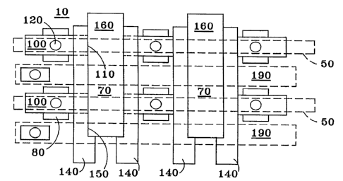
Fig. 1 shows a plan view of a portion of a preferred array embodiment of field-
emission devices made in accordance with the invention.
Fig. 2 shows a side elevation cross-sectional view of an embodiment of a
single
field-emission device made in accordance with the invention.
Fig. 3 shows a side elevation cross-sectional view of an alternate embodiment
of a
single field-emission device.
Figs. 4a and 4b together show a flow diagram of an embodiment of a fabrication
process performed in accordance with the invention.
Figs. Sa and Sb together show a series of side elevation cross sectional views
corresponding to results of the process steps of Figs. 4a and 4b.
DETAILED DESCRIPTION OF THE PREFERRED EMBODIMENTS
Fig. 1 shows a plan view of a portion of a preferred array embodiment of field-
emission devices made in accordance with the invention. In the simple array of
Fig. 1, each
field-emission device shares an anode with at least one other device, and each
anode is
shared by two or more devices. Some of the emitters in Fig. 1 are also shared
by two
devices. This sharing of elements between devices is not necessary for use or
operation of
the invention, but it is sometimes useful in designing and fabricating arrays
with higher
density (in terms of the number of devices per unit area). The basic features
of devices
CA 02221443 2001-06-12
WO 96/38855 PCTIUS96/08237
6b
made in accordance with the invention may be clearly understood by considering
the single
device of Fig. 2.
Fig. 2 shows a side elevation cross-sectional view of an embodiment of a
single
field-emission device made in accordance with the invention. The field-
emission device,
denoted generally by 10, is made on a flat substrate 20. A layer of insulator
30 has a top
major surface, which defines a reference plane 40 convenient for description
of other
elements. A layer of conductive material 50 may be used as a buried contact
layer. It
should be noted that conductive layer 50 may lie on the reference plane, as
shown in Fig. 2,
or may be made by depositing conductive layer 50 into recesses formed in
insulator 30 and
by planarizing the resulting surface. In the latter case the top surface of
conductive layer 50
lies in reference plane 40. A layer of insulator 60 is
CA 02221443 1997-11-18
WO 96/38855 PCT/US96108237
made on the reference plane 40, covering conductive layer 50. A conductive
layer
parallel to plane 40 serves as an anode 70. As will become apparent from a
reading of
the remainder of this specification and the appended claims, the preferred
fabrication
process described herein below automatically places the top surface of anode
70 below
the plane of lateral emitter 100. For embodiments such as that of Fig. 2, in
which
some devices have independent anodes, the anodes of adjacent devices are
separated
and insulated from each other by regions of an insulator 80. At the left side
of Fig. 2, a
small portion of the anode 70 of an adjacent device is shown to the left of
insulator 80;
that portion is not involved in the structure or operation of the single
device of the
to present description. An insulating layer 90 of predetermined thickness is
made parallel
to the substrate. An ultra-thin conductive layer which forms an emitter layer
100 is
also made parallel to the substrate and patterned, thus forming a lateral
emitter. A
conductive contact 120 may connect emitter layer 100 to buried contact layer
50. If
the device is to have a control electrode 140 above emitter 100, then two
additional
15 layers are made: a layer of insulator 130 and a conductive layer patterned
to form a
control electrode 140. In the fabrication process for this device (described
more fully
herein below), an opening 160 is provided by employing a directional etch.
That
opening extends through all the layers of conductors and/or insulators lying
above the
anode down to the top surface of anode 70. The process of etching opening 160
forms
2o an blade edge or tip 110 where lateral-emitter thin film 100 terminates
after the etch.
The blade edge or tip 110 has a very small radius of curvature, limited by
half the
thickness of the ultra-thin lateral-emitter layer 100. Preferred thicknesses
of lateral-
emitter film 100 are less than about 300 angstroms, which limit the radius of
curvature
of lateral-emitter blade edge or tip to be less than about 150 angstroms.
Those skilled
25 in the art will recognize that the radius of curvature is a significant
factor in producing
an electric field at tip 110 sufficient to cause cold-cathode field emission
at a low
applied bias voltage, and that the radius of curvature may be somewhat less
than half
of the film thickness. Another factor significant in determining the electric
field
ei~ective in causing field emission is the (predetermined) thickness of
insulator film 90.
3o The degree of film thickness control in conventional semiconductor
integrated
processing is sufficient to control the thickness of insulator film 90 to the
desired
precision. Devices made in accordance with the present invention may be
operated at
applied bias voltages of 10 to 50 volts or even less. In the preferred
embodiment of
Fig. 2, anode 70 extends at least partially under lateral emitter 100. That
is, anode 70
35 extends beyond the vertical plane through emitting edge 110 defined by the
side wall of
opening 160.
It should be noted that conductive connections to the various electrodes of
the
device may be made in a conventional manner, and are therefore not shown in
the
CA 02221443 1997-11-18
WO 96138855 PCT/US96/08237
8
drawings. These conductive connections may be made, for example, by vertical
studs
that lie outside the plane of the side elevation cross-section view of Fig. 2.
For
example, a conductive stud may extend from emitter 100 and/or buried contact
layer
50 to a surface conductive pad to which the emitter bias voltage may be
applied. A
similar conductive connection, electrically isolated from the emitter
connection, may be
made to anode 70, for application of the anode bias voltage. Similarly,
conductive
connections are needed to apply control signals to control electrodes) 140 if
the
device is a triode or tetrode, etc. having such control electrodes. The
arrangement just
described may also be reversed, in the sense that the emitter connection may
be made
to directly to a surface pad, and buried contact layer 50 may be used for
anode contacts.
Of course, for field emission of electrons to occur, the polarity of applied
bias voltages
must be such that the anode is positive with respect to the emitter. Various
devices
made on the same substrate need not have identical physical arrangements of
conductive connections. Some devices may have buried anode contacts, while
other
15 devices on the same substrate may have buried emitter contacts. Such
arrangements
allow for compact and efficient circuit layout in circuits in which an emitter
of one
device is to be connected to an anode of another device. With such
arrangements,
dissimilar connections lying in the same plane and not intended to be
connected may be
kept electrically independent by being spaced laterally and/or by having
intervening
2o insulator material disposed between them, as is known in the art.
Fig. 3 shows a side elevation cross-sectional view of an alternate embodiment
of a single field-emission device made in accordance with the invention. The
lateral-
emitter field-emission device of Fig. 3 is a diode device, without a control
electrode.
The anode of the device shown in Fig. 3, denoted generally by 70, includes a
phosphor
25 layer 75, which is a part of anode 70. If the anode phosphor is conductive,
the entire
anode 70 may consist of phosphor. The anode 70 of Fig. 3 is shown with a
separately
identified phosphor film 75 to illustrate an alternative embodiment. The
device of Fig.
3 also differs from Fig. 2 in that anode 70 does not extend beneath emitting
blade edge
or tip 110 of lateral emitter 100. Another way of describing the alternative
structure
3o shown in Fig. 3 is that opening 160, the sidewall of which defines the
vertical plane
containing emitting edge 110 of lateral emitter 100, extends beyond the
horizontal
extent of anode 70. However the vertical extent of opening 160 is still
determined by
the fact that opening 160 extends vertically only to the top surface of anode
70 (which
in this embodiment is the top surface of phosphor film 75). The minimum
vertical
35 extent of opening 160 in the device of Fig. 3 is the sum of the
predetermined thickness
of insulator layer 90 and the predetermined thickness of lateral emitter 100.
The field-
emission device may be made with a plurality of anodes 70 (not shown in the
drawings). A usefi.~l example of such a structure has three anodes per
emitter, with a
CA 02221443 1997-11-18
,..
_9_ /f~fj . ~~~96
different phosphor color of each anode. A particularly useful combination is a
three-
anode device with red, green, and blue phosphors for an RGB display.
Operable and preferred materials for the various structural elements of the
lateral-emitter field-effect device with simplified anode are described herein
below in
connection with an exposition of a novel and preferred fabrication process.
A novel fabrication process using process steps similar to those used in
semiconductor integrated circuit fabrication may be used to produce the
devices and
their arrays in accordance with the invention. Various embodiments of the
fabrication
process allow the use of conductive or insulating substrates and allow
fabrication of
1o devices having various functions and complexity. A notable feature of all
the
fabrication process embodiments described herein is that the anode is simply
formed
without the use of a spacer employed in some prior art processes. (In those
prior art
processes, a spacer was formed by a sacrificial conformal coating.)
Figs. 4a and 4b together show a flow diagram of an embodiment of a
fabrication process performed in accordance with the invention. Fig. Sa - Fig.
Sr show
a series of side elevation cross sectional views corresponding to results of
the process
steps of Figs. 4a and 4b. In the following description of a preferred process
for
fabricating field-emission devices, reference is made to Figs. 4a, 4b, and Sa -
Sr, in
which the same or similar process steps and the device side elevation cross-
sectional
2o views of results corresponding to those steps are both denoted by the same
step
references S1, S2, ..., 518. A simple overall process outline for fabrication
of a diode
device is described first, followed by a description of the detailed process
which is
depicted in Figs. 4a and 4b and which is further illustrated by the
corresponding results
of Figs. Sa - Sr. Table I lists the process steps shown in Figs. 4a and 4b.
In a simple fabrication process for a diode field-emission device with
simplified
anode, the following steps are performed: an anode film 70 is deposited (S7);
an
insulator film 90 is deposited (S8) over the anode film; an ultra-thin
conductive emitter
film 100 is deposited (S12) over the insulator and patterned; a trench opening
160 is
etched (S15) through the emitter and insulator, stopping at the anode film,
thus
3o forming and automatically aligning an emitting edge 110 of the emitter; and
means are
provided (S18) for applying an electrical bias to the emitter and anode,
sufficient to
cause field emission of electrons from the emitting edge 110 of the emitter
100 to the
anode 70. The anode film 70 deposited in step S7 may comprise a phosphor film
75
for a device specially adapted for use in a field-emission display. The
phosphor may be
any cathodoluminescent material, and may be selected on the basis of its
conductivity
and/or the color of its luminescence.
:;
CA 02221443 1997-11-18
WO 96/38855 PCT/US96/08237
S1 Provide substrate
S2 Deposit insulating layer
5 S3 Pattern and etch recesses
S4 Deposit conductive material in recesses to form buried contact
layer
SS Planarize
S6 Deposit insulating layer
S7 Deposit conductive layer to a predetermined thickness
to S8 Deposit insulating layer to a predetermined thickness
S9 Deposit conductive layer to form control electrode layer
S10 Deposit insulating layer to a predetermined thickness
S11 Provide conductive contacts to buried contact layer
S12 Deposit and pattern ultra-thin emitter layer
S13 Deposit insulating layer to a predetermined thickness
S14 Deposit and pattern control electrode layer if any
S15 Provide opening down to anode top surface
S16 Open contact holes to emitter, control electrode (if any)
and anode
contact
2o S17 Deposit metal contacts
S18 Provide means for applying suitable bias and signal voltages)
Table I. List of fabrication process steps shown in Figs. 4a and 4b.
CA 02221443 1997-11-18
s;~ j'# ;~ : s : i - r1 v,: ._ - l
< < , _, .,
l~.i_~.:
A fabrication process for a triode, tetrode, etc. device may also include
steps to
deposit additional insulator films 130 and to deposit additional conductive
films 140
for control electrodes, which have a control electrode edge 150 automatically
aligned
with the emitter blade edge or tip 110. In the following detailed process
description,
these additional steps are included as "optional" steps, to be performed only
if control
electrodes are to be included in a particular device structure. It will be
apparent to one
skilled in the art that the detailed process of Figs. 4a and 4b, illustrated
by the results
of Figs. Sa - Sr, may be modified to fabricate simpler devices by omitting
particular
process steps as appropriate. Other variations in technique and in the order
of process
l0 steps will also be apparent to one skilled in the art.
A detailed description of a preferred process for fabricating the field-
emission
devices now proceeds, with reference to Figs. 4a, 4b, and Sa - Sr.
To fabricate a triode device with one or two control electrodes, the process
illustrated in Figs. 4a, 4b, and Sa - Sr is performed. A substrate 20 is
provided (step
S1), which may be a silicon wafer. An insulating layer 30 is deposited (step
S2) on the
substrate. This may be done, for example, by growing a film of silicon oxide
approximately one micrometer thick on a silicon substrate. A pattern is
defined on the
insulator surface for depositing a conductive material. In the preferred
process, a
pattern of recesses is defined and etched (step S3) into the surface of the
insulator
layer. In step S4, metal is deposited in the recesses to form a buried contact
layer 50,
which is then planarized (step SS). While this is described here as a metal
deposition,
the conductive material deposited in step S4 may be a metal such as aluminum,
tungsten, titanium, etc., or may be a transparent conductor such as tin oxide,
indium tin
oxide etc. (For applications using a common emitter for all devices made on a
substrate, the substrate may be conductive and perform the function of a
buried emitter
contact. For such applications, steps S2, S3, S4, and SS may be omitted,
although a
step similar to step S2 may be required to insulate a control electrode if any
from the
substrate.) An insulating layer 60 is deposited (step S6). This may be a
chemical
vapor deposition of silicon oxide to a thickness of about 0.1 to 2
micrometers, for
3o example.
A conductive layer is deposited (step SZ) to a predetermined thickness and
patterned to form an anode layer 70. If anode 70 is not required to be
cathodoluminescent in order to fixnction as a light source, then the
conductive anode
layer 70 deposited in step S7 may be a metal film or another conductive film
such as
indium oxide or indium tin oxide (ITO). If the device is to be used in a light-
emitting
application, such as a display, the conductive layer may be a conductive
phosphor 75
or may be a composite layer comprising a conductive material with a thin film
of
CA 02221443 1997-11-18
~,~~~~~ ~, ~ >;a~.~ '~~96
-12-
phosphor 75 on its top surface. Suitable phosphors include zinc oxide(Zn0),
zinc
sulfide (ZnS) and many other compounds. Some other suitable phosphors are
ZnO:Zn; Sn02:Eu; ZnCia204:Mn; La202S:Tb; Y202S:Eu; LaOBr:Tb;
ZnS:Zn+In203; ZnS:Cu,Al+In203; (ZnCd)S:Ag+In203; and ZnS:Mn+In203.
Still other suitable phosphor materials are described, for example, in the
chapter by
Takashi Hase et al. "Phosphor Materials for Cathode Ray Tubes" in "Advances in
Electronics and Electron Physics" Vol. 79 (Academic Press, San Diego, CA,
1990),
pages 271-373, which reference also uses the conventional phosphor notation
used
here. If the application requires anode layer 70 to be patterned, that
patterning may be
to done by subprocesses that are conventional in semiconductor fabrication
practice,
using lithography and etching to pattern the layer. In particular, anode layer
70 may be
formed and patterned by a process analogous to steps S3, S4, and S5.
In the next step (S8), an insulating layer 90 is deposited to a precisely
predetermined thickness. This predetermined thickness of insulating layer 90
is quite
important in determining the emitter-to-anode closest distance, and thus in
determining
the electric field produced by a given applied bias voltage. Step S8 may
comprise
chemical vapor deposition of silicon oxide to a predetermined thickness in the
range of
0.1 to 2 micrometers, for example.
Steps S9 and S10 are performed if a control electrode layer 140 is needed
2o below the emitter layer 100. (Such a control electrode layer is shown in
Figs. Si - 5j,
but then omitted from Figs. 5k- 5r to illustrate the option without a lower
control
electrode layer.) If needed, a conductive control electrode layer 140 is
deposited and
patterned in step S9. In step S10 an insulating layer 130 of a predetermined
thickness
is deposited over conductive control electrode layer 140 to insulate it and to
provide a
flat insulating surface parallel to the substrate for the next step. Whether
or not steps
S9 and S10 are performed, a planar insulating surface is provided.
This description of a fabrication process continues with reference to Fig. 4b
and Figs. Sk - 5r, respectively showing the remaining fabrication steps and
the
corresponding side cross sectional views of the device. In step 511,
conductive
3o contacts 120 are provided to the buried contact layer 50, by opening
suitable contact
holes and depositing conductive material in them (forming "studs") to make
ohmic
contact with buried contact layer 50. In step Si2, an ultra-thin emitter layer
100 is
deposited and patterned. Preferred materials for conductive lateral-emitter
layer 100
are titanium, tungsten, tantalum, molybdenum, or their alloys such as titanium-
tungsten
alloy. However, many other conductors may be used, such as aluminum, gold,
silver,
copper, copper-doped aluminum, platinum, palladium, polycrystalline silicon,
etc. or
transparent thin-film conductors such as tin oxide or indium tin oxide (ITO).
It is very
CA 02221443 1997-11-18
WO 96/38855 PCT/US96/08237
13
desirable to use a material with a low work function for electron emission. In
this
respect, preferred materials have work functions less than three electron
volts, and
even more preferred materials have work fiznctions of less than one electron
volt. The
deposition in step S17 is controlled to form a film preferably of about 100 -
300
angstroms thickness in order to have an emitter blade edge or tip 110 in the
final
structure that has a radius of curvature preferably less than 150 angstroms
and more
preferably less than 50 angstroms. To fabricate the preferred embodiment of
Fig. 2,
patterning of lateral emitter 100 is done so that lateral emitter 100 extends
over at least
a portion of anode 7U~. An insulator 130 is deposited (step S13) over the
emitter layer.
to Again this may be a chemical vapor deposition of silicon oxide to a
thickness of about
0.1 to 2 micrometers, for example. If there are to be two control electrodes
and if
symmetry with respect to the plane of emitter layer 100 is desired, then this
insulator
layer 130 should be made the same thickness as the insulator layer 130
deposited in
step 510. If a control electrode 140 is to be incorporated, a conductive
material is
15 deposited and patterned (step S14) to form the upper control electrode
layer 140.
(The control electrode 140 may be deposited in a recess pattern and
planarized, as in
the case of the buried. contact layer 50.) It should be mentioned that the
conductive
films deposited and patterned in steps S4, S9 (if performed), S12, and S14 (if
performed) are all deposited in at least partial alignment with respect to the
anode film
20 70 deposited and patterned in step S7.
In step S15, an opening is provided through all the layers lying over anode
70,
down to the top surface of anode layer 70. This opening is patterned to
intersect at
least some portions of emitter layer 50 (and of control electrode layers 140
if any), to
define emitting edge 110 of emitter layer 100 (and to define edge 150 of
control
25 electrode layer 140 if any). This step is performed by using conventional
directional
etching processes such as reactive ion etching sometimes called "trench
etching" in the
semiconductor fabrication literature. To fabricate the preferred embodiment of
Fig. 2,
step S15 is performed while leaving at least a portion of insulator 90
remaining and
covering at least a portion of anode 70.
3o In step 516, contact holes are opened to emitter, control electrode, and
anode
if needed. Metal contacts are deposited where needed in step 517.
Alternatively, this
part of the process (steps S16 and S17) may be performed after step S13 or S14
but
before S15. It that case, the sequence of process steps would be as follows:
513, S14
(if used), S16, 517, and then S15. It should be noted that for some display
35 applications (such as so-called "heads-up" displays), it is desirable to
form the device
structure using substantially transparent materials for all the films. With
the operable
and preferred thicknesses of the films in the present invention, such
transparent films
may be made if desired.
CA 02221443 1997-11-18
A ~~f~ . S
-14-
In step 518, means are provided for applying suitable electrical bias
voltages,
and (for devices incorporating control electrodes) suitable signal voltages.
Such means
may include, for example, contact pads selectively provided at the device top
surface
to make electrical 'contact, and optionally may include wire bonds, means for
tape
automated bonding, flip-chip or C4 bonding, etc. In use of the device, of
course,
conventional power supplies and signal sources must be provided to supply the
appropriate bias voltages and control signals. These will include providing
sufficient
voltage amplitude of the correct polarity (anode positive) to cause cold-
cathode field
emission of electron current from emitter edge 110 to anode 70. If desired, a
1o passivation layer may be applied to the device top surface, except where
there are
conductive contact studs and/or contact pads needed to make electrical
contacts. This
completes the description of the detailed process illustrated in Figs. 4a, 4b,
and Sa - 5r.
If it is desired to have the field-emission cell operating with a vacuum or a
low
pressure inert gas in opeung 160, it is necessary to enclose that space or
cavity (FIGS.
6 and 7). This can be done by a process similar to that described in the
anonymous
publication "Ionizable Gas Device Compatible with Integrated Circuit Device
Size and
Processing," publication 30510 in "Research Disclosure", Number 305, September
1989. Such a process can be begun by etching a small auxiliary opening 210,
connected to the opening provided in step 515, but preferably not as deep as
that
opening (i.e. preferably not extending as deeply as the level of anode layer
70). This
auxiliary opening 210 may be made at a portion of the cavity spaced away from
the
emitter edge area 110. The opening 160 for the main cavity and the connected
auxiliary opening 210 are both filled temporarily with a sacrificial organic
material,
such as parylene, and then planarized. An inorganic insulator 220 is
deposited,
extending over the entire device surface including over the sacrificial
material, to
enclose the cavity. A hale 230 is made in the inorganic insulator by reactive
ion
etching only over the auxiliary opening 210. The sacrificial organic material
is
removed from within the cavity by an etch, such as an oxygen plasma etch,
which
operates through the hole 230. The atmosphere surrounding the device is then
3o removed to evacuate the cavity. If an inert gas filler is desired, then
that gas is
introduced at the desired pressure. Then the hole and auxiliary opening are
immediately filled by depositing, e.g. sputter-depositing, an inorganic
material 240 to
plug the hole. If introduction of a gettering material 250 is desired, the
hole-plugging
step may consist of two or more substeps: viz. depositing a quantity of getter
material
250, and then depositing_an inorganic material 240 such as an insulator to
complete the
plug. The plug of inorganic material seals the cavity and retains either the
vacuum or
any inert gas introduced. The gettering material 250, if used, is chosen to
getter any
undesired gases, such as oxygen or gases containing sulfur, for example. Some
CA 02221443 1997-11-18
~~ J
suitable getter materials are Ca, Ba, ~Ti, alloys of Th, etc. or other
conventional getter
materials known in the art of vacuum tube construction.
It will be appreciated by those skilled in the art that integrated arrays of
field-
emission devices, such as the array of Fig. 1, may be made by simultaneously
performing each step of the fabrication process described herein for a
multiplicity of
field-emission devices on the same substrate, while providing various
interconnections
among them. An integrated array of field-emission devices made in accordance
with
the present invention has each device made as described herein, and the
devices are
arranged as cells containing at least one emitter and at least one anode per
cell. The
to cells are arranged along rows and columns, with the anodes interconnected
along the
columns for example, and the emitters interconnected along the rows.
INDUSTRIAL APPLICABILITY
There are many diverse uses for the hermetically sealed chamber, device
structures, and fabrication processes of this invention, especially in making
flat panel
15 displays for displaying images and for displaying character or graphic
information with
high resolution. It is expected that the type of flat panel display made with
the device
of this invention can replace many existing displays including liquid crystal
displays,
because of their lower manufacturing complexity and cost, lower power
consumption,
higher brightness, and improved range of viewing angles. Displays made in
accordance
2o with the present invention are also expected to be used in new applications
such as
displays for virtual reality systems. In embodiments using substantially
transparent
substrates and films, displays incorporating the structures of the present
invention are
especially useful for augmented-reality displays.
Other embodiments of the invention will be apparent to those skilled in the
art
25 from a consideration of this specification or from practice of the
invention disclosed
herein. For example the order of process steps may be varied to some extent
for
various purposes; improved lithographic patterning, deposition, etching, or
other
process techniques may be used; functionally equivalent materials may be
substituted
for the particular materials used in the embodiments, described herein;
preferred
30 dimensions may be varied; and other modifications may be made to adapt the
device to
various usages and conditions. The hermetically sealed chamber may be used to
enclose and protect various microelectronic devices other than field-emission
devices.
It is intended that the specification and examples be considered as exemplary
only, with
the true scope and spirit bf the invention being defined by the following
claims.
35 Having described my invention, I claim: