Note: Descriptions are shown in the official language in which they were submitted.
CA 02221693 1997-11-20
WO 96/4I40S PCT/GB96/01376
- 1 -
Optical ~mrl;f;~r
Fidld of tlhc Invention
This ;nvention relates to an optical amplifier, particularly a semiconductor
5 opticaLl ~mplifi.-r having non-linear characteristics.
Background
It is known that s~ ico..~ rtors can act as optical amplifiers. When certain
S~miconrll-rtQrs are subject to an injectecl electric current, an inri~ent photon
Jo causes an electron to ~r~c.~C semiconductor's gap band with the result that an
additional photon is generatet thereby producing light amplifir~tion.
Semiconductor optical amplifiers which operate in this way are well known
and reference is directed to" Long Wavelength Semiconductor Lasers" G. P.
Agrawal and N. K. Dutta; Van Nostrand, Chapters 1 to 6.
The s~mirorttlllctQr material which is used as the active amplific~tion region of
the device may comprise a bulk materi~l or for example, a stack of multiple
qV~rltllm wells (MQW). A problem with the semiconduaor material that is
usecl for the amplification region is that it suffers from a gain-saturation effect
20 whicb may be produced by amplified spontaneous emission (ASE). For this
reason, typical devices that use bulk semiconductor material in a parallel sided~h~nn~l, usually have a length of 500 microns or less and a width of 1-2
microns, because if the device were to be made longer, there would be no
i~lplo~..lle.l~ in gain. For MQW devices, the gain per unit length is slightly
lower than for bulk material devices, and ~mplifitors of length up to 1 mm
have been produced hitherto but it has been considered that devices of longer
lengtl~ would suffer from ASE, with no il~rov~ e~lL in gain. Lo~ger, tapered
devices have been reported, of length 1-3mm, in which tapering of the
amplifier is ar~ gc~ to offset partially the onset of gain saturation. Referencer 30 iS directed to S. El Yumin et al, " Taper Shape DepPn~ nre of Tapered-Waveguide Travelling Wave S~mirQr,~~~rtQr Amplifier", IEICE T~ ;ons
on ]_le~ ~.u~i~, Vol. e77, No 4, April 1994, Tokyo Japan. Reference is also
CA 02221693 1997-11-20
W O 96/41405 PCT/GB96/01376
- 2 -
directed to D. Mehuy~ et al, " 11.6 W Peak power LrL~Lion limited diode-to-
diode optical amplifier" Appl. Phy. Lett. Vol. 62, No 6, 8th ~d~iudly 1993,
pp544-546, which ~ic~loses a broad area travelling wave amplifier of width 600
,Lm and length ~'~O01~m
Another disadvantage of longer devices is that they are harder to mount.
ConvPntionqlly~ SOAs are mounted using headers ~ 1 for laser diodes,
which tend to be shorter and as a result, it is not straightforward to pa kag~P
longer devices.
Also, longer devices consume more power, so that it has been considered
disadvantageous for the device to be longer than that at which optical
saturation occurs.
15 Semiconductor optical amplifier devices can be used for a number of d;rr~lc,
purposes and a review is given in K. E. Stubkjaer et al,nOptical Wavelcng~h
Convertersn, Proc. ECOC '94, pp 63~642. SOAs can be used as modulators,
in which an optical signal, mo-llllatPd at a given bit rate, is fed into the
amplifier, together with a separate target wave. The mnr~ te~l signal
20 produces gain-saturation for s..c~c~,;ve bits and as a result, the target wave is
morilll~te~l with the input bit pattern. This is known as cross gain
morllllation (XGM). The modulation may also produoe a phase shift in the
target wave and this is known as cross phase modulation (XPM). Both of
these ~r~.c~ses may produoe w~.lcngth conversion. For ~ample, the target
25 wave souroe may be at a d;rL~ wdvc:le-,~,~h to the mo~ te~ input souroe
so that the bit mod~ tiQn is transferred from the input optical source at a
first wd~ele~Lh to the target wave at a second d;rL.c.l~ w~
In order for the mo~lllqtor to be crL~lvc~ for exarnple in an optical data
30 ~ sion nc~wvlL, it is desirable that the amplifier exhibit ul~lr~llll
amplifi.~qtion ch~ ..;stics over a wide range of bit mor~lllqtion freq .Pnt~ c
For example, Stubkjaer s~pra al.g~ ~ a bit rate ~ .lcy to more than 5-
CA 02221693 1997-11-20
W O 96/41405 PCT/GB96/01376 -3-
10 G-bit/s. A bit rate of 20 ~bitJs has been .~o-~ed by J. M. Wi~ 3~.~r~k~, J.
S. Perino, A. H. Gnauk and B. Glance, "Bit Error Rate P~.rul~ce for
Wi~rr lcnE,~L Conversion at 20 ~Bitls", Electron. Lett. 30, pp 720-721 (1994)
~lthollgh it is not clear from Wir~. ..r. kl et al whether the mn~ tor was
5 O~ dLlng within a 3 db bandwidth.
Hitherto, it had been considered that che bandwidth was limited by the
d~r~ ;al carrier .~eo...bination rate in the arnplifier, this rate inrlu~ling
spontaneous emission ant stim~ r~l emission.
However, in accordance with the present invention, it has been found that the
-3 db bandwidth of the gain of the amplifier in respect of the bit moc~.l~tiQr
rate, is a function of the length of the path through the amplifier. Thus, in
accordance with the invention, it Ihas been appreciated that by in. l~ashlg the
length of the path, this bandwidth can be increased.
Selmiconductor amplifiers can also be used to produce wdv~le~gth co~v~,~;on
by a d;rr~,e.l~ process known as four wave mi~ing This is rlicrl.cce~l in
Stubkjaer s~pra and a fuller theoretical ~lic~lccion is given in n Population
20 pulsations and non-lPgen~rate four-wave mixing in semiconductor lasers and
amplifiers" G. P. Agrawal, J. Opt. Soc. Am. B, Vol 5, No 1, Januar~ 1988
ppl47-159. In four wave mi~ring~ pump radiation at a pump w~v~lcngth ~p is
fed into a semiconductor amplifiler, ~ogether with an input signal ~; of a
d;rr~.~... wavclc.~ h to the pump signal. In a typical example, the pump
w~vr~rurlll has an energy of lOmLw whereas the input signal has an energy of
lmw~. The w~lcnE,~L of the input signal is close to that of the pump,
typically with a w~ len~Lh d;L~ ce of ~ 2nm. The two beams are of the
s~ne polarisation and consc~luently beat cohe.c..-ly, with a beat L~lu_~cy in
this example of ~ 100 GHz. The reslllt~nt beat w<~efollll causes the carrier
30 tensity in the amplifier to os~ te. This produces a non-linear effect on the
gai~n~ which lags the input w.~ f~ and beats with it. It can be shown that
this produces a ~. d~ len~,~L col~ ed signal ~c~ with a w~L~elc.~ L
CA 02221693 1997-11-20
W O 96/41405 PCT/GB96/01376
-4-
~c--2~p - ~;. The co~ c.Led signal ~c and the input signal ~; are equally
spaced in terms of wd~k~l~;LL above and below the pump w~el~n~;L ~p.
Four wave mixing has the a.l~ ~e that the col,~ ;on process is csLl~lld~
5 fast as it does not rely on carrier ~ecohlbilld~ion as in XGM and XPM.
Furthermore, there is less distortion but four wave mixing suffers from the
disddv ul~age that the coll~.Led signal is of low power and the signal to noise
ratio can be a problem in respect of the converted signal.
o However, in accordance with the invention, it has been found that the
ccl,v~,~;on PffiriPn~y for four wave ~miYing is function of the length of the
path through the amplifier. Thus, in accordance with the invention, it has
been ~ypr~c;dLed that by in~ledsing the length of the path, the four wave
mixing effiri.-ncy can be increased.
~5
Sull~llla.y of the Invention
In accordance with the invention from a first aspect, there is provided a
semiconductor optical amplifier ayyar~ s inrl~l-ling an optical path from an
input to an output through an optical amplification region of sl.bst~nti~lly
20 cor~ct:~nt widrh of less than 50~m along its length, the path having a length through the region that exceeds 1 mm.
In another aspect, the invention provides optical ay~ar~us comprising a target
wave source, a modulated optical source that is mrJ~ te~ at a given bit rate,
25 and an optical amplifier to receive radiation from the sources and oy~d~ive
to produce mo~llll~tirn of the target wave according to the mr~ tion of the
mr~ t~o~l optical source wLc.~,by to produce a mn~lnl t~" target wave
output, wl,e.~;n the amplifier has an optical path from an input to an output
through an optical amplifir~tion region and the length of the path is s~lr~
30 to be longer than that at which optical saturation in said region occurs.
Also, in aocol~ll~ce with the invention there is provided optical mor~ tiQn
CA 02221693 1997-11-20
W 0916/~1405 PcTl~L~ 376
-5-
d~ lUd~ ,0 ~;sing a target wave source, a mr~ Pr~ optical source that is
mnf~ tPA at a given bit rate, an optical mr!ifiPr to receive rs~iqtirJn from
the sources and O~J.,.dLi~., to produce mo~ tion of the target wave a~o.d;~g
to l:he mn~ tion of the mor~ P~ optical source wLc,cby to produce an
5 mo5~ qtPrl target wave output, wherein the arnplifier has an optical path froman input to an output through an optical arnplifirqrinn region and the length
of the path is sPl~cteA so that the gain of the arnplifier for the morllllqtP~l
target wave output exhibits a -3 db bandwidth that rYtPnrl~ beyond 20 GHz in
respect of the m~ Anl~tion bit rate.
~o
lhe morllllqte~ optical source may produce cross gain mnr~lllqtion in the
amplifier. Furthermore, cross phase modulation may be produced which may
_lternatively be used when moAlllqting the target wave. The target wave
source may have a d;rr~ w~le,lgLh characteristic from the modulated
opt:ical source with the result that w~ Ic.l~;~h co,.vc.~;on occurs. This may
be used to provide an all-optical switch, in which the arnplifier is connPcted to
a plurality of optical output cl~qnnPl~ each with their .~e_~;v~ optical fiker
tu~ed to a dirr.~e.l~ w~vcl .~ t., so th_t, by controlling the wd~de,l~;~h of the
target wave source, the mr~llllqtPd output can be directed to the different
20 rh~nnPl~ scle~Liv~ly.
l[he path through the optical arnplifirqtion region of the arnplifier is sele~(cd
so as to optirnise the bandwidth as aforesaid but may be sPIPcted not to be
5llffiriPntly long as to cause undue problems with ASE. Typically, the path
25 length does not exceed 5 mm. Convenient choices for the path length are
that it should exceed 1.0, 1.125, 1.25, 1.5, 1.75,2.0,2.2, 2.25,2.50 or 2.75
m~n.
The mrlifiPr may cohlL~lise at least f~rst and second ~qmrlifiPr Pl~
30 connPct~Pcl in cq~r-~lP, with the a~ hd~e length of the paths through the
elP.. I~ being selP~eA so as to achieve the desired bandwidth.
CA 02221693 1997-11-20
WO 96/41405 PCT/GB96/01376
-6-
In practical ~amples of the invention, the -3 db bandwidth may extend
beyond 28, 35 or 40 GHz by sllit~hle choice of device ~ .. t~,,
The invention is also applicable to four wave mixing and in a further aspect,
5 the invention provides a semiconductor optical amplifier that int ll~(les an
optical path from an input to an output through an optical amplifir~tic~rl
region, first and second sources of dirr~.en~ optical ra li~tion for the amplifier,
whereby the amplifier produces an amplified optical output in .1. pen~.onre
upon the optical radiation from the first and second source, wherein the path
o has a length through the region that exceeds 1 mm.
The first source may comprise a source of pumping radiation for the amplifier
at a wdvclen~;Lh ~p and the second source may comprise a signal source at a
wavele"E;Lh ~, such that the amplifier is Ope.dLiVC to produce an output by
15 four wave mixing at a wdvl~llgth ~" with an improved amplitude and signal
to noise ratio than hitherto.
In another aspea, the invention provides semiconductor optical amplifier
d~aldLus inrlll~ling an optical path from an input to an output through an
20 optical amplifirqtiorl region wherein the path has a length L through the
region that exceeds 3 mm.
Brief Dcs;,;~ion of the Dldw;l~,s
In order that the invention may be more fully understood examples will now
25 be rl~srrihe~ with reference to the accoll~pdlly;ng dldwh~gs in which:
Figure 1 is a top plan view of a s~ iro~ llr~tQr optical amplifier;
Figure 2 is a section-l view taken on I-I' of Figure 1;
Figure 3 is a srhrm~tir did~,ldlll for illu~LldLing mo~ tion effects in the
30 amplifier of Figures 1 and 2;
Figures 4A-4C are 5rhrm~tir did~;ld~s for ~plaining XGM effects in the
d ll~l;rler of Figures 1 and 2 by a superposition of SGM effects;
CA 02221693 1997-11-20
W O 96/41405 PCT/~L3G~'~1376
-7-
Figure ~ is a graph of the real and i~ y parts of a funrtio~
F~gure 6 is a s. I-..n~l;r diag.~ o~ ~n c~_.;... .Iql set-up for testing the
bandwitth ~lPpen~l~nrp upon path length for the amplifier;
Figure 7 is a graph of the bandwidth for two arnplifiers in cascate and a
5 corresponding one of the amplifiers alone, for a drive current into each
arnplifier of 140 mA;
Figure 8 illustrates the effect of in- l. asillg the drive currents to the amplifiers
to 400 and S00 mA ~yc~L;~rly;
Figllre 9 is a graph ill~L.d~hlg the linearity of the conversion bandwidth with
o amplifier length L, and also the corresponding linearit,v of the peak
w~velcngth for the w;f~len~;~h coll~,c.~;on;
F;gllre 10 illustrates a network switch incorporating an arnplifier according tothe invention;
Figure 11 illustrates 5rhPm~tir~lly a ~en-llltirlexer;
15 F;gure 12 illUSL~d~Cs how an amplifier accord~g to the invention can be used
im a Mach-7ehn~lPr interferometer, configures as a r~Pmllltiplexer;
Figures 13 to 15 illustrate alte.,l~ivc examples of how arnplifiers according tothe in~ention can be configures in ~he Mach-7Phn~er intt.Ç~.ollleter; and
Pigure 16 illustrates the results for the ~JardLUs of Figure 6, when operated
20 by four wave mi~ring,
IXt~ile~l Dc3~;ption
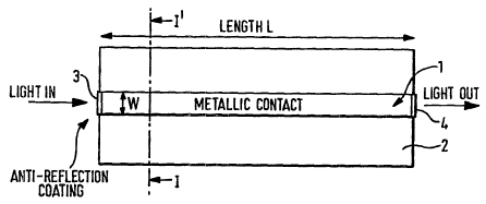
A. typical semiconductor optical amplifier A1 is shown in Figures 1 and 2
which is fabricated in the InGaAsP material system for use in
25 tfleco~ irqtion ~y~L~ S, with Wd~ h~ centred on 1.55 ,um. The
d~evice consists of an elongate qmp!ifirq~ion region 1 forrned on a substrate 2.The amplifirqtioll region 1 has an input 3 at one end for optical radiation and
an optical output 4 at the other end each formed with anti-reflection COd~;n~
A typical reflc~L;v;Ly is of the order of 10-3 ~ 10~. The input 3 and output 4
30 are COnL~ cd tO couple into single mode optical w~ u;des e.g. optical fibres
or ~ ly other structures (not shown) in~g~d~ed onto the substrate.
The region 1, as explained hereinafter is ~longqt~ with a length L and a
CA 02221693 1997-11-20
WO 96/41405 PCT/GB96/01376
-8-
and a width W defined by a lateral co.~;.. l structure. As will be
PYrlqinP~l her~drLcr, the length L of the amplifier region 1 is sPlPctef~ to be
longer than hitherto in order to i~Llluvc the amplifier cha d~ ;aLiCS. The
width W of the region 1 is sPlPctPcl for guided travelling wave operation and is5 typically of the order of 1-2 ~Lm, less than 50 ~m and usually less than 5 ~m.
The active amplifi~qtion region 1 can be fabricated in a ~ her of d;Lr~,~nc
ways _nd an example that cGl~ly~;ses a buried heterostructure is shown in
Figures 1 _nd 2. Referring to Figure 2, the active region 1, which produces
~o amplifir~tion, COl~ ~ a stack of multiple~l~ntllm-wells comprising a
plurality of alternate layers of InGaAsP-InP 5 formed on a n-InP substrate 6.
The active region 5 is overlaid by a p-InP region 7 formed with a conductive
over-contact 8 formed of p-InGaAsP material, provided with a mPtqlli~ contact
9. A mPtqlli~tion layer 12 is formed in the underside of the substrate 2.
~5
When forming the device, regions to the side of the elongate active region 1
arc IC~O~C;l by selea;ve etching in a m_nner known pcr se and layers 10 _nd
11 of p-InP and n-InP material are grown back.
20 Thus, the MQW stack 5 is sandwiched between p-InP region 7 and n-InP
layer 6 so that when a voltage is applied be.w_en the mPt~llir contaa 9 and
the mPt~ tion layer 12, an electric current passes through the stack 5. The
~.. ~... l of the n and p doped layers 10 and 11 forms a reverse-biased
junaion so that the current produced by the voltage applied to contact 9 is
25 directed sele_~;vely through the active region 1 rather than to each side, toprovide lateral cc.. r;.. r.ll Thus, photons inri~ent on input 3 ~Figure 1)cause ele~ ~rOllS to L.dvc.ae the b~n~ r of the MQW stack 5 so as to generate
a ~ rio~l photons, thereby producing optical amplifir~tion. For further
details of the structure of the device and various mo~ifir tions thereof,
30 reference is d;~e_~cd to "Long W~vele.l~;~L Semiror~ aQr Laser" Agrawal and
Dutta, ss~a, from which it will be s~rc_;,~cd that a bulk device can be used
as an ~ c.
CA 02221693 1997-11-20
W O 96/41405 PCT/~L~ 1376
_ 9 _
A s~....ro..~.lrtor optical ~mrlifi~r can be used as an active co...po~ in a
mo~lll -tQr as will be eA~ cd with reference to Figure 3. An e~ lly
co..~ .o..c target wave source 13 e.g. a laser opeldLlilg in the aforesaid optical
t~ tiQnc wd~dcn~,-L band, is directed into the input 3 of the active
region 1 of the amplifier. Also, an optical source 14, which has been
m~ tecl ~t a given bit rate is directed to the input 3 of the arnplifier. The
"1" bits of the mndlll~tion produce saturation effects in the active region witha result that the target wave becomes mn~ tecl by the signals from the
source 14 and the reC..lting output at output 4 comprises the target wave
Jo mn~nl~te~l with the mo~lnl~rion pattern from source 14. The target wave
source 13 and the mo~ t~c~ source 14 can operate at different frequencies so
that a w~velength conversion takes place. This process is known as cross gain
mo~ tion. As previously explained, the modulation may also produce a
phase change, which can be c~ctecte~ by comparing the pha~se of the
modulated output target wave with the phase of the input target wave from
source 13 (by means not shown).
In order to operate as a practical device, the modulator neets to be able to
operate over a wide range of bit rates for the moc~ t~ source 14. Thus, the
amplifier gain should not vary signifi~ ~ntly over the desired operating range of
bit rate mr r3lll~tion.
In accol.L.ce with the invention, it has been appreciated that this gain
bandwidth of the amplifier in respect of the mo~ tion bit rate is a function
of the length L of the optical active region shown in Figure 1. A derivation
of the w,~ ;Lll cc"~ on frequency l~J~onse will now be given in order
to show the length ~ep~on.l~r~ of the bandwidth chara. L~.;S~;CS. This is
car~ied out by firstly conci~l~ring the response of the arnplifier to a single
input beam and then eYtonrling the analysis to two input bearns by
Sllp~-~G';I;O~
Conci~ ;..g firstly the c~se of a saturated ~mplifirr with a single optical input
CA 02221693 1997-11-20
W O 96/41405 PCT/~L3~1~1376
- 10 -
beam, the carrier density N in the amplifier evolves with time as:
~ N = J _ R(N~ _ ar (N N~) p
where R~N) is the spontaneous recombination rate, J the injecred current
density, d the active layer thirkn~ss, e the electronic charge, A the active cross
5 section, r the mode confinlom~nr, hv is the photon energy, a is the material
gain, N~ is the transparency carrier density and P is the optical power.
This is known as self gain modulation and a fuller explanation is given in:
G. P. Agrawal & N. A. Olsson, "Self-phase modulation and spectral
~o broa~l.oning of optical pulses in semiconductor laser amplifiers" J. Q~l~nrum Electron., 25, pp 2297-2306, (1989).
It can be shown that the travelling wave equation for the optical power is:
(~ Z V8 ~--t) P= lar (N-N.)-~sclP(z) Iy
15 where CY5c is the waveguide loss per unit length. In the small signal regime, the zero-mean time-varying parts of P and N are denoted by ~P and ~N
~spe~iv.ly. The carrier density is then given by:
~N- -ar (N-N~ P/Ahv
i~(l/~c~arPO IAhv)
For a saturated amplifier, the gain becomes close to the w~v~;~,uide loss, and
20 the optical power becomes constant at a saturation value. The ~I.JpdE,,~lio~
equation (2) then beeolll.s, ignoring the phase factor:
LlL~gl~Llng this over the length L of the amplifier gives:
SUBSTllVTE SHEET (RULE 26)
CA 02221693 1997-11-20
W O 96/41405 PCT/GB96/01376
~p (elr )2(N-N~)Po /Ahv ~p
Z i~ TC~ar PO /Ahv)
~ PO = T (~) ~PfO)
where T(~) is a L~ srt- function defines as follows:
T( ) (ar )2(N-N~)Po /AhV L ~5y
i~t(V~c~ar po /Ahv)
Writing the stim~ te~l carrier lifetime as:
s ar P
and writing the optical gain as g e cxr ~I-NJ it follows that:
P i~l/TC~ s
o The analysis for a single input optical beam for the amplifier can be P~rten~Pby superposition to a cit~l,7tion where two beams of d;rr~ .l. w~. lf ..~ c are
fedl into the amplifier, in order to characterise cross modulation effects. Thiswill now be explained with reference to Figure 4.
15 In Fig,ure 4, two dir~.e.lL wi~ length input optical beams I, II of .e~e~L;vc powers Pl and P2 are shown for optical amplifier A, with the beam I
co~ , the mo~ ting bearn and beam II co..~ .l ;..g the tar~et beam.
SUBSTtTUTE SHE~Ell ~RULE 26)
CA 02221693 1997-11-20
W O 96/41405 PCT/GB96/01376
-12-
In Figure 4A, the cin- tior~ is conc;~lered where each input beam is illlp~ d
with a m~ tion pulse ~ so that input pulses ~ and ~ /r are applied to
the amplifier, as shown. The amplifier is O~..d~iVC SO that both inputs are
. I.~.~gr~ in proportion and so the inputs are amplified according to the
5 ~af~r function T(~) of the amplifier, which results in Ou~u~a ô.T(c~) and
.T(~)/r for the output beams.
In Figure 4B, a different situation is shown in which the input beams are
mod~ nor~ to produce inputs +~ /r and ô /r respc~Liv~ly. The amplifier is
o operated so that the input (and output) power is kept constant so that the
OuL~uLa are the same as the inputs i.e. +ô /r and ~/r.
Figure 4C shows a superposition of the inputs and Ou~puLS of Figures 3A and
3B. By considering the relationship between the values of the input and the
~5 OuLyuLa shown in Figure 4C and s~ksL;l~ll;..g for r, it can be shown that the cross gain modulation response TXGU(~I~) is given by:
T~)= ~ T(~-l) O
The bandwidth of wd~lcll~Lh conversion through cross gain modulation as20 given by equation (8) is found, in accordance with the invention, to increasealmost linearly with amplifier length. The 3db limit for the bandwidth of this
~on~ ,;on can be understood by further analysis of terms of equation (8). It
will be understood that for a given operational condition the term Pl/ Pl+P2
is a CC~llaL~lL but that the term CI (~)-1) is variable in both frequency and
25 phase, and has both real and i~ g;~ y parts. Figure 5 shows a plot of the real
and i...ag;.~.y parts of the function F ; (T(cl~)-1) on orthogonal z and y axes.For inclca ill~, frequency, the function F describes a widening spiral 15
beginning at near z--1 for ~-0, and finiching at z-O for ~- ~. Stated
c~lLly~ the f~ln~rion T(~) spirals ouLwdrdly from the point (-1,0) to the
CA 02221693 1997-11-20
W O 96/~1405 PCT/GB96/01376 -13 -
point (0,0). The 3db w~.~clengLh conversion bandwidth limit for function F is
described by the locus 16 of a vector of mo~ c 0.5 centred on the origin and
is encou~l~cl~d when the wirlening spiral 15 crosses the arc 16. By plotting
the real and i.,.~;n-~..y parts of F for different values of gL, it has been found
5 tha1: when the spiral 15 crosses the arc 16, the phase angle for the c~ s~;on
T(~) is always close to ~r/6. Thus by equating the ph~se of T(~) in equation
(7) ro ~/6 ~ a frequency corlrlirion ~db for the 3db bandwidth to be to
be ~ ~y.~sed as follows, m-king the assumption that the arnplifier is O~..dt;llgin a s~turated condition i.e. the srim~ t~c~ carrier lifPtimP ~s is smaller thano the spontaneous lifPtim~ ~c:
3gL
~3d~
Thus, it can be seen from eq~rior- (9) that the 3 dl3 bandwidth is
a~pro~ ely linearly dependent on to the length L of the arnplifier when
other factors such as injection curren~ density are m~int~in~pf~collsLallt.
~5
This effect can be seen from the experimPnr~l set up that will now be
described with reference to Figure 6. The target wave source 13 comprises a
DFl3 laser operating at 1.555 ~m, and the morl~ terl source 14 comprises a
tunable laser 14a Op~-d~illg at 1.560 ~m, that feeds radiation to a Mach-
20 ~Phn~Pr ~M-Z) morl~ ror 14b. The OU~puLS of both arnplifiers are fed
through ..~pe-,~ivl: erbium doped fi~re arnplifiers 17, 18 and associated
polaLrisation controllers 19, 20 2~tPnll~tors 21, 22 and filters 23, 24. The
r~s..lring m~ te~ signal ant target wave are combined by a 3 db coupler 25
and fed into a first serniconductor arnplifier A1 having an active region of
25 length L, which is r~c~arl~p~l to a second serniconductor optical amplifier A2
with an active region, also of length L. The arnplifiers are connpc~er~ in series
with optical isolators 26A, 26B, 26C for suppressing ASE. The rrclllting
outE~ult is fed through a further filter 27 and an ~ Qr 28 to a tetector
diodle 29, which feeds an ~IP~ signal through a PlPcrric~l ~mplifiPr 30 to a
SUBSmUTE SHIEET (RULE 26)
CA 02221693 1997-11-20
W O 96/41405 PCT/GB96/01376
.._Lwurk analyser 31. The analyser 31 also provides ele_~;~l control signals
to the mo~ or 14b. The mr~ ?r 14b was swept through a bit rate of 300
Mhz to 40 GHz. The responses were measured for three d;rr~.en~ cases: with
only the amplifier Al, with only amplifier A2 and also with both amplifiers
5 ~cr.rl~rl The amplifiers used were both of length L 1.125 mm with a
ccil.c ~ width W of the order of 1 micron, and a gain peak at 1.550 ~m.
The signal and target powers injectecl into the amplifiers were +2.5 and -1.8
dBm rc~.~e_Li~ly which resulted in the gain being saturated and the Fabry-
Perot ripple being reduoed to below .5dB. The drive current to each amplifier
o was set at 140 mA and the single amplifier XGM bandwidth was below 10
GHz.
The results obtained are shown in Pigure 7. Traoe 32 shows the gain of the
amplifier as a function of frequency for a single amplifier, whereas traoe 33
~5 shows a result for the two amplifiers active regions lA, lB r cca~ It can
be seen from Figure 5 the -3db bandwidth for a single amplifier, of 6.5 GHz
is increased to over 13 GHz when two arnplifiers are ~cc7~P~ This is
attributed to the fact that the length L through the r~cra~lec~ amplifiers is
increased, in this example to 2.25 mm by connPrting the two amplifiers in
20 senes.
Figure 8 shows an arr~ngPmpnt in which the r~Cc~e~ amplifiers have their
drive current increased from 140 mA as described above, to 400 and 500 mA
r~e_~i~ ely. The reslllting bandwidth exhibits a -3db roll off at 28 GHz,
25 Sll~S~ lly greater than hitherto.
It will be ~ L d that the c~c~ing of two amplifiers produoes s~lb~
losses at the junctions between them and so by forming a single amplifier of
lengh that exceeds 1 mm, a s.lhst-nti-lly h~pr~v~ d bandwidth can be
30 provided, that extends beyond 20 GHz bit m~ tion rate for amplifier drive
~.U~C~L5 --400 mA.
CA 02221693 1997-11-20
W O 96/41405 PCTtGB96/01376
- 15 -
Typic~ of the length L of a single sPmil-Qn~ Qr optical amplifier
are in excess of 1.00 mm, 1.125 _m,1.25 mm, 1.5 mrn, 1.75 mm, 2.00 mm,
2.20 mm, 2.25 mm, 2.50 mm or 2.75 mm, with a drive current adjusted to
achieve a current density in the acsive region of typically 50kA/cm2. The
5 driv~ current may be ~ e~3 to achieve a -3 db w~ ngLh co~ ;on
bandwidth that PYtPn~lC beyond 28 GHz or 35 GHz or 40 GHz. the width W
is typically of the order of 1-2 ~m, less than 50 ~m and usually less than 5 ~m
Alte~lla~;v.ly, a ntlmhPr of devices may be r~c~ .1 as described in order to
~o achieve the desired path length, with isolators between them in order to
au~ c~s ASE.
In these exarnples, an amplifier with a MQW structure is used, in which case a
patb length at least in excess of 1 mm is provided for a l~h~nnPl width W of
~5 less than 5,um. However, as previously explained, bulk devices can
all.e~ cly be used, in which case the path length can be shorter, typically
in excess of 800 rnicrons, because of the higher effi~-ncy of bulk devices
compared with MQW devices.
20 R.~f~..mg now to Figure 9, this shows the -3db bandwidth (plot 34) and peak
frcquency (plot 35) for the w.~velength cc~ a;on as a function of arnplifier
length. It can be seen that both chala~.;a~;cs have a linear relationship with
the Length of the active region of the amplifier. The arnplifiers used to obtainthe data were constructed as described with reference to Figs. 1 and 2 and
25 were of the same construction apart from the length of their active region.
They were ope...Led under the same c~ntlitions.
A ty pical practical ~arnple of the device may be constructed as described with
re~erence to Figs 1 and 2 with an active region 1 of lengtlh L - 3.5 rnrn and
30 width W - 1- 2 ~m,with the depth of the layers in the collLilet active
region being of the order of 0.1- 0.2 ~m. This can be op_.dLed with a
w.~ co~ a;on bandwidth of the order of 40Gb/s, with a typical drive
CA 02221693 1997-11-20
W O 96/41405 PCT/GB96/01376
-16-
current in thc range of 500 mA to 2000 mA. .
A practical example of the invention will now be described with reference to
Figure 10. A serniconductor optical amplifier in accord~ce with the
5 invention, as previously described, is used as a wdv.le.lgLh con~c,L~,. Optical
digital commllnir~tirJn signals from a motllll~tPcl source 14 at wd~.l.ngLh ~0
are ~dpplied to the co.~ ., which inr~ Pc an optical arnplifier with an
active region 1, as previously described, with a length L - 3.5 mm. A target
wave source 13, which is tunable in terms of W'dv~ h, is also applied to the
o wavelength converter. A nllmher of output rh~nnPlc are conn~cte~ to the
output 4 of the amplifier, which are typically conctitl~te~3 by optical fibres F1-
F4 connPctecl to dirfc~cn- geo~,-dphic ~IPstin~tions. Each fibre has an
~cSori lte~l band pass filter 35, 36, 37, 38 tuned to a particular wavelength ~
The target wave source 13 is Nnable to the individual wavPlPngthc ~ , 50
IS that by setting the target wave source wdvrlP.~Lh, the mo~ tirJn from source
14 can be converted to the w~ le~ h of the target wave source and
con3~luently direaed to a s--lPcted individual one of the commnnir~tion
rh~nn~lc
20 An alte..l,~ive use of an amplifier according to the invention is as a time
~Pmllltirlexer, in which data configured in interleaved time slots are separatedinto different rh~nnPlc Rer~ g to Figure 11, s~lc~ ;ve data time slots
S1...SN contain data denoted by the presenoe or ~l.senre of optical pulses. The
time slots are interleaved and are to be directed to d;LL,~ rh~nnPlc Chl,
25 Ch2 ~w~e~ .ly by a ~lPmllltirlpypr DM1. A suitable structure for the
~lemllltirlexer DM1 is shown in Figure 12.
The ~IPmllltirlexer DM1 co l~,.;ses a Mach-7Phn~er loop structure inrhl~ling
first and second optical fibres 39,40 with two coupling regions 41, 42. As well
30 known in the art, for a Mach-7Phn~P~ loop structure, an optical output is
produced at the output OP1 or OP2 ~epPnt~ing on the relative phase of the
signals travelling in the portions 43,44 of the fibre loop. In accordance with
CA 02221693 1997-11-20
WO9'6/41405 PCT/GB96/01376
the invention, . n optical amplifier A1, co~L. u~L~d as previously r4~rrihe~l~
with an active region of length > 1.25mm, is connrctP~ in one of the loops so
as tO control the relative phases of signals in the portions 43,44 of the loop
and direct signals to the ou~u~ OPl, OP2 sele~L;~,~lr.
s
The ~e.lea~cd optical data stream for both C'hqnn~lc 1 and 2 from source 14
is fcd to input IP1, whereas a control optical pulse strearn is fed to the inputIP2 from source 13. The control pulse strearn includes pulses which ~l~olin~
in time, data slots for C~h~nn~l 1. The signal ~Llcd~s fed to the inputs IP1,2
ro are of .~._L;~e d;rf~.c.lL wav~lPn~hc or polaricqtionc, or both and are mixedtogether by the coupler so that the mixed strearn travels along both fibre
portions 43,44. The arnplifier A1 produces a phase shift in the signal strearn
travelling in fibre portion 43 relative tO portion 44 as a result of cross phasemr.~lllqtion that occurs in the amplifier during the occurrence of the control
pulses that occur for the data slots for (~hqnnPI 1, and as a result, optical data
pulses for Ch~nn~l 1 are directed scle~lively to OP1 whereas data pulses for
(~Ih nnPl 2 pa s to output OP2. It will be understood that either C'.h~nn~ l 1 or
2 may itself include a plurality of further rh~nn~lc that can bé separated by
m~esns of additional ~lemllltirlexers.
Whilst the described Mach-7~hrl~er device has been tescribed for use ac a
~m~ull ;l.e..~r, it can also be used as a switch for other applil~rionc e.g. forrouting packets in packet switched networks, for gating signals for other
purposes and for il~rvv;llg the PYrinc~ion ratio of a digitally rno~ t~d
25 optical signal.
Mach-7~ nrl~r loop structures will now be described, that
incorporate optical arnplifiers A1, A2 in both of the portions 43, 44 of the
fibre loop, with both of the arnplifiers being constructed as previously
30 ~lecrTjhl?d e.g. each with an active region of a length greater than 1.75 mrn.
In Figure 13, the optical path length from the splitter ~.1 tO each of the
CA 02221693 1997-11-20
W O 96/41405 PCT/~L3G~'~1376
-18-
qmplifiPrs A1, A2 differ by an offset d. Thus, conci~ ng the inputs IP1 _nd
IP2, the input signals reach the a{nplifier Al before the amplifier A2, with theresult that a very narrow switching window is pro~..oe~; useful for
~mllltiplexing. The use of amplifiers A1, A2 in accor~ce with the
5 invention, sharpens the ~Pfinition of the switching window and so enables
shorter switching windows to be achieved thqn hitherto. In this
configuration, the width of the switching window is fixed by the spatial offset
d, during the fabrication prooess for the devioe.
o Referring to Figure 14, an alternative configuration is shown in which the
amplifiers Al and A2 are disposed symrnetrically in the inte.r..~ eter but the
control signal IP2 is fed into the portion 43 of the loop through a separate
coupler 46 so that for exarnple, dPmllltiplexing can be carried out in the
manner described with reference to Figure 12. However, the presence of the
15 ~yllull~Li;cal disposition of the arnplifiers Al, A2 enables mqtching of losses in
both portions 43, 44 of the fibre loop. The use of the longer amplifiers Al,
A2 in accordance with the invention enables the phase rhqnges that occur in
amplifier Al to be speeded up as colllp.u~d with the prior art.
20 In Figure 15, the amplifiers Al, A2 are disposed syrnrnetrically in the
inte.r~,~,rllc.er and control signals can be injectec~ into the amplifier inputsindividually through i~L,e~ive optical coupk.~ 46, 47. In the example
shown, the input IP2 is fed into both of the couplers 46, 47, with the input to
coupler 47 being delayed in time relative to the input for coupler 46. As a
25 result, a very narrow switching window is produoed in the manner described
with reference to Figure 13. The use of amplifiers in accordance with the
invention can sharpen the ~w;~ Li~lg window. In the collr;l ur~;on of Figure
15, the delay be.w.~.~ the two injected control signals IP2, IP2 + ~ can be
varied so as to adjust the length of the switching window.
The invention also has application tO s~mic-onrll~ctor optical arnplifiers whichare used in moc~ tors that operate by four wave milring. It h~s been found
CA 02221693 1997-11-20
WO 96/41405 PCT/GB96/01376~ - 19 -
according to the invention that by in._.~as;llg the length of the amplifier, the~ffiriPr~y of four wave mixing is h~lpl~v~d ant the signal to noise ratio is
incrleased. This will now be explained by way of example with reference to
Figures 6 and 16. The appaldL~Is of Figure 6 was driven such that the target
wave xource 13 operated at relatively high power and provided a pump for the
amplifiers A1, A2, and a pul.lpil1g wd~lcn~,~h ~ p - 1.55~ ~Lm. The
tunabl.e laser 14a was O~..dLCrl at a w~ h of ?~2 - ~i ~ 1.560 ~m. The
ou~,u~s of the lasers were applied with the sarne polarisation to the arnplifiers
A1, A2. The amplitude of the output of laser 14a was cignifir~ntiy lower
o than that of laser 13 with the result that four wave n~ixing occurred as can be
seen. from Figure 16. A w~v~le,lgth converted signal ~c was produced. The
wavelength relationship between the signals is as follows:
~c ~- 2 ~p ~
~5
Thus, the converted signal and the input signal are equally spaced in terms of
wav. l~ n~Lh on GppO~ e sides of the purnp wd~lc~ h ~p as shown in Figure
16.
20 A rion-limiting, qualitative explanation of the four wave n~ixing process will
now be given. Due to the fact that )~p and ~\i are of the sarne polarisation,
they form a beat frequency of the order of 100 GHz which causes the carrier
density in the amplifiers to osrill~te This produces a non-linear effect in
respect of the gain, which produces funther beating with the pump wd~ele~ h
25 SO as ltO produce the wd~ Lh collv~.Led signal ~c. For further details,
reference is directed to Stubkjaer et al s~a.
The e~fect of o~L.d~;ng the ~pald~us of Pigure 6 with only one of the
ampli~iers A1, A2, and then with both of the amplifiers is shown by a thick
trace 48 and a thin trace 49 rL.~ ~Liv~:ly. It will be seen that the four wave
mLYiQg conversion e~iri~ncy il~ro~ with increased amp~fier length L.
SUBSTITUTE !;HEET (RULE 26)
CA 02221693 1997-11-20
W O 96/41405 PCT/G B96/01376
- 20 -
amplitude of the CO..~._,LC;I signal ~c nl~ ,LSes. Also, the signal to noise ratio
iS iLU~I~u~_d. It will be seen that the noise floor 48a of trace 49 is ~u~.~.d
duwl~w~dly as colll~cd with coll~s~onding floor 48a when a single
:ImplifiPr is used so that the signal to noise ratio is increaset, in respect of the
5 coll~,~.Lcd signal ~c . It is to be noted that the ~u~lession of the noise floor
occurs asy~ , ;e~lly~ and the w~le~ collvclLed signal ~c is pocitio~
on the d~lu~ Le side of the pump wd~lcngth ~p to take advantage of th
asylll~lcLl;cal~ d~wllwald ~ that occur tû the noise floor.
o As previously mPntion~cl four wave mixing has the adv~tagc that the
WdV. 1L~1~;L11 collv~- ,;on occurs rapidly as compared with cross gain
m(~ ti~ln. The convc.Led signal ~\c can be imparted with a modulation, by
mo~ ting the input signal ~j. This can be achieved in the configura~ion of
Figure 6 by o~.ldLmg the mr.~ tor 14b.
An amplifier that uses four wave milring, can be used to correct dispersion in
a signal travelling along an optical rommlmi~tion path e.g. a signal travelling
over long ~ict~nres The signal travelling along the path may be subject to a
frcquency shift due to the di~pela;vc effects of the path e.g. an optical fibre.20 An amplifier which operates by four wave rnixing can be used to change the
wdvel~ ;Lh of the input signal )~; to ~c to achieve an inversion of the signal
w~v~le,l~;Lh relative to ~p, so as to ccl~ nsdLe for chirp
It has been found that for four wave mi~ing, the ~ffir;.-ncy of the amplifier is25 ~lux;~ fly proportional to the square of its path length i.e. E--L2.