Note: Descriptions are shown in the official language in which they were submitted.
CA 02221723 1997~ 20
OPTICAL CARD
BACKGROUND OF THE INVENTION
The invention relates to an optical card capable of
optical information recording, and technology for producing
it.
An optical card has been known as a memory card
incorporating an optical recording zone, i.e., an optical
information recording zone, in a plastic card. Fig. 1
shows an example of a WORM ( write-once/read-many) type
optical card. In an optical recording zone 2 of this
optical card 1, track guides 4 and information recording
pits 5, each composed of a low reflectance area, are formed
as preformats along with high reflectance areas. Among
optical cards of this type is an optical card whose low
reflectance areas are composed of light scattering surface
roughened portions. Such an optical card has been proposed
as a product using an optical recording medium whose
manufacturing process is relatively simple, whose material
is not restricted to a particular optical recording
material, and whose production cost is low enough to be
suitable for mass reproduction on a commercial scale (see,
for example, Japanese Patent Publication No. 64141/95).
The production of this optical card begins with the
preparation of a surface-roughened original plate having
low reflectance areas surface roughened according to an
information record pattern. The resulting original plate
is duplicated and transferred to mass produce the optical
card having a rough surface information record pattern.
The steps for its manufacturing process will be
described with reference to the accompanying drawings.
At a first stage, a positive photoresist is uniformly
coated on a transparent substrate 11 (a 400 ,um thick
acrylic plate) to a thickness of 0.5 ,um by means of a
rotary photoresist coater to form a photoresist layer 12,
CA 02221723 1997~ 20
as shown in Fig. 2A. At a second stage as shown in Fig.
2B, a photomask 13 formed in accordance with an information
record pattern is superimposed on the photoresist layer 12
using a mask aligner, and then initial exposure (patterning
exposure) is performed. At a third stage as shown in Fig.
2C, a glass sheet 14 roughened on one surface in a finely
- uneven form (average roughness 0.3 ,um, #3000 abrasive
glass) is used, and exposure is performed again (surface
roughening exposure). After exposure, the photoresist
layer 12 is developed at a fourth stage. Thus, as shown
in Fig. 2D, the pattern of the photomask 13 is transferred
onto the transparent substrate 11, with the exposed areas
of the photoresist being dissolved and the unexposed areas
remaining. By this measure, the surface roughened
photoresist layer 12 is formed as guide tracks, for
example, with a width of about 2.5 ,um and a pitch of about
15 ,um.
Then, an optical recording medium having an information
record pattern composed of low reflectance areas roughened
on the surface (a medium as shown in Fig. 2D) is used as
a surface roughened original plate 15. From this surface
roughened original plate 15, a mother mask is duplicated
using a molding press. Specifically, as shown in Fig. 3A,
the surface roughened original plate 15 is superimposed on
a transparent substrate 21 (an acrylic plate 12 mm in
thickness) via an impression material 22 comprising a
molding compound of an ionizing radiation curable resin or
a thermosetting resin. The combination is pressed, and
then the surface roughened original plate 15 is stripped
to duplicate a pattern on the transparent substrate 21
side, thus forming a mother mask 23.
Then, the mother mask 23 is used as a duplicating
original plate for mass duplication, and impression using
it is performed to duplicate an optical recording medium
on the back of a substrate serving as a transparent
protective layer of an optical card. In detail, as shown
in Fig. 4A, a molding resin 33 is interposed between the
CA 02221723 1997~ 20
back of a transparent protective layer 32 having a surface
hardening layer 31 and the pattern surface of a mother mask
23. The assembly is pressed by a pressing machine to
undergo hardening. Then, as shown in Fig. 4B, the trans-
parent protective layer 32 and the mother mask 23 arereleased from the mold to duplicate a pattern on the
transparent protective layer 32 side. In this manner, high
reflectance areas 33a and low reflectance areas 33b are
formed on the duplicating resin 33 to serve as an optically
transparent substrate for an optical card.
Then, as shown in Fig. 5, an optical recording material
layer 34 of, say, the intermediate oxide of Te, is laminat-
ed to cover the high reflectance areas 33a and low reflect-
ance areas 33b in the optically transparent substrate
composed of the duplicating resin 33.
Separately from the foregoing series of steps, a card
substrate 35 as shown in Fig. 6 is prepared. This card
substrate is formed by applying a print layer 36 to one
surface of a core sheet 35b comprising translucent polyvi-
nyl chloride, and bonding overlay sheets 35a, 35c compris-
ing transparent polyvinyl chloride to both surfaces of the
core sheet 35b.
Then, the card substrate 35 is adhesion laminated to
the substrate having the optical recording material layer
34 via an adhesive layer 37 comprising urethane resin, as
shown in Fig. 7. The so prepared master is punched into
a card form to produce an optical card as illustrated in
Fig. 1.
The aforementioned production of a conventional surface
roughened original plate posed the problem that the
resulting roughened surface contained defective areas
because of the processing method during production, the
limits of the properties of the materials used, and slight
changes in the manufacturing conditions. In extreme cases,
the resulting original plate partially had no sufficiently
low reflectance. Optical cards duplicated from such an
original plate were not entirely satisfactory in the
CA 02221723 1997-11 20
contrast of the preformat portions.
DISCLOSURE OF THE INVENTION
The present invention has been accomplished in the
light of the above-described problems. Its object is to
provide an optical card having a preformat portion compris-
- ing a low reflectance area having a satisfactory contrast
to a high reflectance area.
To attain this object, the optical card of the present
invention is an optical card having a preformat portion
comprising a low reflectance area, wherein the low reflect-
ance area comprises stereostructures comprising pyramidal
convexes or inverted pyramidal concavities.
Furthermore, an optical card original plate of the
invention for use in the production of the above optical
card is an original plate for duplicating an optical card
substrate bearing an optical recording material layer,
wherein the portion corresponding to a preformat portion
of an optical card each have a stereostructure (three-
dimensional structure) in a pyramidal shape or an invertedpyramidal shape. That is, those portion of the invention
each do not show a low reflection pattern by light scatter-
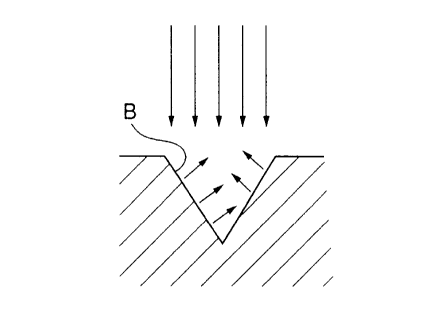
ing on a conventional roughened surface A as shown in Fig.
8. Instead, those portions each have a stereostructure B
in the shape of an inverted pyramid as shown in Fig. 9.
This structure forms a pit pattern in which the surfaces
constituting a three-dimensional object comprise mirror
surfaces having a particular angle. Because of this
pattern, this structure reflects incident light in specific
directions other than the direction of incidence. Thus,
an excellent contrast in an optical card optical system can
effectively be obtained.
BRIEF DESCRIPTION OF THE DRAWINGS
Fig. 1 is an outside drawing showing an example of a
WORM type optical card;
Figs. 2A to 2D show a process drawing for the prepara-
CA 02221723 1997-11-20
tion of a surface roughened original plate by a convention-
al method;
Figs. 3A and 3B show a process drawing for the prepara-
tion of a mother mask from a surface roughened original
plate;
Figs. 4A and 4B show a process drawing for duplication
of an optical recording medium on the back of a substrate
which serves as a transparent protective layer;
Fig. 5 is a sectional view showing the lamination of
an optical recording material layer on a part of an
optically transparent substrate;
Fig. 6 is a sectional view of a card substrate;
Fig. 7 is a sectional view showing a state in which a
card substrate is adhesion laminated to an optically
transparent substrate bearing an optical recording material
layer via an adhesive layer;
Fig. 8 is a sectional view showing light scattering in
a conventional surface roughened pit;
Fig. 9 is a sectional view showing a low reflection
pattern by an inverted pyramid-shaped stereostructure;
Figs. lOA to lOG are collectively a process drawing
showing a method for producing an optical card original
plate relevant to the present invention;
Figs. llA and llB are views showing concrete examples
of a pyramidal shape;
Figs. 12A and 12B are views showing concrete examples
of an inverted pyramidal shape; and
Figs. 13A and 13B are the waveforms of read signals in
the preformat portions of optical cards related to the
present invention and the prior art, respectively.
BEST MODE FOR CARRYING OUT THE INVENTION
An optical card original plate for use in the produc-
tion of the optical card of the present invention will be
described, including a method for preparing it.
An optical card original plate according to the present
invention is an original plate for duplicating an optical
CA 02221723 1997-11-20
card substrate bearing an optical recording material layer,
wherein the portions corresponding to preformat portions
of an optical card each have a stereostructure in an
inverted pyramidal shape. This inverted pyramid-shaped
stereostructure can be formed by the anisotropic etching
of a single crystal substrate. Generally, when a single
crystal silicon substrate is anisotropically etched with
an alkali, the etching rate is high on the (lOO) plane and
low on the {111} plane in terms of the Miller indices of
the crystal. Assume here that a substrate having the plane
of etching comprising the (lO0) plane is used as generally
done in semiconductor fabrication, and this substrate is
etched such that the longer-dimension side of a pattern to
be etched will be parallel to the <110> plane. In this
case, an inverted pyramidal structure comprising four
surfaces defined by {111} is automatically formed.
Moreover, a resin original plate for an optical card
regarding the invention is obtained by duplication from the
above-mentioned optical card original plate by use of a
molding resin. Furthermore, a stamper can be formed by
duplication from the resulting resin original plate with
the use of a molding resin.
An optical card according to the invention which is
obtained using the above optical card resin original plate
or stamper has preformat portions comprising low reflect-
ance areas for light, the low reflectance areas being
composed of pyramid-shaped or inverted pyramid-shaped
stereostructures. That is, the aforementioned inverted
pyramid-shaped structures produced by the above-
mentioned anisotropic etching of a single crystal substrate
are utilized as the preformat portions of the optical card,
whereby low reflectance preformat portions free from
defects and surface unevenness can be formed easily and
rapidly.
Such a structure is different from a simple V-groove
structure which has been studied in a conventional
disk-shaped optical disk or the like. The above structure
CA 02221723 1997-11-20
is a pyramidal structure having an inclination also on a
plane perpendicular to the direction of scan by an optical
pickup. This prevents abnormal reflection of light at the
edge of the preformated pit in the scan direction. Thus,
S read errors for readouts in the pit edge recording method,
in particular, can be reduced or prevented. In addition,
this pyramidal structure is completely geometrical, so that
its inspection and management are easier than conventional
surface roughened pits comprising irregular convexes and
concavities. Thus, the yield of the resulting product can
be increased.
The above-mentioned pyramidal shape (convex state) in
the present invention includes the shape of a hipped roof
as shown in Fig. llB in addition to a quadrangular pyramid
as illustrated in Fig. llA. Whereas the inverted pyramidal
shape in the present invention includes the shape of an
inverted hipped roof as shown in Fig. 12B in addition to
an inverted quadrangular pyramid as illustrated in Fig.
12A.
Figs. lOA to lOG are collectively a process drawing
showing the procedure for producing an optical card
original plate relevant to the present invention. Pre-
ferred embodiments of the invention will be described by
way of an explanation for this process drawing.
As shown in Fig. lOA, an etching protective film 42 was
formed by the customary method to a thickness of about 0.1
,um on a mirror polished (100) single crystal silicon
substrate 41 for semiconductor preparation. The etching
protective film 42 was composed of thermally oxidized
silicon dioxide which is used as a conventional semiconduc-
tor protecting film or element separating film. On the
etching protective film 42, a positive resist (AZ-5200,
Hoechst A.G.) was uniformly coated by rotary coating, and
heat-dried to form a resist layer 43 about 0.5 ,um in
thickness. The heat-drying treatment was performed for
about 20 minutes at 150~C using a hot plate.
CA 02221723 1997-11-20
Then, as shown in Fig. lOB, the resist layer 43 was
pattern drawn by an ionizing radiation exposure device or
a mask aligner in the customary manner. If an EB exposure
device is used, this drawing step is performed at an
accelerating voltage of 20 kev and an exposure of 10
~C/cm2. Then, the exposed resist layer 43 is dip developed
for 1 minute at room temperature in an aqueous solution of
an alkali developer consisting essentially of tetramethyl-
ammonium hydroxide, and rinsed with flowing deionized
water. In the case of one-operation transfer using a mask
aligner or the like, an exposure of 50 mJ/cm2 by a metal
halide lamp is used. Subsequent development and rinsing
steps are the same as in the above. By the above-described
process, the desired resist pattern was formed as shown in
Fig. lOC. Then, the composite was heat-treated for 30
minutes at 120~C in an oven to enhance the adhesion between
the resist layer 43 and the etching protective layer 42.
Then, as shown in Fig. lOD, the etching protective film
42 exposed to the outside through the opening of the
patterned resist layer 43 was removed by dry etching. The
dry etching was performed by a parallel planar electrode
type RIE dry etching device under the following conditions:
0.1 mTorr, CHF9-93 sccm, ~2-7 sccm and 0.2W/cm2. Before
etching of the etching protective film 42, a descumming
treatment with oxygen plasma is performed if desired. This
treatment is performed for 1 minute using the same etching
device under the conditions: 0.2 mTorr, O2-lOO sccm and
0. lW/cm2.
Then, as shown in Fig. lOE, the patterned resist layer
43 was peeled off with a solvent. The peeling was per-
formed ultrasonically for 3 minutes at 60~C using a peeling
solution consisting essentially of ethanolamine, and then
rinsed with deionized water. After peeling of the resist
layer 43, the substrate was washed by an ordinary washing
device for a semiconductor substrate.
Then, as shown in Fig. lOF, patterning of the single
CA 02221723 1997-11-20
crystal silicon substrate 41 was carried out by wet
etching. Concretely, the wet etching was performed for 3
minutes at 70CC using a 10 wt.~ aqueous solution of
potassium hydroxide. The amount of etching at this time
S was about 3 ,um. The etched product was rinsed with deion-
ized water, and dried.
Of importance here are the crystal orientation of the
single crystal silicon substrate 41 and the dimensions of
the pattern to be formed. Generally, when a single crystal
silicon substrate is anisotropically etched with an alkali,
the etching rate is high on the (lOO) plane and low on the
{111} plane in terms of the Miller indices of the crystal.
Also, the etching rate for a single crystal silicon
substrate depends on the impurity concentration of boron
contained in the crystal, and decreases as the boron
concentration increases. To obtain an inverted pyramidal
structure by the anisotropic etching of a single crystal
silicon substrate, therefore, it is vital to use an n-type
single crystal silicon substrate having the plane of
etching comprising the (lOO) plane as generally used in
semiconductor production, and make the longer-dimension
side of a pattern to be etched parallel to the <110> plane.
The etched side surface comprises the {111} plane.
Thus, to give an inverted pyramidal structure and avoid the
formation of a planar portion at the bottom of the etched
surface, the etching time needs to be about 1.5 times that
for the shorter-dimension of the etching pattern.
Finally, as shown in Fig. lOG, the patterned etching
protective film 42 is removed by dry etching if desired.
The dry etching is preferably performed under the same
conditions as those for the aforementioned etching of the
etching protective film 42 exposed to the outside. If
desired, a descumming treatment with oxygen plasma is
performed as a final treatment. The conditions for this
treatment are the same as stated previously. With this
treatment, the procedure for manufacture of an optical card
original plate is completed. The bottom angle a of each
CA 02221723 1997-11-20
of the two equal sides in the so obtained optical card
original plate shown in Fig. lOG was 54.7~C.
The succeeding procedure until the production of an
optical card may be the same as described earlier.
S A single crystal substrate is itself a relatively
expensive material. From the above optical card original
- plate comprising a single crystal substrate, therefore, a
replica may be duplicated using a molding resin for use in
the preparation of an optical card. This replica per se
may be used as a resin original plate for an optical card.
Furthermore, a replica duplicated from this resin original
plate by use of a molding resin may be used as a stamper
for an optical card.
The pyramidal structure may be concave or convex
lS relative to the transparent protective layer of the optical
card. In either case, the same effect is obtained. To
improve the duplication properties or plate wear of the
resin original plate, various suitable coating agents may
be applied to the duplicating surface.
A plurality of the above-described stampers are put
together to form a multi-plane stamper, whereby optical
card production can be made more efficient. An example of
the method for preparing such a multi-plane stamper is to
tie together a plurality of mother stampers to form a
multi-plane mother stamper, and use this multi-plane mother
stamper as a source of duplication to form a multi-plane
stamper. A preferred example of this multi-plane formation
will be described below.
A plurality of silicon wafers cut to about the size of
one surface of the desired optical card are arranged on a
substrate so as to have the same crystal orientation, and
they are fixed there. Then, the combination is molded
using resin or molten glass for integration. Thereafter,
the composite is polished until the surface of each of the
silicon wafers arranged on the substrate is exposed to the
outside. Then, a photosensitive material is coated
thereon, and a pattern is drawn in the coated assembly by
CA 02221723 1997-11-20
contact exposure through a multi-plane photomask or
directly by ionizing radiation. The patterned product is
etched to obtain a multi-plane original plate. From this
multi-plane original plate, a multi-plane stamper can be
S produced by the aforementioned method.
A comparison was made between the reader/writer output
signal waveforms in the preformat portions of the optical
card of the present invention obtained by the
above-described method and an optical card obtained by the
aforementioned conventional surface roughening method. The
results are shown in Fig. 13A (the invention) and Fig. 13B
(the conventional product). The waveforms indicated are
based on records of pit lengths. In the optical card of
the invention illustrated in Fig. 13A, the maximum ampli-
tude (1,370 mV) of the signal waveform is large and stable,showing no error signals. In the reader/writer output
signal waveform in the preformat portion of the optical
card obtained by the conventional surface roughening method
illustrated in Fig. 13B, the maximum amplitude is 1,170 mV,
showing an error signal exceeding the signal threshold
value at the portion indicated by an arrow.
The present invention has been described based on the
preferred embodiments. The method for preparation of the
original plate, etc. stated in the present specification
is intended for illustration only, and is not to be
restricted to the materials, devices or conditions used
there. The dry etching conditions, in particular, are
strongly affected by the etching apparatus, the structure
of the etching chamber and so on. The wet etching condi-
tions are also influenced by the etching area and theamount of the etching solution. Thus, these conditions are
not limited to the aforementioned conditions.
As described above, the optical card original plate of
the invention has not conventional surface roughened
structures, but inverted pyramid-shaped stereostructures
whose respective surfaces are mirror surfaces. Thus, the
original plate is defectless and free from surface rough-
CA 02221723 1997-11-20
nesses, and so ensures a sufficiently low reflectance. An
optical card produced from this optical card original plate
has preformat portions comprising low reflectance areas
with a satisfactory contrast to high reflectance areas.
S The manufacturing process for this optical card is differ-
ent from the manufacturing process for a conventional
optical card solely in the step of preparing the counter-
part of a surface roughened original plate. Thus, the
procedure of the invention is advantageous in that a
conventional duplication technique can be utilized as such
without making the process complicated.