Note: Descriptions are shown in the official language in which they were submitted.
CA 02221942 1997-11-21
[67190/954084]
INSULATING COMPONENT FOR HIGH-VOLTAGE EQUIPMENT
FIELD OF THE INVENTION
The present invention relates to an insulating component
for use in high-voltage switching equipment, and more
particularly for use in a gas-insulated switch gear.
BACKGROUND INFORMATION
An insulating component is described, for example, in
Germany Patent No. 26 26 855. These insulating components are
used, for example, as spacers or nozzles for the feeding of
insulating gas in electric high-voltage switches, particularly
high-voltage power switches.
Such components are used as supports for busbar
conductors or leadthroughs in, for example, encapsulated high-
voltage switchgear. They may, for example, consist of cast
15- resin, an epoxy resin, polytetrafluoroethylene ("PTFE"), a
ceramic, or porcelain.
Under high dielectric stresses, such as in the case of
high electrical field strengths, particularly if the field
strength has a component tangential to the surface of the
insulating component, 'there is an increased probability of
displacement currents on the surface of the insulating
component, which may also lead to electric arcing.
In accordance with the related art, a poorly conductive
fabric is embedded in the region of the surface of the
component in order to discharge surface charges.
While this certainly increases the conductivity of the
component, it also contributes a substantial expense to the
cost of the manufacture of the component. Different
structural materials are combined with each other and there is
the danger that a part of the fabric is not firmly bound to
the component and extends into a dielectrically highly
stressed region of the high-voltage equipment.
It is known from German Patent No. 30 47 761 to embed in
an insulating component a mineral filler the particles of
SUBSTITUTE SPECIFICATION
CA 02221942 1997-11-21
2
which lie freely on the surface of the component and prevent
the formation of carbon-containing, and partially electrically
conductive, tracks on the surface upon discharges. Such an
insulating component is difficult to manufacture.
SUMMARY OF THE INVENTION
The object of the present invention is to provide an
insulating component of the aforementioned type which
permanently withstands high dielectric stresses and is
economical to manufacture.
The object of the present invention is achieved by
providing the surface of the component with sharp-edged
grooves or ridges with a depth of roughness of at least 100 um
in at least one region which is particularly strongly stressed
dielectrically.
One advantageous embodiment of the invention provides
that at least one particularly dielectrically stressed region
of the surface has a depth of roughness of at least 200 m.
As a result of the depth of roughness, no displacement
currents which could give rise to electric arcing can occur on
the surface of the component.
In a cross section of the component, the latter has, in
the region of its surface, sharp-edged elevations or recesses
due to its surface structure. This structure leads to an
improved dielectric strength since high electric field
strengths occur on the tips and edges, which lead to the
emission of surface charges and thus limit the potential of
surface charges.
No additional material other than that of which the
component is made of is necessary in order to achieve this
result.
Another exemplary advantageous embodiment of the
invention provides that the grooves or ridges are produced by
machining.
In that case, the component, after it has been formed by
SUBSTITUTE SPECIFICATION
CA 02221942 1997-11-21
3
casting, sintering or extrusion, can be worked further by
lathe-cutting or milling in the dielectrically particularly
stressed region.
A groove-depth more than 200 m has been found to be
particularly advantageous.
In the case of a component with rotational symmetry, the
grooves may advantageously be concentric to each other or
arranged in the form of a spiral.
This is particularly advantageous when the component is
part of an insulating material nozzle for a high-voltage power
switch. Since such a power switch is frequently designed with
rotational symmetry, the regions which are particularly highly
stressed dielectrically also exhibit rotational symmetry and
can be provided with said grooves by suitable machining
(turning).
The grooves or ridges may advantageously have a
rectangular or saw-tooth cross section. Such a profile is
simple to produce by turning on a lathe or milling.
The present invention furthermore refers to a method of
producing an insulating component for high-voltage equipment
in which the component, after it has been formed, is provided,
in at least one dielectrically particularly highly stressed
region of its surface, with grooves by machining or is worked
in such a manner that ridges remain.
However, it is also possible for the component to be
produced by a casting process and for the casting to have, in
its dielectrically particularly strongly stressed region,
grooves or ridges which produce corresponding complementary
structures on the surface of the component.
After it has been formed, an insulating component
frequently has a surface of uniform quality and can then be
worked by the method of the present invention in the
dielectrically particularly strongly stressed regions of its
surface.
For example, it is also possible for a region of the
SUBSTITUTE SPECIFICATION
CA 02221942 1997-11-21
4
surface to be provided with roughness using an embossing tool.
BRIEF DESCRIPTION OF THE DRAWINGS
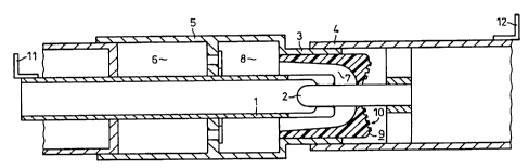
Figure 1 shows a diagrammatic longitudinal section
through an insulating material nozzle for a power switch, in
which the insulating material is PTFE.
Figure 2 shows a top view of the insulating material
nozzle according to the present invention.
Figure 3 shows diagrammatically, in longitudinal section,
a double-nozzle power switch having a compression cylinder
comprising of an insulating material.
DETAILED DESCRIPTION OF THE INVENTION
Figure 1 shows a power switch in its "on" position.
Two arc contact pieces 1 and 2, as well as two continuous-
current contact pieces 3 and 4 lie opposite each other and are
in contact with each other when the switch is turned on.
Electric connections of the switch are designated 11, 12 and
are shown merely diagrammatically.
In order to turn the switch off, the displaceable arc-
contact piece 1 as well as the continuous-current contact
piece 3 which is connected to it using a compression cylinder
5 are moved to the left in Figure 1. This is done by a switch
drive, not shown in detail.
At the same time, arc-extinguishing gas is compressed
within a compression chamber 6.
After the separation of the two arc contact pieces 1 and
2 from each other, an arc is produced between them, with the
arc heating the extinguishing gas within the region of the arc
chamber 7. From arc chamber 7, the hot arc-extinguishing gas
flows into heating chamber 8, where it is temporarily stored
for the subsequent blowing-out of the arc.
After the displaceable arc contact piece 1 has separated
from the stationary arc contact piece 2, the insulating
material nozzle 9, which is made of PTFE, also separates from
SUBSTITUTE SPECIFICATION
CA 02221942 1997-11-21
the stationary arc contact piece 2. The insulating material
nozzle 9 is connected to the compression cylinder 5 in the
region of the continuous-current contact 3.
After the insulating material nozzle 9 has separated from
5 the stationary arc contact piece 2, end face 10 of the
insulating material nozzle is dielectrically stressed by the
electric field between arc contact pieces 1 and 2. In this
region, substantially concentric grooves (Figure 2) of a width
and depth of about 1 mm are produced by machining (for
instance by cutting a spiral groove in the end surface),
whereby a ridge of rectangular cross section having a width of
about 1 mm is produced between the grooves.
An arrangement in accordance with the present invention
is dielectrically safer than a component provided with an
overall better surface quality produced by manufacture.
Figure 3 shows a double-nozzle switch with two fixed
nozzle-shaped contact pieces 13 and 14 which are conductively
connected to each other by a bridging switch piece 15 when the
switch is turned on. A compression device for an arc-
extinguishing gas, consisting of a stationary compression
piston 16 and a movable compression cylinder 17, is provided.
When the switch is turned off, the compression cylinder is
pulled back to such an extent that its bottom 18 is located in
the separation gap between the stationary contact pieces 13,
14 and is exposed there to the electrical field. Bottom 18
has, on its side facing the switch path when it is turned-off,
a structure of saw-tooth shape in cross section, which permits
a discharge of surface charges.
SUBSTITUTE SPECIFICATION