Note: Descriptions are shown in the official language in which they were submitted.
CA 02222109 1997-11-2~
SVG-4020
REDUCTION OF PATTERN NOISE IN SCANNING
LITHOGRAPHIC SYSTEM ILLUMINATORS
Field of the Invention
The present invention relates generally to an illumination
system used in photolithography for the manufacture of
semiconductor devices, and more particularly to an illumination
system using multiplex arrays or multi-image optical elements.
Bac~yL~d of the Invention
In the manufacture of semiconductor devices
photolithographic techniques are used to reproduce the image of a
reticle onto a photosensitive resist covered semiconductor wafer.
The reticle contains patterns that are imaged onto the
photosensitive resist covered wafer. After a series of exposures
and subsequent processing, a semiconductor device containing a
circuit pattern thereon is manufactured. An illumination system
is used to provide a flux of electromagnetic radiation for the
CA 02222109 1997-11-2~
SVG-4020
projection of the image of the reticle onto a semiconductor
wafer. The image of the reticle is formed by an optical
projection system that collects the electromagnetic radiation
after passing through the reticle and projects the image of the
reticle onto the photosensitive resist covered semiconductor
wafer. As semiconductor device manufacturing technology advances,
there are ever increasing demands on each component of the
photolithography system used to manufacture the semiconductor
devices. This includes the illumination system used to illuminate
the reticle. There are many prior illumination systems that
enhance uniformity of illumination and minimize loss of light.
One such illumination system is disclosed in U.S. Patent No.
5,300,971 entitled "Projection Exposure Apparatus" issuing to
Kudo on April 5, 1994, which is herein incorporated by reference.
Therein disclosed is an illumination system having a pulsed light
source with a rotating deflecting prism used to direct the pulsed
light to a fly's eye lens separated from the optical axis. A
condenser is then used to condense the light from the fly's eye
lens for illuminating a reticle. Another illumination system is
disclosed in U.S. Patent No. 5,296,892 entitled "Illuminating
Apparatus and Projection Exposure Apparatus Provided With Such
CA 02222109 1997-11-2~
SVG-4020
Illumination Apparatus" issuing to Mori on March 22, 1994, which
is herein incorporated by reference. Therein disclosed is an
illumination system having an optical integrator or a fly's eye
lens positioned before a condenser. The optical integrator or a
fly's eye lens is designed to be replaceable so that the
numerical aperture on the emission side of the illumination
system can be varied. Another illumination system is disclosed
in U.S. Patent No. 5,245,384 entitled "Illuminating Optical
Apparatus and Exposure Apparatus Having The Same" issuing to Mori
on September 14, 1993, which is herein incorporated by reference.
Therein disclosed is an illumination system having an afocal zoom
optical system placed before an optical integrator or fly's eye
lens to vary the size of a plurality of secondary light sources.
Yet another illumination system is disclosed in U.S. Patent No.
5,237,367 entitled "Illuminating Optical System and Exposure
Apparatus Utilizing The Same" issuing to Kudo on August 17, 1993,
which is herein incorporated by reference. Therein disclosed is
an illumination system having a first optical integrator or fly's
eye lens and a first condenser followed by a second optical
integrator or fly's eye lens and a second condenser. The second
condenser then provides illumination to a reticle. Either the
CA 02222109 1997-11-2~
SVG-4020
first optical integrator or fly's eye lens and the first
condenser have a variable focal length. A further illumination
system is disclosed in US Patent No. 4,939,630 entitled
"Illumination Optical Apparatus" issuing to Kikuchi et al on July
3, 1990, which is herein incorporated by reference. Therein
disclosed is an illumination system having a first optical
integrator or means for forming a plurality of light source
images followed by an optical system containing a second optical
integrator or tertiary light source forming means followed by a
condenser which directs illumination onto a reticle. A further
illumination system is disclosed in US Patent No. 5,534,970
issuing to Nakashima et al on July 9, 1996, which is herein
incorporated by reference. Therein disclosed is an illumination
system that uses a scanning pivot mirror to scan interference
fringes to obtain desired illumination in a scanning exposure
apparatus. Additionally, moving diffusers and other well
established techniques have been used in the past in an effort to
obtain more desirable illumination properties.
While many of these prior illumination systems have provided
improved illumination for their particular application, there is
still a need to provide an illumination system that can be easily
CA 02222109 1997-11-2~
SVG-4020
manufactured and provides uniform illumination and eliminates or
reduces pattern noise effects that may occur in these prior
illumination systems when illumination sources that have
coherence properties, such as a laser, are used in a scanning
lithography system.
Summary of the Invention
The present invention may be used in an illumination system
that uses a multiplex array or multi-image optical element as
part of the illumination system in a scanning lithography system
used to pro]ect a portion of a reticle onto a photosensitive
resist covered wafer. An illumination system according to the
present invention may comprise an illumination source, such as a
pulsed laser, and optical components such as a beam conditioner,
(at least one) multiplex array or multi-image optical element, a
condenser, and a relay. A spatial frequency modulator is coupled
to the (at least one) multiplex array or multi-image optical
element. The spatial frequency modulator effectively moves the
multiplex array or multi-image optical element in a spatial
direction of the direction of scan of the scanning lithography
system. The multiplex array may also have a pattern that is
CA 02222109 1997-11-2~
SVG-4020
spatially frequency modulated in the scanning dimension. The
modulation is sufficient so that a periodic pattern has a linear
magnification modulation dependent on position. In another
embodiment of the invention the pulse rate of a laser is
frequency modulated. The frequency modulation range and rate are
chosen so that several cycles are completed during a single scan.
Accordingly, it is an object of the present invention to
reduce pattern noise effects resulting from the use of multiplex
arrays or multi-image optical elements used in illumination
systems, and in particular illumination systems using pulsed
laser sources.
It is an advantage of the present invention that it may be
used to improve most illumination systems using a multiplex array
or multi-image optical element.
It is a feature of the present invention that a modulator is
coupled to a multiplex array or multi-image optical element.
It is another feature of the present invention that the
multiplex array has a pattern that is spatially frequency
modulated in the scan direction.
It is another feature of the present invention that the
pulse rate of a laser source is frequency modulated.
CA 02222109 1997-11-2~
SVG-4020
These and other objects, advantages, and features will
become apparent in view of the following more detailed
description.
Brief Description of the Drawings
Fig. 1 schematically illustrates one embodiment of the
present invention.
Fig. 2 schematically illustrates another embodiment of the
present invention.
Fig. 3 is a perspective view of a reticle illustrating the
illumination slot or field.
Fig. 4 is a graph illustrating the intensity profile along
the width of the illumination slot or filed.
Fig. 5 is a graph illustrating an enlarged view of a portion
of the intensity profile illustrated in Fig. 4.
Fig. 6 is a power spectrum graph illustrating regular
patterns and random noise.
Fig. 7 is a graph illustrating a first laser pulse pattern
and a second laser pulse pattern.
Fig. 8 schematically illustrates a multiplex array with a
spatially frequency modulated pattern.
CA 02222109 1997-11-2~
SVG-4020
Fig. 9 is a graph illustrating a pattern with unequal
distances.
Fig. 10 schematically illustrates a multiplex array with
another form of spatially frequency modulated pattern.
Detailed Description of the Preferred Embodiments
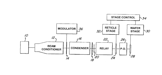
Fig. 1 illustrates one embodiment of the present invention.
An illumination source 10 directs electromagnetic radiation into
a beam conditioner 12. The term illumination source is used in
its broadest sense to mean any electromagnetic radiation source
regardless of wavelength. Therefore, the illumination source 10
may be a laser having a wavelength that is not in the visible
region. Additionally, the illumination source may be a pulsed
laser or a continuous wave laser. The beam conditioner 12
enlarges or modifies the beam of electromagnetic radiation from
the illumination source 10. This may be accomplished by a beam
expander such as a refractive optical system, or a reflective
optical system. The conditioned electromagnetic radiation is
directed through a multiplex array or multi-image optical element
14. The multiplex array or multi-image optical element 14 may be
a microlens array comprised of a plurality of refractive lens
CA 02222l09 l997-ll-2~
SVG-4020
elements or a diffractive optical element. Multi-image optical
element 14 directs light to a condenser 16. For a scanning
photolithography system, the condenser 16 iS preferably an
anamorphic condenser in that a rectangular slit illumination
field is formed thereby. The condenser 16 collects light from the
multi-image optical element 14 and directs it to an array optical
element 18. The array optical element 18 may not be used in some
illumination systems. However, the use of the array optical
element 18 may be desirable in some applications as indicated in
US Patent application 08/449,301 filed May 24, 1995 and entitled
"Hybrid Illumination System for Use in Photolithogrphy", which is
herein incorporated by reference. An illumination plane 20 is
formed after the condenser 16 and optional array optical element
18. Relay 22 iS used simply to conjugate the illumination plane
20 to a reticle 24. The image of the reticle 24 iS projected by
projection optics 26 onto the wafer 28. Reticle 24 iS placed on
and moved by a reticle stage 32. The wafer is placed on and moved
by a wafer stage 30. Stage control 34 controls the movement of
reticle stage 24 and wafer stage 30. The movement of the reticle
stage 24 and the wafer stage 30 are generally synchronized in
proportion to the magnification of the system. A modulator 36 iS
-
CA 02222109 1997-11-2~
SVG-4020
coupled to multiplex array or multi-image optical element 14.
The modulator 36 spatially frequency modulates the multiplex
array or multi-image optical element in the scanning dimension so
that a periodic pattern has a linear magnification dependent on
position. When this pattern is multiplicatively printed in the
scanning process the patterns can be made so aliasing will not
occur. It should be appreciated that the present invention is not
limited to the illustrated illumination system described, but is
applicable to any illumination system utilizing a multiplexing
array or multi-image optical element whether for controlling
macro uniformity, the numerical aperture of the illumination
system, or partial coherence of the lithographic system. This
system decoheres any residual pattern (or regular variance in
illumination) by having multiple spatially displaced illumination
"patches", by small amounts, such that over the plurality of time
for exposure many displaced fields are overlaid and regular
pattern noise will be averaged.
Fig. 2 illustrates another embodiment of the present
invention. In Fig. 2 a pulsed laser source 110 provides
electromagnetic radiation to beam conditioner 12, and then to a
multiplex array or multi-image optical element 14, then to a
-
CA 02222l09 l997-ll-2~
SVG-4020
condenser 16, and a array optical element 18, forming an
illumination plane 20. The illumination plane 20 iS conjugated by
relay 22, to illuminate a reticle 24. The image of the reticle 24
is projected by projection optics 26 onto a photosensitive resist
covered wafer 28. The position of the reticle 24 and the wafer 30
is controlled by reticle stage 32, wafer stage 20 and stage
control 34. The embodiment illustrated in Fig. 2 iS similar to
the embodiment illustrated in Fig. 1, however a frequency
modulator 136 iS coupled to pulsed laser source 110. The
frequency modulator 136 modulates the pulse rate of the pulse
laser 110. The frequency modulation range and the frequency
modulation rate are chosen so that several cycles of the
frequency modulation range can be completed or done during the
scan time or in a single scan. This will ensure that no aliasing
will occur. Each pulse will have associated with it a periodic
spatial modulation. If the pulse rate changes over an exposure
time then these patterns will not overlap in space and averaging
will occur. That is, as the pulse rate changes the patterns will
move with respect to the exposed wafer as it scans and have a
different position preventing any overlap and therefore any
cumulative effect that can degrade imaging.
CA 02222109 1997-11-2~
SVG-4020
Fig. 3 more clearly illustrates the scanning illumination
slot or field formed with the present invention. A reticle frame
38 holds a reticle 24. A rectangular illumination slot or field
40 is formed that has a width w. The illumination slot or field
40 is scanned in a longitudinal direction across the reticle 24
in the x direction indicated by the arrow 41. Typically, the
reticle frame 38 is attached to a reticle stage, not illustrated,
moving the reticle 24 relative to the illumination slot or field
40.
Fig. 4 graphically illustrates the illumination intensity
profile across the width of the illumination slot or field. Wave
form 42 represents the illumination intensity in the width or x
direction. While the illumination intensity appears relatively
uniform, as desired, often there is micro non-uniformity.
Fig 5 is an enlarged section of a portion of the wave form
42 illustrated in Fig. 4 showing the micro non-uniformity of the
illumination intensity. Wave form 44 illustrates characteristic
spatial non-uniformity from a lower limit set by the spatial
frequency pass band of the projection optics used. Higher spatial
frequencies may be present, but are generally not of interest.
Typically, 0.2 ~m for a high numerical aperture, 0.60, system
CA 02222109 1997-11-2~
SVG-4020
with magnification scaling as needed. This micro non-uniformity
is not desirable as it will often result in imaging problems,
such as lack of linewidth control, linewidth variation, edge
roughness, and other phenomena known to those skilled in the art.
Fig. 6 graphically illustrates the intensity as a function
of frequency of the micro non-uniformity illustrated in Fig. 5.
Peak wave form portions 46 represent a fixed or periodic
component and wave form portions 48 represent a random pattern.
This is in reference to a pulsed laser source, but applies to a
continuous source with some limitations. Point 50 is the system
band pass upper limit. In a scanning lithography system the
random component illustrated by wave form portion 48 will be
averaged out with a reduction in the noise or illumination micro
non-uniformity variation of the square root of the number of
pulses employed per unit exposure position. The periodic complex
component may or may not be reduced in magnitude depending on the
aliasing between the scan velocity, pulse rate, and pattern
frequency.
Fig. 7 graphically illustrates a first pulse pattern
represented by wave form 52 and a second pulse pattern
represented by wave form 54. In Fig. 7 a phase aliasing condition
CA 02222109 1997-11-2~
SVG-4020
is illustrated which is detrimental. The occurrence of these
aliasing portions will be complex, therefore a look up table to
prevent operation of the scanning stage at predetermined velocity
components is inconvenient and not reliable. The present
invention ensures absence of aliasing with consequent higher
reliability of the lithography system. Since any one small
portion in the scanned field may receive an exposure from
multiple pulses, these periodic complex components may overlap
and not average out. This will compromise the quality of the
exposure and the image.
Fig. 8 schematically illustrates a multiplex array that has
a spatially frequency modulated pattern that may be used at the
locations of multiplex arrays 14 and/or 18 illustrated in Fig. 1
and 2. However, it should be appreciated that when the multiplex
array illustrated in Fig. 8 is used at the locations of multiplex
arrays 14 and/or 18, the modulator 36 illustrated in Fig. 1 and
the frequency modulator illustrated in Fig. 2 would usually not
be needed. The regular patterns or components 46 illustrated in
Fig. 6 are generally the result of the periodic structure of a
multiplexing array. By providing a spatially frequency modulated
pattern of elements on the multiplexing array, of the present
-
CA 02222l09 l997-ll-2S
SVG-4020
invention, any resulting pattern has a linear magnification
dependent on position. That is, the distances in the scan
direction between wave forms of the resulting pattern will not be
equal. Fig. 9 graphically represents the unequal distances
between adjacent wave forms in the resulting pattern. When this
pattern is mutiplicatively printed in the scanning process the
patterns may be made so that aliasing will not occur. As
illustrated in Fig. 8, the multiplex array has elements in four
different sections, 60, 62, 64, and 66. Each section 60, 62, 64,
and 66 iS comprised of elements different than the adjacent
sections. For example, section 60 may be comprised of elements
having a dimension of 100 units, section 62 may be comprised of
elements having a dimension of 110 units, section 64 may be
comprised of elements having a dimension of 120 units, and
section 66 may be comprised of elements having a dimension of 130
units. The units are provided only to indicate relative size and
may be any typical unit dimension for a multiplex array.
Accordingly, the multiplex array has a spatially frequency
modulated pattern. This spatially frequency modulated pattern
need only be modulated in the direction of scan. Arrow 76
represents the direction of scan. Additionally, the spatially
-
CA 02222109 1997-11-2~
SVG-4020
frequency modulated pattern illustrated in Fig. 8 as sections 60,
62, 64, and 66 are intended only to schematically represent a
multiplex array. The elements 68, 70, 72, and 74 are
schematically illustrated as different circle sizes, but may be
any shape or pattern commonly used for an element in a multiplex
array. The elements 68, 70, 72, and 74 extend along the entire
longitudinal length of each respective section 60, 62, 64, and
66. Additionally, while only four sections 60, 62, 64, and 66 are
illustrated in Fig. 8, there may be any number of sections. The
sections may also repeat, that is a group of sections may be
repeated forming multiple cycles in a single multiplex array.
Fig. 10 illustrates this form of spatially frequency modulating
the multiplex array. In Fig. 10 the multiplex array is formed
from repeating longitudinal sections 80, 82, and 90. Each of the
sections 80, 82, and 90 comprises an element 86, 88, and 90,
respectfully, having a different dimension. Longitudinal sections
80, 82, and 90 form one cycle of the pattern which is repeated in
the direction of scan. Therefore, three cycles are illustrated.
The scanning direction is preferably substantially perpendicular
to the longitudinal dimension of the sections 80, 82, and 90.
CA 02222109 1997-11-2~
SVG-4020
Accordingly, the present invention helps to eliminate
pattern noise effects in illumination systems using multiplex
arrays or multi-image arrays. As a result the present invention
provides better illumination for use in a scanning lithography
system increasing linewidth control, edge roughness, and other
imaging properties.
Additionally, although the present invention has been
illustrated with reference to a particular illumination system it
should be appreciated that the present invention may be applied
to other illuminations systems with a multiplex array or multi-
image array. Therefore, it will be obvious to those skilled in
the arts that various modifications may be made without departing
from the spirit and scope of this invention.