Note: Descriptions are shown in the official language in which they were submitted.
CA 02222462 2001-02-02
66446-657
1
METHOD AND APPARATUS FOR A UNIQUE WORD DIFFERENTIAL DETECTION
AND DEMODULATION USING THE UNIQUE WORD DIFFERENTIAL DETECTION
Background of the Invention
The present invention relates to a unique word
differential detection method and a demodulator using the
unique word differential detection which detect a known unique
word (UW) and a carrier frequency offset of a quasi-
synchronized detection signal by using a differential detecticn
technique or the quasi-synchronised detection signal which
quasi-synchronously detects an orthogonal modulation signal in
which the known unique word is inserted in a data signal.
Such a unique word differential detection system has
a feature that, when the orthogonal modulation signal is quasi-
synchronously detected by using a local. oscillator signal
independent from the orthogonal modulation signal, the unique
word can be detected even. if there is a frequency difference
between the carrier of the orthogonal modulation signal and the
local oscillator signal, that is, even if there is a carrier
frequency offset. In addition, it also has a feature that the
unique word can be detected at a high speed. A unique word
detector disclosed in Japanese Patent Application Laid-Open No.
5-167630 is one of such unique word differential detection
systems. Now, a conventional unique word differential
detection system is described with reference to Figs. 1, 2 and
3.
Fig. 1 is a format of data signal according tc the
present invention. Fig. 2 is a functional block diagram
showing a unique word differential detection system according
to the related art. The unique word differential detection
circuit shown in the figure is a basic circuit for the unique
word differential detection system according to the present
invention. In addition, Fig. 3 is a diagram for illustrating
CA 02222462 2001-02-02
66446-657
2
the operation of the unique word differential detection system
of Fig. 2.
Referring to Fig. 1, a base-band data signal
according to the present invention constitutes one frame with a
unique word (hereinafter sometimes abbreviated to UW) having a
known L symbol train and data of a plurality of symbols. The
UW is used for a frame signal. The data signal typically has a
UW of 30-50 symbols, data of 200-400 symbols, and one frame
interval Tf of 40-200 milliseconds (mS). The UW is positioned
at the top of each frame. A symbol repetition frequency is
represented by Fs (symbol/S), and one symbol interval is
represented by Ts=1/Fs (S).
Referring to Fig. 2, a UW differential detector
circuit 100 is supplied with a received quasi-synchronized
detection signal S100=R (t) and a local. unique word Suw=U (t)
obtained by generating a known UW. Then, it outputs a mutually
correlated signal S 107=D (t) which is a signal which
differentially detects th.e signal 5100 mutually correlated with
a signal which differentially detects the unique word Suw. The
quasi-synchronized detection signal 5100 is a signal which
quasi-synchronously detects the orthogonal modulation signal
with the known UW inserted in the data signal. The quasi-
synchronized detection means synchronously detects the
orthogonal modulation signal with a local oscillation signal
independent from the orthogonal modulation signal but with a
frequency close to that of the orthogonal modulation signal and
to demodulate the orthogonal modulation signal into the data
signal at base ban. Generally, there is a frequency difference
Fo (Hz/S) or a carrier frequency offset (hereinafter called the
"frequency offset") Fo between the carrier of the orthogonal
modulation signal and tr.e local oscillation signal.
CA 02222462 2001-02-02
66446-657
3
The quasi-synchronized detection signal 5100 consists
of two trains of in-pha;~e (I) signals and quadrature (Q)
signals. In the follow:i:ng, by considering that the quasi-
synchronized detection signal S100 is a complex signal of I and
~~ Q signals, the in-phase component of a signal R (t) may be
referred to as ReR (t) meaning a real signal. component, and the
quadrature signal component may be referred to as ImR (t)
meaning an imaginary si~~nal component. The signal R (t) is a
signal with an inverted code "1" or "-1". ReR (t) and ImR (t)
of the quasi-synchronized detection signal 5100 are inserted
with the same UW in the same timing, respectively. The quasi-
synchronized detection signal R (t) is expressed by Formula (1)
if there is the frequency offset FO.
R (t) - S (t) . e72n(FO.t+ga> . . . . . (1)
1~> where S (t) is data to be transmitted, and assumed to be QPSK
modulated.
S (t) _ e~a,rck(v=)/4) . . . . . (2)
where k (t) is the number of modulation phase of the orthogonal
modulation signal. at time t, and 8a is any phase. When it is
assumed that an L symbol interval of the UW is
T (0 < T < L ~ Ts = L/F's), and n is a frame number, a unique
word U (t) is expressed by Formula 3) in a unique word interval
T.
U (T) - S (n ~ Tf + T) . . . . . (3)
2!~ The UW differential detector circuit 100 delays the
quasi-synchronized detection signal 5100 - R (t) with the delay
circuit lOla by N symbols (= N ~ Ts seconds) (N is any positive
number), and the N symbol delayed signal 5101 is complex
conjugated by a complex. conjugate circuit 102a. That is, the
CA 02222462 2001-02-02
66446-657
4
complex conjugate circuit 102a inverts the code of ImR (t) of
the N symbol delayed R (t), and N symbol delays and complex
conjugates the quasi-synchronized detection signal R (t) to
generate a complex conjugate signal S102. A multiplier 103a
multiplies the quasi-synchronized detection signal 5100 with
the complex conjugate signal 5102, that is, N symbol complex
conjugates, delays and detects the quasi-synchronized detection
signal 5100 to generate a data signal differential detection
signal 5103. The data signal differential detection signal
1C S103 in a T interval is expressed by Formula (4), where R* is
the
CA 02222462 1997-11-26
- 5 -
complex conjugate of the quasi-synchronized detection signal
R (t).
5103 = R (n ~ Tf + z) ~ R* (n ~ Tf + t - N ~ Ts) ... (4)
On the other hand, a unique word Suw = U (t} of the
base band repeating the same signal train as the unique word
in the guasi-synchronized detection signal 5100 is input
into the delay circuit lOlb and the complex conjugate
circuit 102b. The unique word Suw may insert a signal in
the same format as the quasi-synchronized detection signal
5100 therebetween. The unique word U (t) also consists of
two trains, a real signal component ReU (t) and an imaginary
signal component ImR (t). The delay circuit lOlb generates
an N symbol delayed signal 5104 which is the unique word Suw
- U (t) delayed by N symbols. The complex conjugate circuit
102b complex conjugates the unique word U (t), that is,
inverts the code of ImU (t) to generate a complex conjugate
signal Si05. A multiplier 103b multiplies the N symbol
delay signal 5104 with the complex conjugate signal 5105, N
symbol complex conjugates, delays and detects the unique
word Suw to generate a UW differential detection signal
5106. The UW differential detection signal 5105 is
expressed by Formula (5), where U* is complex conjugate of
the unique word U (t). The resultant UW differential
detection signal 5106 is sent to a correlator 104, and
stored as a reference for correlation detection.
S106 (z) - U (T - N ~ Ts) ~ U* (z) ... (5)
The correlator 104 cross correlates the data signal
differential detection signal 5103 being sequentially sent
8 d 99E960I09E/89~bI/I0~9I (Y) BS~~iI1~L661 03IV 'tdOISIAIQ 'd 'I Y~IO~I3
CA 02222462 2001-02-02
66446-657
6
and the stored UW differential detection signal 5106 over L
symbols, or over the ent~:ire symbol length of the UW. If N=1,
the correlator 104 generates a cross correlation signal
5107 = D (t) as understood by Formula (6).
5107 (t) - D(n~Tf + t)
- fOL/Fs X5103 (t -~ T) ~ slo6 (T) ~ dT
-~OL/FS ~S(mTf. + t + T) ~S*(mTf + t + T - Ts) . . . (6)
ej2n[F (n~Tf+t+Tji-i3a] , e-j2n(FO(n~Tf+t+T-Ts) + Aa]
0
U (T-Ts ) ~ U* (T) ] dT
1C If t = 0 where timing of the unique word in the
quasi-synchronized detection signal R (t) matches timing of the
unique word U (t), Formula (6) can be expressed by Formula (7).
5107 (t=0) _ (L/hS) .ej2nFOTs . . . . . (7)
In Formula (7), the cross correctional signal
1G~ 5107 = D (t) has an amplitude of (L/Fs) and a value of phase
angle 8 of (2TrF0~Ts). That is, a phase term 8 is proportional
to a product of the frequency offset Fo and the delay time
(N x Ts). Alternative ly, the frequency offset Fo is expressed
as Fo = e/ (2TTTs) - e~Fsj?TT.
20 The correlato:r 104 divides the cross correlation
signal 5107 = signal D (t) into a real component Re and an
imaginary component Im, and outputs them. That is, the cross
correlation signal 5107 has a relationship of
(L/Fs) - (Rez + Imz) 1/z for amplitude, and a relationship of
2ci Re = (L/Fs)~cos e, Im = (L/Fs) ~ sin B for the phase term B.
A UW detector 105 squares the Re and Im of the cross
correlation signal S107, respectively, to generate a power
CA 02222462 2001-02-02
66446-657
7
value (L/Fs)2. If timing of the unique word in the quasi-
synchronized detection signal R (t) matches timing of the
unique word U (t), the power value (L/Fs)2 produces a peak at
the position of the last symbol of the unique word Suw. The UW
detector 105 compares the power value (L/Fs)2 and a
predetermined threshold Sth. The threshold Sth is determined
by taking into consideration the magnitude of the reception
error of the quasi-synchronized detection signal R (t) or the
like. If the power value (L/Fs)z is larger than the threshold
Sth, the UW detector 105 produces a UW detection signal 5108
indicating that a UW is detected from the quasi-synchronized
detection signal 5100. The UW detection signal 5108 is used as
a frame synchronization signal in synchronization demodulation
of the quasi-synchroni~~ed. detection signal 5100, or the like.
A UW phase arithmetic unit 106 calculates a phase
term 8 from the Re and Im contained in the cross correlation
signal 5107 to generate frequency offset information 5109.
Here, since the UW phase arithmetic unit 106 calculates the
phase term 8 of a cross correlation function D (t) as tan-1
(Im/Re), the determinable upper limit of phase term 8 is ~n.
Therefore, the measurement range of the frequency offset FO
becomes ~Fs/2 or less for Ts = 1 (N = 1) symbol time.
Fig. 3 shows a measurement range of the frequency
offset Fo for N symbols, amount of delay for the quasi-
synchronized detection signal R (t) and the unique word U (t)
in the UW differential detector circuit 100. That is, the
measurement range of the frequency offset Fo is inversely
proportional to the number of delay symbols N. On the other
hand, resolution of the frequency offset Fo (frequency
resolution) would be proportional to the amount of delay N.
The frequency offset information 5109 is used as correction
information for carrier frequency offset in the synchronous
CA 02222462 2001-02-02
66446-657
8
demodulation of the quasi-synchronized detection signal 5100,
or the like.
The above-mentioned conventional unique word
differential detection system has features not only being
capable of detecting a unique word even if there is a carrier
frequency offset, but also being fast in detecting the unique
word.
However, the conventional unique word differential
detection system has the first problem that, as shown in Fig.
3, the measurement range of carrier frequency offset is in a
relationship of tradeoff with the resolution, so that both
cannot be simultaneously enhanced.
The second problem lies in that the unique word
differential detection system does not have a measure for
protecting false detection of the unique word.
In addition, the third problem lies in that, when the
carrier frequency offset has a high magnitude, the unique word
differential detection system cannot prevent a unique word
detection capability from being deteriorated due to noise and
adjacent channel interference (ACI), and noise containing ACI
from being increased in a signal supplied to a demodulator.
Furthermore, the fourth problem lies in that in
estimating timing of the unique word by the unique word
differential detection system, signal processing speed is
reduced when estimation accuracy is increased.
Summarv of the Invention
The present invention is intended to provide a unique
word differential detection system which can solve the first to
fourth problems in the prior art.
CA 02222462 2001-02-02
66446-657
9
The unique word differential detection system
according to the present invention mainly solves the first and
fourth problems in the prior art, detects the position of the
UW with a high accuracy, and expands a measurement range for
frequency offset of the quasi-synchronized detection signal
while maintaining the measurement accuracy at a high level. To
this end, it maintains the operating state of an initial
acquisition mode (hereinafter abbreviated as an IA mode) which
comprises a plurality of UW differential detector delay
circuits each having different number of delay symbols, the UW
differential detector delay circuit being based on the UW
differential detector circuit 100. An IA mode UW differential
detector delay circuit used in the IA mode comprises a UW
differential detector delay circuit with the number of delay
symbols N (where 0.5 < N <_ 1)
CA 02222462 1997-11-26
_ 10
(hereinafter abbreviated as DDD {N)), and a UW differential
detector delay circuit with N' - N/2 (hereinafter
abbreviated as DDD (N/2)). An IA mode UW detector circuit
responds to cross correlation signals output from the DDD
{N) and DDD (N/2), respectively, and generates an IA mode UW
detection signal indicating detection of unique word from a
first supplied quasi-synchronized detection signal, and an
IA mode frequency offset information indicating the
frequency offset Fo of the first quasi--synchronized detection
signal.
The unique word differential detection system according
to the present invention mainly solves the second and third
problems in the prior art, and performs a fine tune
acquisition mode (hereinafter abbreviated as the FA mode)
after detection of the UW in the IA mode. For the FA mode,
it comprises an FA mode UW differential detection delay
circuit with the number of delay symbols M (where, 1 < M)
(hereinafter abbreviated as the DDD {M)). An FA mode UW
detector circuit responds to a cross correlation signal
output from the DDD (M), and generates at least an FA mode
UW detection signal indicating detection of a unique word
from a second quasi-synchronized detection signal
corresponding to the first quasi-synchronized detection
signal.
To apply the unique word differential detection system
to a decoder, when the FA mode UW detection signal occurs,
the present invention terminates the UW detection operation
and turns to a steady state mode (hereinafter abbreviated as
6l d 99E960I 098/89 ~ b Is/EO ~ 9I (Y) 89~~~l 1~~66I O~t~i 'IUOIS IAIQ 'd -I
hiO~I3
CA 02222462 2001-02-02
66446-657
11
the SS mode) to demodu_Late the data signal by synchronously
detecting the second quasi--synchronized detection signal. The
above-mentioned unique word differential detection system and
the demodulator according t=o the present invention are
frequently constituted by a digital. signal processor (DSP in
the following) in which a microprocessor and a storage circuit
are controlled by software.
In accordance with the present invention, there is
provided a unique word differential detector comprising: a
first differential detE=ction delay (DDD) for cross correlating
an input signal inserted with a unique word (UW) and said UW
previously input after differentially detecting each of them
with a delay symbol of N (0.5 < N ~ 1); a second DDD for cross
correlating said input signal and said UW after differentially
detecting each of them with a delay symbol of N/2; and first UW
detector means for detecting a first UW detection signal and a
first frequency offset of said input signal based on an output
of said first and second DDD.
In accordance with the present invention, there is
provided a demodulator using a unique word differential
detector comprising: first UW detector means for detecting a
first UW detection signal and frequency offset of an input
signal by using a fist differential detection delay (DDD) for
cross correlating said input signal inserted with a unique word
(UW) and said UW previously input after differentially
detecting each of them with a delay symbol of N (0.5 < N ~ 1),
and a second I~DD for cross correlating said input signal and
said UW after different=ially detecting each of them with a
delay symbol of N/2; second UW detector means for outputting a
second UW detection signal using a third DDD, said third DDD
cross correlai~ing an input signal compensated for offset
frequency based on said frequency offset and said UW after
CA 02222462 2001-02-02
66446-657
12
differentially detectlIlg each of them with a delay symbol of M
(1 < M); and demodulator means for demodulating said input
signal through synchronized detection after said second UW
detection signal is detected by said second UW detector means.
In accordance with the present invention there is
further provided a method of a unique word differential
detector, said method comprising the steps of: when the
detector is in an init_i.al acquisition mode (IA mode), cross
correlating an input s=Lgnal inserted with a unique word (UW)
and said UW previously input after differentially detecting
each of them with a delay :symbol of N ( 0 . 5 < N ~ 1 ) by a f first
differential detection delay (DDD); cross correlating said
input signal and said tJW af=ter differentially detecting each of
them with a delay symbol of. N/2 by a second DDD; detecting a
first UW detection signal and frequency offset of an input
signal based on output~~ of said first and second DDD; and when
the detector is in a f_i.ne tune acquisition mode (FA mode),
outputting a second UW detection signal using a third DD:D, said
third DDD cross correlating an input signal compensated for
offset frequency based on said frequency offset and said UW
after differentially detecting each of them with a delay symbol
of M ( 1 < M) .
In accordance with the present invention there is
further provided a method of demodulation using a demodulator
having a unique word differential detector, said method
comprising the steps oi=: when the detector is in an initial
acquisition mode (IA mode); cross correlating an input signal
inserted with a unique word (UW) and said UW previously input
after differentially detecting each of them with a delay symbol
of N (0.5 < N ~ 1) by a first differential detection delay
(DDD); cross correlatiTlg said input signal and said UW after
differentially detectlTlg each of them with a delay symbol of
CA 02222462 2001-02-02
66446-657
13
N/2 by a second DDD; df~tect~ing a first UW detection signal and
frequency offset of an input signal based on outputs of said
first and second DDD; when the detector is in a fine tune
acquisition mode (FA mode); outputting a second UW detection
signal using a third DDD, raid third DDD cross correlating an
input signal compensated for offset frequency based on said
first frequency offset and said UW after differentially
detecting each of them with a delay symbol of M (1 < M); and
moving to a steady stage mode (SS mode) after outputting said
second UW detection signal in said third DDD step, wherein said
input signal :LS demodulated through synchronized detection.
In accordance with the present invention, there is
further provided a unique word differential detector
comprising: first frequency shifter means for shifting an input
signal inserted with a unique word (UW) by a first frequency; a
first differential detection delay (DDD) for cross correlating
an input sign<~l shifted by said first frequency and said UW
previously input after differentially detecting each of them
with a delay symbol of N (0.5 < N ~ 1); a second DDD for cross
correlating an input signal shifted by said first frequency and
said UW after differeni~ially detecting each of them with a
delay symbol of N/2; first UW detector means for detecting a
first UW detection signal, and first and second phase
information based on the outputs of said first and second DDD;
second frequency shifts=_r means for shifting the input signal by
a second frequency to define a second shifted input signal; a
third DDD for cross correlating the second shifted input signal
with the UW after different=ially detecting each of them with a
delay symbol of N (0.5 < N ~ 1); a fourth DDD for cross
correlating the second shifted input signal with the UW after
differentially detecting each of them with a delay symbol of
N/2; second UW detecto:r_ me<~ns for detecting a second UW
detection signal, and ~h.ird and fourth phase information based
CA 02222462 2001-02-02
66446-657
14
on outputs of said third and fourth DDD; first selector means
for selecting a larger one of the first and second UW detection
signals; second selector means for selecting one of a first
phase synthesized valu~= synthesizing said first and second
phase information and a second phase synthesized value
synthesizing said third and fourth phase information in the
same side as selected by said first selector means; and third
UW detector means for detecting a third UW detection signal
based on an ovatput of ~sa.i.d first selector means, and detecting
a frequency offset of 'the :input signal based on an output of
said second selector m~~a.ns.
In accordance with the present invention there is
further provided a demodulator using a unique word differential
detector comprising: first frequency shifter means for shifting
an input signal inserted with a unique word (UW) by a first
frequency; a first differential detection delay (DDD) for cross
correlating an input signal shifted by the first frequency and
the UW previously input after differentially detecting each of
them with a delay symbol o:E N (0.5 < N ~ 1) ; a second DDD for
cross correlating an input signal shifted by said first
frequency and the UW after differentially detecting each. of
them with a delay symbol of N/2; first UW detector means for
detecting a first UW detection signal, and first and second
phase information based on outputs of said first and second
DDD; second frequency shifter means for shifting the input
signal by a second frequency; a th_Lrd DDD for cross correlating
an input signal shifted by said second frequency and the UW
previously input after di.f:ferentially detecting each of them
with a delay symbol of N (0.5 < N ~ 1) ; a fourth DDD for cross
correlating an input signal shifted by the second frequency and
the UW after differentially detecting each of them with a delay
symbol of N/2; second UW detector rneans for detecting a second
UW detection signal, and third and fourth phase information
CA 02222462 2001-02-02
66446-657
based on outputs of said third and fourth DDD; first selector
means for selecting a larger one of the first and second UW
detection signals; second aelector means for selecting one of a
first phase synthesized value synthesizing said first and
5 second phase information and a second phase synthesized value
synthesizing said third and fourth phase information wherein
said second selector means selects a phase synthesized value
corresponding to a UW detection signal selected by said first
selector means; third UW detector means for detecting a third
10 UW detection signal based on an output of said first selector
means, and detecting a frequency offset of the input signal
based on said second selector means; a third DDD for cross
correlating a frequency compensated input signal with th.e UW
after differentially detecting each of them with a delay symbol
15 of M (1 < M); third UW selector means for outputting a third UW
detection signal by using said third DDD; and demodulator means
for demodulating the input signal through synchronized
detection after the third ~JW detection signal is detected by
said third UW detector means.
In accordance with the present invention, there is
further provided a method of detection using a unique word
differential detector, said method comprising the steps of:
when the detector is iw an initial acquisition mode (IA mode),
shifting an input signal inserted with a unique word (UW) by a
first frequency; cross correlating an input signal shifted by
said first frequency and said UW previously input after
differentially detecting each of them with a delay symbol of N
(0.5 < N ~ 1; by a first differential detection delay (DDD);
cross correlating an input signal shifted by said first
frequency and said UW after differentially detecting each of
them with a delay symbol. of N/2 by using a second DDD;
detecting a first UW detection signal, and first and second
phase information based on the outputs of said first and second
CA 02222462 2001-02-02
66446-657
16
DDD; shifting the input signal by a second frequency to define
a second shifted input signal; cross correlating the second
shifted input signal with the UW previously input after
differentially detecting e<~ch of them with a delay symbol of N
(0.5 < N ~ 1) by using a third DDD; cross correlating the
second shifted input signal and the UW after differentially
detecting each of them with a delay symbol of N/2 by using a
fourth DDD; detecting a second UW detection signal, and third
and fourth phase information based on the outputs of said third
and fourth DDD; selecting a larger one of the first and second
UW detection signals; ;selecting one of a first phase
synthesized value synt~zesizing said first and second phase
information and a second. phase synthesized value synthesizing
said third and fourth phase information in the same side as
selected by said first selector means by second selector means;
detecting a t~~ird UW detection signal based on the output of
said first selector means, and detecting a frequency offset of
the input signal based on said second selector means; and when
the detector is in a fine rune acquisition mode (FA mode);
outputting a third UW detection signal by using the fifth DDD
for cross correlating an. input signal compensated for offset
frequency based on said fi=rst frequency offset and said UW
after differentially d~=_tecting each of them with a delay symbol
of M ( 1 < M) .
In accordance with the present invention, there is
further provided a met~zod of demodulation using a demodulator
having a unique word differential detector, said method
comprising the steps of: when the detector is in an initial
acquisition mode (IA mode), shifting an input signal inserted
with a unique word (UW) by a first frequency; cross correlating
an input signal shifted by said first frequency and said. UW
previously input after differentially detecting each of them
with a delay symbol of 1\f (0.5 < N ~ 1) by a first differential
CA 02222462 2001-02-02
66446-657
17
detection delay (DDD); cross correlating an input signal
shifted by said first frequency and said UW after
differentially detecting each of them with a delay symbol of
N/2 by using a second .DDD; detecting a first UW detection
signal, and first and second phase information based on the
outputs of said first and second DDD; shifting the input signal
by a second frequency; cross correlating an input signal
shifted by said second frequency and said UW previously input
after differentially detecting each of them with a delay symbol
of N (0.5 < N ~ 1) by a third DDD; cross correlating an input
signal shifted by said second frequency and said UW by delaying
each of them by a delay symbol of N/2 by using a fourth DDD;
detecting a second UW de:tection signal, and third and fourth
phase information based on the outputs of said third and fourth
DDD; selecting a larger one of the first and second UW
detection signals; sel,?ct.ing one of a first phase synthesized
value synthesizing said first and second phase information and
a second phase synthesized value synthesizing said third and
fourth phase information. wherein a phase synthesized value
corresponding to a sel~=cted UW detection signal is selected;
detecting a third UW detection signal based on the selection of
the larger one of the first and second UW detection signals,
and detecting a frequency offset of the input signal based on
the phase synthesized value selected; when the detector is in a
fine tune acquisition mode (FA mode), outputting a third. UW
detection signal by using a fifth DDD for cross correlating a
frequency compensated input signal with the UW after
differentially detecting e<~ch of them with a delay symbol of M,
wherein M > 1, and wherein the frequency compensated input
signal is compensated :based on a frequency offset; and moving
to a steady state mode (SS mode) after said outputting step,
wherein the input signal is demodulated through synchronized
detection.
CA 02222462 2001-02-02
66446-657
18
Brief Description of the Drawinqs
Fig. 1 is a data format of data signal containing a
unique word and data;
Fig. 2 is a block diagram showing a conventional
unique word differentia7_ detection system;
Fig. 3 is a relationship between amount of de7_ay, N
symbols, in the convent_~onal unique word differential detection
system and a measurement range for frequency offset Fo.
Fig. 4 is a block diagram showing a first embodiment
of the unique word differential detection system according to
the present invention;
Fig. 5 is a block diagram of NCO 11 in Fig. 4;:
Fig. 6 is a block diagram showing a demodulator using
the unique ward differential detection system of Fig. 4;
Fig. 7 is a block diagram showing a second embodiment
of the unique word differential detection system according to
the present invention;
Fig. 8 is a block diagram showing a demodulator using
2C the unique word differential detection system of Fig. 7,; and
Fig. 9 is a relationship of carrier offset frE=_quency
and spectrum intensity.
Descrit~ticn of the Preferred Embodiments
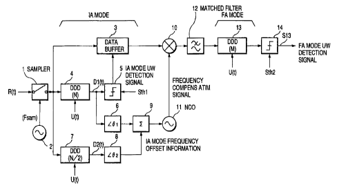
Fic~. 4 is a b:Lock diagram showing a first embodiment
2~~ of the unique word'differential detection system according to
the present invention. A sampling signal generator 2, which
generates a sample rate Fsam of N/symbol or more, samples a
CA 02222462 2001-02-02
66446-657
19
first quasi-synchronized detected orthogonal modulation signal
with a known UW insert.ed in a data signal. The unique word U
(t) is also supplied t.o a DDD (N) 4 and a DDD (N/2) 7. Its
output is supplied to a DDD (N) 4 and a DDD (N/2) 7. The DDD
(N) 4 cross correlates an N symbol complex conjugate
differential detection signal of the sampled first quas:L-
synchronized detection signal with an N symbol complex
conjugate differential detection signal of the UW to generate a
first cross correlation signal Dl (t). The DDD (N/2) 7 cross
correlates an N/2 symbol complex conjugate differential
detection signal of the sampled quasi-synchronized detection
signal with an N/2 syrriboL complex conjugate differentia:L
detection signal of the UW to generate a second cross
correlation wcignal D2 (t) .
1G~ A first UW defector circuit 5 generates an IA mode UW
detection signal when a power value of the first cross
correlation signal D1 (t) exceeds a first threshold Sth:L. The
IA mode UW detection signal determines the position of 11W or a
frame timing of the fi.r;~t quasi-synchronized detection ;signal.
A first UW phase arithmetic circuit 6 generates a
phase value 61 from the first cross correlation signal D1 (t),
and a second UW phase arithmetic circuit 8 generates a phase
value 82 from the second cross correlation signal D2 (t;>.
Here, the phase values ~1 and 82 have a determinable upper
limit of ~TT. Since a phase value 8 = 2lTFo ~ Ts, a measurable
range Fom 1 of frequency offset Fo at the phase value 81. < ~n is
N ~ Ts = 1. Accordingly, Fs = 1/Ts yields ~Fom 1 <_ ~ F;~/2.
Similarly, a measurable range Fom 2 of frequency offset Fo at
the phase va7_ue e2 _< ~Ti is N~Ts = 1/2. Accordingly, Fs = 2/Ts
yields ~Fom _2 <_ ~Rs. For 0 < el < ~TI, a phase synthesizer 8
provides the phase va7.ue 81 IA mode frequency offset
information. For the phase value ~62~ >_ TT/2, the phase
synthesizer provides t:he IA mode frequency offset information
CA 02222462 2001-02-02
66446-657
(2Tf + el) (where, 82 > '~T/2 ) and (81 - 2TT) (where, e2 <_ -Tf/2 ) .
Carrier frequency offset information can be obtained from the
phase value 61 with a high accuracy, and the phase valuE=_ e2 can
expand the measurement. range of the carrier frequency o:Efset
~~ from ~Fs/2 tc> ~Fs. Accordingly, the phase synthesizer expands
the measurement range o:E carrier frequency offset Fo to ~Fs, and
provides carrier frequency offset information with a high
accuracy.
When the IA mode UW detection signal is outpui~, the
10 detection system enters the FA mode. Here, the sampled first
quasi-synchronized detection signal R (t) is stored in a first
data buffer ~ is the I:A mode. In receiving an IA mode
CA 02222462 2001-02-02
66446-657
- 21 -
UW detection signal, the first data buffer outputs the first
quasi-synchronized detection signal stored therein to a
first multiplier 10. A first numerical control oscillator
circuit (NCO) 11 outputs a frequency compensation signal
responsive to IA mode frequency offset information to the
first multiplier 10. The NCO 11 may have, for example, an
arrangement shown by a block diagram of Fig. 5. That is,
output of an integrating circuit consisting of a one-sample
delay element 501 and a multiplier 502 can be obtained
iJ through a cosine converter circuit 502 and a sine converter
circuit 503 which divide the output into a real component
and an imaginary component. The first multiplier 10
multiplies the first. quasi-synchronized detection signal
from the first data buffer 3 and the frequency compensation
signal to generate a second quasi-synchronized detection
signal. Here, the frequency compensation signal is a signal
which compensates the frea_uency offset of the second ~quasi-
synchronized detection signal to be lowered close to zero
through multiplication of the first quasi-synchronized
detection signal.
The second quasi-synchronized detection signal is
supplied to the DDD (M) 13 (where, 1 < M), an FA mode UW
differential detection delay circuit, through a matched
filter 12 which reduces noise and adjacent channel
interference. The DD~ (M) 13 cross correlates an M symbol
complex conjugate differential detection signal of the
second quasi-synchronized detection signal and an M symbol
complex conjugate differential detection signal of the UW to
CA 02222462 2001-02-02
66446-657
22
generate an F'A mode cro;~s correlation signal. An FA mode UW
detector circuit 14 ha.s the same arrangement as the IA rnode UW
detector circuit 4, anal generates an FA mode UW detection
signal when power value of the FA mode cross correlation signal
exceeds a second threshold Sth2.
That is, since the unique word differential detection
system of the present invention generates the UW detection
signal also in the FA mode following the IA mode, the system
has a capability to generate the UW detection signal in
1C duplicate, arid thus ca.n prevent false detection of UW. Since
the FA mode LTW detection signal determines the position of UW
at higher accuracy than th.e IA mode UW detection signal,, it can
be desirably used as a. frame synchronization signal of the data
signal instead of the IA mode UW detection signal. In
1~ addition, it is possi~>lE=_ to obtain frequency offset information
with higher resolution :From the FA mode cross correlation
signal than i.n IA mode.
Now, description is given on a frame-synchronized
demodulator using the UW differential detector shown in Fig. 4.
2C~ Fig. 6 is a block diagram of a demodulator determining a frame
position with the unique word differential detection system of
Fig. 4, that is, attai.n:ing frame synchronization. The
demodulator i.s constituted by a digital signal processorr (DSP)
in which a microprocessor and a storage circuit are controlled
2c~ by software.
The unique word differential detection system
according to the circuit of Fig. 6 comprises three DDDs having
a number of delay symbols, that is, a DDD (N) 4 with N := 1, a
DDD
CA 02222462 2001-02-02
66446-657
- 22a -
(N/2) 7 with N = 1/2, and DDD (4N) 13 with N (M) - 4, which
are based on the UW differential detection circuit 100. The
DDD (N) 4 and DDD (N/2) 7 are used in the initial
acquisition (IA) mode of UW, while the DDD (4N) is used in
'.5 the fine tune acquisition (FA) mode of UW.
The circuit is first in the IA mode. In the IA mode,
the DSP activates a sampler 1, a sampling signal generator
2, a data buffer 3, the DDD (N) 4, a UW detector 5, UW
phase arithmetic units 6 and 8, the DDD (N/2) 7, and a phase
l~J synthesizer 9.
In the IA mode, supplied to the sampler 1 is a first
quasi-synchronized detection signal Sl - R (t) which is a
quasi-synchronized detected orthogonal modulation signal
with a known I1W inserted in a data signal. The sampler 1
15 samples the quasi-synchronized detection signal S1 with a
sampling signal Ss with a sample rate of Fsam of 4N/symbol
to generate a quasi-synchronized detection signal S2 which
is a digital signal equivalently expressed by a function R1
(t), and supplies the signal S2 to the DDD (N) 4, the DDD
2i7 (N/2) 7 and the data buffer 3. The sampling signal Ss
generated by a sampling signal generator 2 does not
perfectly synchronize the symbol of the quasi-synchronized
detection signal SI in the IA mode. A unique word Suw = U
(t) is also supplied to the DDD (N) 4 and the DDD (N/2) 7.
2:~ The DDD (N) 4 cross correlates a one-symbol (= Ts)
complex conjugate differential detection signal of the
quasi-synchronized detection signal S2 and a one-symbol
complex conjugate differential detection signal of the
66446-657
CA 02222462 2001-02-02
- 22b -
unique word Suw, to generate a cross correlation signal S3 =
D1 (t). The DDD (N/2) 7 cross correlates a 1/2-symbol
complex conjugate differential detection signal of the
quasi-synchronized detection signal S2 and a 1/2-symbol
complex conjugate differential detection signal of the
unique word Suw to generate a cross correlation signal S4 -
D2 (t). These operations are similar to those of the UW
differential detector circuit 100 described with reference
to Figs. 2 and 3. The function D1 (t) is same as the D (t)
i0 of Formula { o ) , anti r.he function D2 ( t ) is a function in
which the symbol delay time Ts of the function D (t) is
replaced with Ts/2.
The UW detector a squares the cross correlation signal
S3 to generate a power value (L/Fs)z, and generates an IA
mode UW detection signal S5 when the power value (L/Fs)~
exceeds a predetermined first threshold Sthl. The threshold
Sthl is determined by taking into consideration the S/N :ratio of
the quasi-synchronised detection signal S1 or the like. The
IA mode UW detection signal S5 determines the position of
UW, or frame timing of the quasi-synchronized detection
signal S2. For the cross correlation signal S4, the UW
detection operation is not performed to shorten signal
processing time of the DSP.
A UW phase arithmetic unit 6 generates phase
information S6 indicating the phase value 81 from the phase
term of the cross correlation signal S3. In addition, a UW
arithmetic unit 8 generates phase information S7 indicating
the phase value 82 from the phase term of the cross
06446-657 cA 02222462 2001-02-02
- 22c -
correlation signal S4. Here, the determinable upper limit
of the phase value 8~1 is ~n. Since the phase value 9 - 2nFo
~ Ts, a measurable range Fom 1 of frequency offset FO at the
phase value 81 <_ ~n is N ~ Ts = 1. Accordingly, Fs = 1./Ts
yields ~Fom 1 _< ~Fs/2. Similarly, a measurable range Fom 2
of frequency offset Fn at the phase value ~2 <_ ~n is N~Ts =
1/2. Accordingly, Fs = 2/Ts yields tFom 2 <_ ~Fs.
A phase synthesizer 9 responds to the phase information
S6 and S7 to generate IA. mode frequency offset information
S8 indicating the carrier frequency offset of the qua.si-
synchronized detection signal S2. When the phase value 82
of the phase information S8 satisfies ~ 82 ~ <~ n/2, the
phase synthesizer 9 determines the phase value 81 of the
phase information S6 to be the frequency offset information
S8. For the phase va:Lue ~ 62 , < n/2, the phase synthesizer
9 determines the IA made frequency offset information S8 to
be (2rc t 81) (where, A2 ? n/2) and (81 - 2n) (where, 1~2 _< -
rc/2). The phase value 81 can provide carrier frequency
offset information with a high accuracy, and the phase value
2~~ 92 can expand the measurement range of carrier frequency
offset Fo from tFs/2 to ~Fs. Accordingly, the phase
synthesizer 9 expands the measurement range of carrier
frequency offset Fo to the symbol frequency (~Fs), and
generates IA mode frequency offset information S8 with a
2:5 high accuracy.
When the UW detector 5 outputs the IA mode UW detection
signal SS to the data buffer 3, the circuit of Fig. 6
enters the FA mode. When it enters the FA mode, the DSP
CA 02222462 2001-02-02
66446-657
- 22d -
activates a multiplier 10, a numerical control oscillator
(NCO) 11, a matched :filter 12, the DDD (4N) 13, a false UW
detector 14, and a data buffer 15. The multiplier 10 and
the NCO 11 should be i.n a perfect operation state when .the
!i FA mode is started, and may be immediately activated in the
IA mode. Here, the data buffer 3 should store a data signal
having several symbols in addition to UW (number of
symbols Lj of the quasi-synchronized detection signal 52.
Amount of data signal storage is determined by taking into
consideration the processing speed in detecting UW in the IA
mode. The data buffer 3 sequentially discards the received
quasi-synchronized detection signal S2 from older data
signals when the memory becomes full until a UW is detected.
When the data buffer 3 receives the IA mode UW
detection signal 5, it reads the quasi-synchronized
detection signal S2d stored in the buffer to the multiplier
10. On the other hand, the NCO 11 responds to the IA mode
frequency affset information S8 to generate a frequency
compensation signal S9. A frequency F1 of the frequency
compensation signal S9 substantially equals the frequency
offset FO indicated by the frequency offset information S8.
The DSP deactivates the DDD (N) 4, the DDD (N/2) 7, the
UW _detector 5, the UW phase arithmetic units 6 and 8, and
the phase synthesizer 9 when the phase synthesizer 9 loads
~!5 the IA mode frequency offset information SB in the NCO 11.
In this state, the data buffer 3 continues to output the
auesi-synchronized detection signal S2 from the sampler 2,
66446-657
CA 02222462 2001-02-02
- 22e
and the NCO 11 continues to output the frequency
compensation signal S9 with frequency F1.
The multiplier 10 multiplies the quasi-synchronized
detection signal S2d and the frequency compensation signal
S9 to generate a second quasi-synchronized detection signal
S10 in which the frequency offset is reduced substantially
to zero. The quasi-synchronized detection signal S10 is
supplied to the DDD (4N = M) 13 and the data buffer 15 as a
quasi-synchronized detection signal S11 = R2 (t) through the
1~) matched filter 12. 'the matched filter 12 may be a Nyquist
filter. Sin.ce~the carrier frequency offset of the quasi-
synchronized detection signal S10 is (Fo - F1) ~ 0 through
multiplication of the quasi-synchronized detection sic;nal
S2d and the frequency compensation signal S9, the matched
1'i filter 12 reduces noise and ACI in the quasi-synchronized
detection signal S11 which it outputs to a substantia:Lly
optimum level.
The DDD (4N) 13 performs signal processing in response
to the quasi-synchronized detection signal S11 in the same
20 signal arrangement as the UW stored in the data buffer 3 in
the IA mode, or the (J~1 signal processed by the DDD (N) 4 and
DDD (N/2) 7, and the unique word Suw. The DDD (4N) 13 cross
correlates a 4N symbol complex conjugate differential
detection signal of UW contained in the quasi-synchronized
25 detection signal S11 and a 4N symbol complex conjugate
differential detection signal of the unique word Suw to
generate a cross correlation signal S12 = D3 (t). The
arrangement and operation of the DDD (4N) 13 are also the
66446-657
CA 02222462 2001-02-02
- 22f _
as the UW differential detector circuit 100. The false UW
detector 14 has the same arrangement as the UW detector 5,
and generates an FA mode UW detection signal S13 when the
power value of the cross correlation signal S12 exceeds, a
.'i predetermined threshold Sth2.
The unique word differential detection system of Fig. 6
generates the UW detec:tion signal S13 also in the FA mode
following the IA mode, that is, has a capability to generate
a UW detection signal in duplicate, so that it can prevent
false detection of UW. Since UW detection by the DDD (N) 9
differs from Uw detection by the DDD (4N) 13 in the number
of delay symbols even if using a same received UW, they
appear as if they handle different signals, so that a double
check effect on UW det:ection is enhanced. Here, while the
1~i circuit of Fig. 5 exemplifies the DDD (M) 13, by the DI)D (4N)
indicating four-symbol. complex conjugate differential
detection, the effect can be attained for the time being if
the number of delay symbols M is larger than one for the DDD
(M) 13.
Since the DDD (4N) 13 handles the quasi-synchronized
detection signal S11 which passes through the matched filter
12, and for which noise and adjacent channel interference
are reduced, error in UW detection is lower than in the IA
mode. In addition, since the number of delay symbols of the
2_'i DDD (4N) 13 is also larger than in the IA mode, the UW
detection signal S13 determines the position of UW with
higher accuracy than the UW detection signal S5. Therefore,
once the FA mode is ~esta,blished, it is preferable to use the
CA 02222462 2001-02-02
66446-657
- 22g-
UW detection signal S13 instead of the UW detection signal
SS as a frame synchronization signal for a received data
signal. In addition, it is possible to obtain from the
cross correlation signal S13 frequency offset information
_'i which has higher frequency resolution that in the IA mode by
using a UW phase aritrnmetic unit similar to the UW phase
arithmetic unit 5.
If the false UW detector 14 does not output the FA mode
UW detection signal S13 in the FA mode, the DSP returns the
1~ UW detection operation to the IA mode even if the IA mode UW
detection signal S5 ;~n the IA mode is a false UW detection.
In other words, the DSP activates again the DDD (N) 4, the
UW detector 5, the UW phase arithmetic units 6 and B, the
DDD (N/2) 7, and the phase synthesizer 9, and deactivates at
15 least the matched filter 12, the DDD (4N) 13, the false UW
detector 14, and the data buffer 15. Thereafter, UW
detection is resumed in the IA mode.
When the FA mode UW detection signal S13 is output, the
circuit of Fig. 6 turns to the steady state (SS) mode for
20 synchronously detecting a quasi-synchronized detection
signal Slld, and demodulating it to a data signal 515. Once
the SS mode is established, the DSP activates a multiplier
16, a nlunerical control oscillator (NCO) 17, a carrier
recovery circuit (CR) 18, and a bit timing recovery circuit
25 (BTR) 19. Here, in the UW detection in the FA mode, the
data buffer 15 stores UW in the quasi-synchronized detection
signal S11 and data for several symbols following that UW.
Amount of data signal storage of the data buffer 15 is also
CA 02222462 1997-11-26
- 23 -
determined by taking into consideration the processing speed
of UW detection in the FA mode.
When the data buffer 15 receives the FA mode UW
detection signal 513, it reads the stored quasi-synchronized
detection signal 511, and outputs it as a quasi-synchronized
detection signal Slld to the multiplier 16. Subsequently,
the DSP deactivates at least the DDD (4N) 1.3, and the false
UW detector 14. In this state, the data buffer 15 continues
to output the quasi-synchronized detection signal 511 from
the matched filter 12 as the quasi-synchronized detection
signal Slld.
The multiplier 16 synchronously detects the quasi-
synchronized detection signal Slld with the in-phase local
oscillator signal SI4 from the NCO 17, and demodulates it to
a data signal 515. Here, the NCO 17 responds to a symbol
clock SI6 recovered from the data signal S15 by the CR 1$ tv
generate an in-phase local oscillator signal 514 in-phase
with the carrier of the quasi-synchronized detection signal
Slld. In addition, the BTR 19 recovers the symbol clock
from the data signal 15, and generates a timing signal S17
synchronized with the symbol clock. The timing signal S17
is used in the SS state as a synchronization signal for a
sampling signal Ss generated from the sampling signal
generator 2.
While, in the embodiment of Fig. 6, the demodulator
circuit consisting of the multiplier 16, the numerical
control oscillator (NCO) I7, the carrier recovery circuit
(CRj 18, and the bit timing recovery circuit (BTR) 19
9~ d 99S960I09E/89 ~bl/L0~91 (Y) 89~~1 I~L66I 03t~I 'LIOISIAIQ 'd 'I hIOtI3
CA 02222462 2001-02-02
66446-657
- 24 -
synchronously detects the second quasi-synchronized
detection signal Slld from the data buffer 15, the
demodulator circuit may synchronously detect the quasi-
synchronized detection signal S11 from the matched filter 12
to recover a data signal. That is, the demodulator circuit
may enter the demodulation operation for the quasi-
synchronized detection signal immediately after completion
of the IA mode. However, in this case, a function is not
added for preventing false detection of UW.
1G In addition, the tJW detection operation in the FA mode
may be performed simultaneously with the UW detection
operation in the IA mode upon reception of the first quasi-
synchronized detection signal S2. If both the IA mode UW
detection signal and the FA made UW detection signal occurs,
1'. it would be that UW is successfully detected. Once UW is
successfully detected, the first quasi-synchronized
detection signal S2d is read from the data buffer 3, and
supplied to the demodulator circuit.
Now, a second embodiment of the UW differential
2t) detector is described with reference to the block diagram of
Fig. 7. In the figure, it is same as in the above-mentioned
arrangement in that the differential detection UW and the
synchronized detection demodulation of data signal are
performed through three stages of IA mode, FA mode, and. SS
2:5 mode. However, it differs in the arrangement and operation
for performing the IA mode. The unique word differential
detection system according to Fig. 7 is primarily intended
to reduce noise and adjacent channel interference in the
66446-657
CA 02222462 2001-02-02
- 25 -
second quasi-synchronized detection signal supplied to the
DDD (N) and the DDD (N/2) in the IA mode, and to detect the
IA mode UW detection signal and the carrier frequency offset
with high accuracy and at a high speed.
'i The first quasi-synchronized detection signal R (t) is
sampled in a sampler 1 by a sampling signal generator 2
which generates a sample rate Fsam of N/symbol. The sampled
first_quasi-synchronized detection signal is frequency
shifted to a carrier frequency offset Fp by a first frequency
1C1 ~F1 by a frequency shifter 31a, and for the frequency offset
Fo by a second frequency ~F2 differing from the first
frequency ~F1 by a frequency shifter 31b. When the maximum
carrier frequency offset of the quasi-synchronized detection
signal R (t) is estimated to be ~Fom, if ~F1 - -pF2 = Fom/2,
1'_i at least one of the frequency sifted first quasi-
synchronized detection signals is improved by a frequency
offset Fo to Fom/2 or .less.
The first quasi-synchronized detection signal with
frequency offset of (Fo - AF1) - Fa and the first quasi-
2C1 synchronized detection signal with frequency offset of (Po -
AF2) - Fb are input into low pass filters (LPFs) 23a and
23b, respectively. They are band limited by the LPFs 23a
and 23b, which redwces noise and adjacent channel
interference, and are supplied to DDD (N) 4a and 4b, and
2_'i DDD (N/2) 7a and 7b which are similar to those described
above. Cross correlation signals output by the DDD (N) 4a
and 4b are supplied to UW detectors 5a and 5b, and LFW phase
arithmetic units 6a and 6b to generate UW detection signals,
CA 02222462 2001-02-02
66446-657
- 26 -
and phase values Ala and 61b of the cross correlation
signals similar to those described above. In addition,
cross correlation signals output by the DDD (N/2) 7a and 7b
are supplied to UW phase arithmetic units 8a and Sb to.
generate phase values 82a and 82b of the cross correlation
signals si:rilar. to those described above. A second phase
synthesizer 9a is supplied with the phase values 61a and 82a
to generate second carrier frequency offset information
similar to that descrj_bed above. A third phase synthesizer
1~~ ~~, is supplied with big 3na 62b to generate third carrier
frequency offset information similar to that described
above.
A UW selector 27 compares the magnitude of UW detection
signal generated based on the first quasi-synchronized
1°_i detection signal with frequency offset Fa and that of UW
detection signal genez-ated based on the first quasi-
synchronized detection signal with frequency offset Fb,
selects the LTW detection signal with the larger value as an
IA mode UW detection signal, and supplies it to the first
2C1 data buffer 3. Here, the smaller frequency offset for the
first .quasi-synchronized detection signal provides lower
signal distortion by the band limitation, and lower
detection error in the IA mode~detection signal. The
selected IA mode UW aetection signal is also supplied to a
25 frequency offset information selector 28.
The frequency offset information selector 28 selects
the carrier frequency offset information which uses the
cross correlation signal providing the IA mode detection
CA 02222462 2001-02-02
66446-657
- 27 -
signal as IA mode frequency offset information, and sends it
to the first numerical control oscillator 11 for frequency
compensation. Since the IA mode frequency offset
information can further reduce frequency error in the
'_. frequency compensation signal generated by the first
numerical control oscillator 11 by the structure shown in
Fig. 4, it serves to reduce frequency offset of the second
quasi-synchronized detection signal supplied to the matched
filter 12. Accordingly, the spectrum of the second quasi-
synchronized detection signal closely matches the
frequency characteristics of the matched filter 12. ~i'hus,
it can reduce noise and adjacent channel interference
applied to the second c9ata buffer from the DDD (M) 13 used
in the FA mode or the ciemodulator circuit used in the SS
mode.
The signal processing time by the UW phase arithmetic
units 8a and 8b and thsa UW phase detectors Sa and Sb can be
further shortened by taggle sampling two cross correlation
signals output from then DDD (N) 4a and 4b and the DDD (N/2)
7a and 7b, respectively, with one half sampling rate of the
first quasi-synchronized detection signal.
Fig. 8 shows a block diagram of a demodulator using the
UW differential detector shown in Fig. 7.
Fig. 8 also shows a demodulator for frame
synchronization with the unique word differential detection
system. The demodulator is also constituted by a DSP in
which a microprocessor and a storage circuit are controlled
by software. Fig. 8 omits illustration of the data buffer
CA 02222462 2001-02-02
66446-657
- 28 -
15, the multiplier 16, the NCO 16, the CR 18, and BTR 19
which are shown in Fig. 6.
The unique word differential detection system and the
demodulator of Fig. 8 is same as the demodulator of Fig,. I
in that it performs differential detection of UW, and
sl.~nchror.ized detectian and demodulation of a data signal
through three stages of IA mode, FA mode, and SS mode.
However, it differs in the circuit configuration and
operation for performing the IA mode from the embodiment of
1C1 Fig. b- This embodiment is primarily intended to quickly
detect the IA mode UW detection signal S5 and the carrier
frequency offset information SB at a high accuracy by
reducing noise and adjacent channel interference in a quasi-
synchronized signal S23a or S23b supplied to the DDD (N) 4a
I=. and 4b and DDD (N/2) 7a and 7b in the IA mode. In the
following, the operation of IA mode in this embodiment is
described with reference to Figs. 2 and 3.
Also in the circuit of Fig. 8, the quasi-synchronized
detection signal S1 = R (t) is sampled by a sampler 1 at a
2G~ sample rate Fsam of N/symbol or more generated by a sampling
signal generator 2, and turned into a quasi-synchronized
detection signal S2 = R1 (t). The signal S2 is divided into
two as a signal for the UW differential detection system.
Une oz them becomes a quasi-synchronized detection signal
25 S23a with carrier frequency offset Fa in which the carrier
frequency offset Fo is shifted by a first frequency ~F1. The
other becomes a quasi-synchronized detection signal S23b
with carrier frequency offset Fb in which the frequency
CA 02222462 2001-02-02
66446-657
- 29 -
offset Fo is shifted by a first frequency AF2 which is
different from the first frequency OF1. When the maximum
carrier frequency offset of the quasi-synchronized detection
signal S2 is estimated to be Fom, if dFl = -~F2 = Fom/2., at
S least one of the frequency sifted first quasi-synchronized
detection signals S23a and S23b is improved by a
frequency offset Fo to Fom/2 or less. Fig. 9. shows a
relationship of carrier offset frequency arsd spectrum
intensity. In the following, description is given with
reference to this figure.
Now, frequency shift of the quasi-synchronized
detection signal S2 is described in detail. An oscillator
22a generates a local oscillator signal S22a with frequency
~F1. A multiplier 21a frequency mixes the quasi-
1_'. synchronizes signal Sf and the local oscillator signal S22a
to generate a quasi-synchronized detection signal S2la with
carrier frequency offset Fa = (Fo - 11F1). In addition, an
oscillator 22b generates a local oscillator signal S22b with
frequency aF2. An multiplier 21b frequency mixes the quasi-
2() synchronizes signal S:? and the local oscillator signal S22b
to generate a quasi-s)rnchronized detection signal S2lb with
carrier frequency offset Fb = (Fo - OF2). Consequently, as
long as the carrier frequency offset FO of the quasi-
synchronized detection signal S2 is Fom or less, at least
2:~ one of the quasi-synchronized detection signals S2la and
S2lb is improved for vhe carrier frequency offset Fo to Fom/2
or less.
CA 02222462 2001-02-02
66446-657
- 30 -
To reduce noise and adjacent channel interference, the
quasi-synchronized detection signals S2la and S2lb are low
pass filtered by low pass filters 23a and 23b, and turned to
be quasi-synchronized detection signals S23a and S23b,
respectively. Now, if, in the circuit of Fig. 8, the band
width of signal S2 is BW, and the frequency offset is Fom,
the quasi-synchronized signal S2 should pass through a low
pass circuit or low pass filter with a band width of (Fom +
BW) or more to supply the quasi-synchronized detection
signal S2 without signal distortion to the DDD (N) 4 and DDD
(N/2) 7. That is, the noise band of the quasi-synchronized
detection signal S2 is (Fom + BW) or more.
On the other hand, this embodiment uses only one of the
quasi-synchronized detection signals S2la and S2lb for UW
1'_i detection, as described later. Therefore, the band width of
low pass filters 23a and 23b is sufficient to be (Fom/2 +
Then, either one of the signals S2la Win'? S2lb are improved
in the noise band over the circuit of Fig. 6 by Fom/2
without causing signal. distortion. That is, the IA mode UW
21) detection according to this embodiment can quickly output
the IA mode UW detection signal SS and the frequency offset
information S8 at a high accuracy by reducing noise and
adjacent channel interference in the quasi-synchronized
detection signals S23a and S23b supplied to the DDD (N) 4a
2:5 and 4b, and the DDD (N,/2) 7a and 7b. This effect is
particularly significant when the estimated maximum value
Fom of frequency offsEat is large when compared with the band
width of quasi-synchronized detection signal S2.
CA 02222462 1997-11-26
- 31 -
The circuit of Fig. 8 causes each of the quasi-
synchronized detection signals SZ3a and SZ3b to perform the
UW detection similar to the IA mode of Fig. 6 and generation
of carrier frequency offset information. The quasi-
synchronized detection signals 523a and S23b are supplied to
the DDD (N) 4a and 4b, and the DDD (N/2) 7a and 7b,
respectively. The DDD (N) 4a and 4b, and the DDD (N/2) 7a
and 7b are supplied with a unique word Suw, respectively.
The DDD (N) 4a and 4b output a cross correlation signal S3a
- Dla (t) and S3b. The DDD (N/2) 7a and 7b output a cross
correlation signal S4a = D2a (t) and S4b. The DDD (N) 4a
and 4b perform the same operation as the DDD {N) 4 of Fig.
6, and the DDD (N/2) 7a and 7b perform the same operation as
the DDD (N/2) 7 of Fig. 6.
Here, the circuit of Fig. 8 comprises a sampling signal
generator 24, and samplers 25a, 25b, 26a and 26b. The
sampling signal generator 24 outputs a sampling signal with
4N/symbol {N = 1) , which is alternately output as sampling
signals Ssa and Ssb. That is, the sampling signal generator
24 outputs the sampling signals Ssa and Ssb which are toggle
sampling signals, and the sampling rate of which is
2N/symbol. The sampling signal Ssa is supplied to the
samplers 25a and 26a, the sampling signal Ssb to the
samplers 25b and 26b.
The cross correlation signals S3a and S4a are sampled
by the samplers 25a and 26a, respectively, to be turned into
cross correlation signals S26a and S25a. The cross
i
correlation signals S3b and S4b are sampled by the samplers
be d 998960 f 098/89 v b l~/I l v ~ I (Y) 898~I 1~L661 OdM 'tOIS IAIQ -d -I
NIO~I3
CA 02222462 1997-11-26
- 32 -
25b and 26b, respectively, to be turned into cross
correlation signals S26b and S25b. The cross correlation
signals S26a and S26b are supplied to UW phase arithmetic
units 6a and 6b, and UW detectors 5a and 5b, respectively.
The cross correlation signals S25a and S25b are supplied to
UW phase arithmetic units 8a and 8b, respectively. The
reason why the cross correlation signals supplied to the UW
phase arithmetic units 6a, 6b, 8a and 8b, and the UW
detectors 5a, and 5b are toggle sampled at the sampl~.ng rate
of the quasi-synchronized detection signal S1 is to shorten
the signal processing time by the UW phase arithmetic units
and the UW detectors.
The UW phase arithmetic units 6a, 6b, 8a and 8b operate
in the same manner as the UW phase arithmetic unit 6. That
is, the UW phase arithmetic units 6a, 6b, 8a and 8b generate
phase values 81a, 81b, A2a, and 82b of the cross correlation
functions S26a, S26b, S25a and S25b, respectively. A phase
synthesizer 9a is supplied with phase information S6a of the
phase 'ralue 61a and phase information S7a of the phase value
82a to generate carrier frequency offset information S8a. A
phase synthesizer 9b is supplied with phase information S6b
of the phase value 61b and phase information S7b of the
phase value 82b to generate carrier frequency offset
information 58b. When power values of the cross correlation
functions S26a and S26b exceed a pzedetermined threshold
Sth3, the UW detectors 5a and 5b~generate UW detection
signals S5a and S5b with magnitude corresponding to the
power values, respectively .
SE d 998960I09E/8S ~t~i~/t I ~SI (Y) 89~~~t I~L661 0318 'IOISIAIQ ~d 'I
Y~i0733
66446-657
CA 02222462 2001-02-02
- 33 -
A UW selector 27 compares the magnitude of tJW detection
signal S5a from the UW detector 5a with the magnitude of Z1W
detection signal S5b from the IJW detector 5b, selects the UW
detection signal with the larger value as an IA mode tfHt
detection signal S5, and supplies it for reading a data
signal from the data buffer 3. This is because a stronger
UW detection signal provides a smaller carrier frequency
offset of the quasi-synchronized detection signal S23a or
S23b, and a higher accuracy in UW detection.
1C) In addition, the I:A mode detection signal S5 is also
supplied to a frequency offset information selector 28. The
frequency offset information selector 28 selects the carrier
frequency offset infoz~nation using the cross correlation
function which generates the IA mode detection signal SS as
lei IA mode frequency offset information S8, and supplies it for
setting a frequency of: the NCO 11.
When the IA mode tIW detection signal SS reads the data
signal stored in the data buffer 3, and IA mode frequency
offset signal S8 is loaded in the NCO11, the IA mode
2D completes. When the IA mode completes, the DSP deactivates
the frequency shifter circuit, the DDD (N) 4a and 4b, and
the DDD (N/2) 7a and 7b for the quasi-synchronized detection
signal S2, as well as the circuits for processing the cross
correlation signals from these DDD (N) and DDD (N/D} to
2'.5 generate the IA mode t1W detection signal S5 and the IA mode
frequency offset information S8, and moves the UW
differential detection system to the next FA mode described
with reference to Fig. 6.
66446-657
CA 02222462 2001-02-02
- 34 -
As described above, the present invention comprises IA
mode UW differential detection means supplied with a quasi-
synchronized detection signal and a unique word and having
the number of delay symbols N (where, 0.5 < N <_ 1) and.N/2
for complex conjugate differential detection signals,
respectively; and IA mode UW detector means for respondingto
the cross correlation signals from the IA mode UW
differential detection means and generating an IA mode UW
detection signal indicating detection of the unique word and
IA mode frequency offset information indicating carrier
frequency offset of the first quasi-synchronized detection
signal, so that it has advantages of being capable of expantiing
a measurement range for the carrier frequency offset while
maintaining detection of unique word position at a high
accuracy, and maintaining a resolution for the carrier
frequency at a low levsal.
In addition, the present invention operates FA mode UW
differential detection means having the number of delay
symbols M (where, I < M) for the complex conjugate
differential detection signal after completion of the IA
mode, whereby it has an advantage to prevent false detection
of a unique word in the IA mode.