Language selection

Search

Patent 2222624 Summary

Third-party information liability

Some of the information on this Web page has been provided by external sources. The Government of Canada is not responsible for the accuracy, reliability or currency of the information supplied by external sources. Users wishing to rely upon this information should consult directly with the source of the information. Content provided by external sources is not subject to official languages, privacy and accessibility requirements.

Claims and Abstract availability

Any discrepancies in the text and image of the Claims and Abstract are due to differing posting times. Text of the Claims and Abstract are posted:

  • At the time the application is open to public inspection;
  • At the time of issue of the patent (grant).
(12) Patent Application: (11) CA 2222624
(54) English Title: DEMULTIPLEXER, A PROTECTION SWITCH UNIT, A TELECOMMUNICATION NETWORK AND A METHOD OF DEMULTIPLEXING
(54) French Title: DEMULTIPLEXEUR, UNITE DE COMMUTATION DE SECOURS, DE RESEAU DE TELECOMMUNICATIONS ET PROCEDE DE DEMULTIPLEXAGE
Status: Dead
Bibliographic Data
(51) International Patent Classification (IPC):
  • H04J 99/00 (2009.01)
  • H03K 17/62 (2006.01)
  • H04J 3/04 (2006.01)
  • H04J 3/14 (2006.01)
  • H04L 12/04 (2006.01)
  • H04L 12/12 (2006.01)
  • H04M 3/12 (2006.01)
  • H04Q 1/22 (2006.01)
(72) Inventors :
  • BLADH, MATS (Sweden)
(73) Owners :
  • TELEFONAKTIEBOLAGET LM ERICSSON (Not Available)
(71) Applicants :
  • TELEFONAKTIEBOLAGET LM ERICSSON (Sweden)
(74) Agent: MARKS & CLERK
(74) Associate agent:
(45) Issued:
(86) PCT Filing Date: 1996-05-24
(87) Open to Public Inspection: 1996-12-05
Availability of licence: N/A
(25) Language of filing: English

Patent Cooperation Treaty (PCT): Yes
(86) PCT Filing Number: PCT/SE1996/000679
(87) International Publication Number: WO1996/038943
(85) National Entry: 1997-11-27

(30) Application Priority Data:
Application No. Country/Territory Date
9502010-3 Sweden 1995-06-01

Abstracts

English Abstract


A demultiplexer which in a demultiplexing process selects an output for a
signal received on input, a protection switch unit which includes one such
demultiplexer and a telecommunications network which includes one such
protection switch unit, wherein the demultiplexer has an input (IN+, IN-) and
at least two outputs (OUT1+, OUT1-, OUT2+, OUT2-). A first connection point
(IN1+) in the input is connected to a first transmission line (TLINE_1) for
conducting an input signal thereto. A first connection point (OUT1+, OUT2+) in
each output is connected to the transmission line (TLINE_1) via a respective
first controllable signal forwarding device (Q1, Q2). An externally
controllable signal switch means (S1, S2) is also connected to each output. A
switch means (S1) controls one of said first signal forward devices (Q1) to
forward the signal that is applied over the first transmission line (TLINE_1)
to the first connection point (OUT1+) in a selected output.


French Abstract

Cette invention se rapporte premièrement à un démultiplexeur qui, lors d'un processus de démultiplexage, sélectionne une sortie pour un signal reçu sur une entrée, deuxièment à une unité de commutation de secours qui comporte un tel démultiplexeur et troisièment à un réseau de télécommunications qui comporte une telle unité de commutation de secours, ledit démultiplexeur ayant une entrée (IN+, IN-) et au moins deux sorties (OUT1+, OUT1-, OUT2+, OUT2-). Un premier point de raccordement (IN1+) de l'entrée est relié à une première ligne de transmission (TLINE¿-?1) de façon à ce qu'un signal d'entrée soit acheminé vers ladite ligne. Un premier point de raccordement (OUT1+, OUT2+) au niveau de chaque sortie est relié à la ligne de transmission (TLINE¿_?1) par l'intermédiaire d'un premier dispositif gérable d'acheminement de signaux (Q1, Q2). Un organe de commutation à commande externe (S1, S2) est également relié à chaque sortie. Un organe de commutation (S1) gère l'un desdits premiers dispositifs d'acheminement de signaux (Q1) dans le but d'acheminer le signal qui est porté sur la première ligne de transmission (TLINE¿_?1) vers le premier point de raccordement (OUT1+) d'une sortie sélectionnée.

Claims

Note: Claims are shown in the official language in which they were submitted.


13

CLAIMS
1. In demultiplexing processes, a method of selecting one of
several outputs as the output for an input signal received on
an input (IN+, IN-), characterized by conducting the input
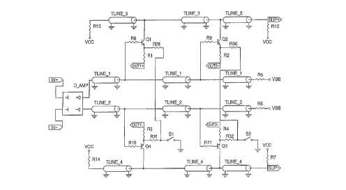
signal or at least a first part thereof from a first connection
point (IN+) in the input to a first transmission line
(TLINE_1); conducting the input signal or the first part
thereof selectively from said first transmission line to a
first connection point (OUT1+) in one of at least two outputs
(OUT1+, OUT1-, OUT2+, OUT2-) on the demultiplexer via a first
controllable signal forwarding device (Q1) as an output signal
or a first part of an output signal of high signal quality.

2. A method according to Claim 1, characterized by conducting
the input signal or the first part thereof to a third
transmission line (TLINE_3) at the same time as said input
signal or said first part thereof is conducted to said first
connection point (OUT1+) in the output, such as to create a
first replica of the output signal or the first part thereof.

3. A method according to Claim 1 or Claim 2, characterized in
that the input signal includes a first and a second part,
wherein the second part of the input signal is conducted,
simultaneously with the first signal part, from a second
connection point (IN-) in the input to a second transmission
line (TLINE_2) and the second part is thereafter conducted from
said second transmission line to a second connection point
(OUT1-) in said one output, via a second controllable signal
forwarding device (Q4).

4. A method according to Claim 3, characterized by conducting
said second part of the input signal to a fourth transmission

14
line (TLINE_4) at the same time as said second part is
conducted to said second connection point (OUT1-), such as to
generate a second replica of the second part of said output
signal.

5. A method according to any one of the preceding Claims,
characterized by amplifying the input signal prior to
conducting said signal to the transmission lines (TLINE_1,
TLINE_2) which together bind the input to said one output.

6. A demultiplexer having an input (IN+, IN-) and at least
two outputs (OUT1+, OUT1-, OUT2+, OUT2-), wherein a first
connection point (OUT1+, OUT2+) in each output is connected to
a common line (TLINE_1) via a respective first controllable
signal forwarding device (Q1, Q2), wherein said first connection
point in each output is also connected to an externally
controlled switch (S1, S2) which functions to control said
first signal forwarding device to forward a signal or a first
part of a signal applied through the common line to the first
connection point in said output, characterized in that the
common line is a first transmission line (TLINE_1) which is
also connected to a first connection point (IN+) in the input.

7. A demultiplexer according to Claim 6, characterized in
that each first signal forwarding device (Q1, Q2) is also
connected to a third transmission line (TLINE_3) for generating
a monitoring signal or a first part of a monitoring signal.

8. A demultiplexer according to Claim 6 or Claim 7,
characterized in that a second connection point (OUT1-, OUT2-)
in each output is connected to a second transmission line
(TLINE_2) via a respective second controllable signal
forwarding device (Q4, Q3), wherein said second transmission


line is connected to a second connection point (IN-) in the
input, and wherein said switch (S1, S2) also controls said
second signal forwarding device.

9. A demultiplexer according to Claim 8, characterized in
that each second signal forwarding device (Q3, Q4) is also
connected to a fourth transmission line (TLINE_4) for
generating a second part of a monitoring signal.

10. A demultiplexer according to any one of Claims 6-9,
characterized in that each of said transmission lines (TLINE_1,
TLINE_2, TLINE_3, TLINE_4) is a microstrip mounted in the
demultiplexer circuit board.

11. A demultiplexer according to any one of Claims 6-9,
characterized in that each of the transmission lines (TLINE_1,
TLINE_2, TLINE_3, TLINE_4) is a parallel plane conductor
mounted in the demultiplexer circuit board.

12. A demultiplexer according to any one of Claims 6-11,
characterized by an amplifier connected between the input
(IN1+, IN1-) and said transmission lines (TLINE_1, TLINE_2)
that connect the input with each output (OUT1+, OUT1-, OUT2+,
OUT2-).

13. A demultiplexer according to Claim 7 or Claim 9,
characterized in that the signal forwarding devices (Q1, Q4,
Q2, Q3) are transistors, wherein the emitter is connected to
the connection point in the output (OUT1+, OUT1-, OUT2+, OUT2-)
via a resistor (R1, R3, R2, R4), the base is connected to the
transmission lines (TLINE_1, TLINE_2) that connect the input
(IN+, IN-) with each output, and the collector is connected to

16
the transmission lines (TLINE_3, TLINE_4) so as to generate the
monitoring signal.
14. A demultiplexer according to any one of Claims 6-13,
characterized in that the transmission lines (TLINE_1, TLINE_2,
TLINE_3, TLINE_4) are terminated with a respective resistor
(R5, R6, R12, R13, R7, R14).

15. A protection switch unit (4) including a demultiplexer,
which has an input (IN+, IN-) and at least two outputs (OUT1+,
OUT1-, OUT2+, OUT2-), wherein a first connection point (OUT1+,
OUT2+) in each output on the demultiplexer is connected to a
common line (TLINE_1) via a respective first controllable
signal forwarding device (Q1, Q2) wherein also connected to
each output is an externally controllable switch means (S1, S2)
which functions to control said first signal forwarding device
to forward to the first connection point in the output a signal
or a first part of a signal applied over the common line or
conductor, characterized in that the common line (TLINE_1) is a
first transmission line which is also connected to a first
connection point (IN+) in the input of the demultiplexer.

16. A unit (4) according to Claim 15, characterized in that
each first signal forwarding device (Q1, Q2) is also connected
to a third transmission line (TLINE_3) so as to generate a
monitoring signal or a first part of a monitoring signal.

17. A unit (4) according to Claim 15 or Claim 16, characterized
in that a second connection point (OUT1-, OUT2-) in each
demultiplexer output is connected to a second transmission line
(TLINE_2) via a respective second controllable signal
forwarding device (Q4, Q3), wherein the second transmission
line is connected to a second connection point (IN-) in the


17

input, and wherein said switch means (S1, S2) also control said
second signal forwarding devices.

18. A unit (4) according to Claim 17, characterized in that
each second signal forwarding device (Q3, Q4) is also connected
to a fourth transmission line (TLINE_4) so as to generate a
second part of a monitoring signal.

19. A unit (4) according to any one of Claims 15-18,
characterized by an amplifier connected between the input
(IN1+, IN1-) and the transmission lines (TLINE_1, TLINE_2) that
connect the input with each demultiplexer output (OUT1+, OUT1-,
OUT2+, OUT2-).

20. A unit (4) according to Claim 16 or Claim 18, characterized
in that the signal forwarding devices (Q1, Q4, Q2, Q3) are
transistors, wherein the emitter is connected to the connection
point in respective outputs (OUT1+, OUT1-, OUT2+, OUT2-) via a
respective resistor (R1, R3, R2, R4), wherein the base is
connected to the transmission line (TLINE_1, TLINE_2) that
connects the input (IN+, IN-) with each output, and wherein the
collector is connected to the transmission line (TLINE_3,
TLINE_4) so as to generate the monitoring signal.

21. A unit (4) according to any one of Claims 15-20,
characterized in that the transmission lines (TLINE_1, TLINE_2,
TLINE_3, TLINE_4) in the demultiplexer are terminated with a
respective resistor (R5, R6, R12, R13, R7, R14).

22. A telecommunications network that includes two or more
lines connected to an exchange (1) via a respective terminal
access unit (3), wherein each line is also connected to a
protection switch unit (4) which, in turn, is connected to the

18

exchange via a reserve terminal access unit (5), wherein the
protection switch unit includes a demultiplexer that has an
input (IN+, IN-) and at least two outputs (OUT1+, OUT1-, OUT2+,
OUT2-), wherein a first connection point (OUT1+, OUT2+) in each
demultiplexer output is connected to a common line (TLINE_1)
via a respective controllable signal forwarding device (Q1,
Q2), wherein each output is also connected to an externally
controlled switch means (S1, S2) for controlling said first
signal forwarding device to forward to the first connection
point in the output a signal or a first part of a signal which
is applied over the common line, characterized in that the
common line (TLINE_1) is a first transmission line which is
also connected to a first connection point (IN+) in the
demultiplexer input.

23. A telecommunications network according to Claim 22,
characterized in that each first signal forwarding device (Q1,
Q2) is also connected to a third transmission line (TLINE_3) so
as to generate a monitoring signal or a first part of a
monitoring signal.

24. A telecommunications network according Claim 22 or Claim
23, characterized in that a second connection point (OUT1-,
OUT2-) in each demultiplexer output is connected to a second
transmission line (TLINE_2) via a respective second controllable
signal forwarding device (Q4, Q3) which is connected to a
second connection point (IN-) in the input, wherein said switch
means (S1, S2) also controls said second signal forwarding
device.

25. A telecommunications network according to Claim 24,
characterized in that each second signal forwarding device (Q3,

19


Q4) is also connected to a fourth transmission line (TLINE_4)
so as to generate a second part of a monitoring signal.

26. A method relating to demultiplexing for selecting one of a
plurality of outputs as an output for an input signal received
on an input, comprising the steps of:
- conducting the input signal or at least a first part of said
signal from a first connection point in the input to a first
transmission line; and
- conducting the input signal for the first part of said signal
from the first transmission line to a first connection point in
one of at least two demultiplexer outputs via a first
controllable signal forwarding device as an output signal for a
first part of an output signal that has good signal quality.

27. A demultiplexer that has an input and at least two
outputs, wherein a first connection point in each output is
connected to a common line via a respective first controllable
signal forwarding device; wherein there is also connected to
each output an externally controlled switch means which
functions to control the first signal forwarding device to
forward to the first connection point in said output a signal
or a first part of a signal that is applied over the common
line; and wherein the common line is a first transmission line
which is also connected to a first connection point in the
input.

28. A protection switch unit comprising a demultiplexer which
has an input and at least two outputs, wherein a first
connection point in each demultiplexer output is connected to a
common line via a respective first controllable signal
forwarding device; wherein there is also connected to each


output an externally controlled switch means which functions to
control said first signal forwarding device to forward to the
first connection point in the output a signal or a first part
of a signal applied over the common line; and wherein the
common line is a first transmission line which is also
connected to a first connection point in the demultiplexer
input.

29. A telecommunications network comprising two or more lines
which are connected to an exchange via a respective terminal
access unit, wherein each line is also connected to a
protection switch unit which, in turn, is connected to the
exchange via a reserve terminal access unit, wherein the
protection switch unit includes a demultiplexer which has an
input and at least two outputs, wherein a first connection
point in each demultiplexer output is connected to a common
line via a respective first controllable signal forwarding
device; wherein there is also connected to each output an
externally controlled switch means which functions to control
said first signal forwarding device to forward to the first
connection point in said output a signal or a first part of a
signal applied over the common line; and wherein the common
line is a first transmission line which is also connected to a
first connection point in the demultiplexer input.

Description

Note: Descriptions are shown in the official language in which they were submitted.


CA 02222624 1997-11-27
W O 96138943 PCTI~E96100679

DEMULTIPLEXER, A PRO ~ ON SWlTCH UNIT, A TELECOMMUNICATION NElWORK AND
A MErHOD OF DEMULTIPLEXING

FIE~D OF INVENTION

The present invention relates to a demultiplexer, a protection
switch unit which includes one such demultiplexer, a
telecommunications network which includes one such protection
switch unit, and a method relating to demultiplexing. More
specifically, the invention relates to the aforesaid apparatus
and method in respect of demultiplexing signals that are
single-mode or differential-mode signals and preferably of the
CMI type at transmission speeds above about 100 Mbit/s and
preferably i~ the range of about 140-155 Mb/s.

DESCRIPTION OF THE BACKGROUND ART

In telecommunications networks, a plurality of signal lines are
often connected to an exchange through the medium of a
respective terminal access unit. These terminal access units
are relatively expensive and complicated units, which can
sometimes break down. For this reason, the network includes at
least one protection switch unit which includes a demultiplexer
whose outputs are connected to the signal lines and whose input
is connected to the reserve terminal access unit.

When a standard terminal access unit cannot be used for some
reason or another, the exchange sends to the demultiplexer of
the protection switch unit output signals which are intended
for the signal line connected to the unusable normal terminal
access unit via the reserve terminal access unit, said
demultiplexer being controlled to forward the output signal to
said signal line.

. CA 02222624 1997-11-27
W 096/38943 PCT/SE96/00679

Good signal quality is required when switching or demulti-ple-
xing signals having transmission speeds in the region of about
140-155 Mb/s. In this regard, the pulse shape of the output
signal is often required to be the same as the pulse form of
the input signal.

Problems with mismatching between components and conductors can
easily occur in such demultiplexers at such high transmission
speeds, therewith greatly impairing signal quality.

It is also often necessary to monitor the reserve terminal
access unit and also possibly the demultiplexer in the
protection switch unit with regard to faults.

A plurality of standard circuits exist for demultiplexing
signals having bit rates of up to about 30 Mb/s, in a
relatively simple and inexpensive manner. At higher bit rates,
line impedances, connections, terminations, line runs and
component data place strict requirements on circuitry. In order
to keep conductor~impedances as constant as possible, it is
necessary to take particular care in implementing the printed
board assembly.

The circuitry using standard circuits in a demultiplexer is
expensive and highly current consuming.

There is no technique at present for effectively demultiplexing
while monitoring in the aforesaid transmission speed ranges.
Neither is there known a demultiplexer which will a~ford
monitoring of the input signal at the same time.

US-A 5,146,113 describes an integrated circuit having several
narrow, elongated resistance strips on a circuit board, to

' CA 02222624 1997-11-27
W 096138943 PCT/SE96100679


provide a board-mounted circuit with a predetermined input
and/or output impedance.

US-A 5,281,934 describes a microwave multiplexor which is
entirely of microstrip construction.

SU~ME~RY OF THE INVENTION


One object of the present invention is to provide a method of
selecting one of several outputs as the output of a received
input signal when demultiplexing, therewith obtaining good
signal quality in a simple and inexpensive manner at the same
time.

This object is achieved with a method in which an input signal
received on an input is first conducted to a first transmission
line and thereafter selectively to one of at least two outputs.

Another object of the invention is to provide a method of
selecting one of several outputs as the output of a received
input signal when demultiplexing, and of enabling a signal
transferred to one of the outputs to be monitored in a simple
manner.

This object is achieved with a method which also includes
generating a replica of the signal forwarded to a selected
output by, at the same time, conducting the input signal that
was passed to the selected output to a third transmission line.

A further object of the invention is to provide a method of
selecting one of several outputs as the output for a received
input signal when demultiplexing, where distortion in the
signal obtained on the selected output and on the replica of
this signal can be reduced readily in a later stage.

CA 02222624 1997-11-27
WO 96/38943 PCT/SE96/00679


This object is realized with a method in which the input signal
includes two parts and the two parts of said input signal are
each conducted to a respective first and second transmission
line and thereafter selectively conducted to a respective first
and second connection point in a selected output and also to a
respective third and fourth transmission line.

Still another object of the present invention is to provide a
demultiplexer, a protection switch unit including one such
demultiplexer, and a telecommunications network which includes
one such protection switch unit, where good signal quality is
obtained in a simple and inexpensive manner when selecting one
of several outputs as the output for a received input signal.

This object is achieved with a demultiplexer, a protection
switch unit and a telecommunications network wherein the
demultiplexer includes an input and at least two outputs,
wherein a connection point in the input is connected to a first
transmission line to which a first connection point in each
output is connected via a respective first controllable signal
forwarding conductor means.

Yet a further object of the invention is to provide a
demultiplexer, a protection switch unit which includes one such
demultiplexer, and a telecommunications network which includes
one such protection switch unit, wherein the function of the
demultiplexer and the function of the unit connected to the
input of the demultiplexer can be readily monitored.

This object is achieved with a demultiplexer, a protection
switch unit and a telecommunications network wherein each first
signal forwarding conductor means is connected to a third
transmission line.

' CA 02222624 1997-11-27
W 096/38943 PCTISE96/00679

Still yet a further object of the invention is to provide a
demultiplexer, a protection switch unit that includes one such
demultiplexer and a telecommunications network that includes
one such protection switch unit, wherein distortion obtained in
output signals from the demultiplexer can be readily reduced in
later stages.

This object is achieved with a demultiplexer, a protection
switch unit and a telecommunications network wherein a second
connection point in the demultiplexer input is connected to a
second transmission line which, in turn, is connected to a
second connection terminal in each output via a respective
second controllable signal forwarding conductor means, which
may optionally also be connected to a fourth transmission line.

BRIEF DESCRIPTION OF THE DR~WINGS


Further objects of the invention and advantages afforded
thereby will be evident from the following description of a
preferred embodiment of the invention made with reference to
the accompanying drawings, in which

Fig. 1 is a block schematic of an inventive telecommunications
system; and

Fig. 2 is a circuit diagram of an inventive demultiplexer.

DE~TT-~.n DESCRIPTION OF A ~K~KK~ EM3ODIM~NT


Fig. 1 is a block schematic of a telecommunications system
which operates with CMI signals transmitted at transmission
speeds in the range of about 140-155 Mb/s. This system includes
an exchange 1 which communicates with a plurality of signal
conductors. Each signal conductor is connected to a protection
.

CA 02222624 1997-11-27
W 096/38943 PCT/SE96/00679

unit 2 (PU = Protection Unit). Although only eight protection
units are shown in Fig. 1, it will be understood that these
units may be fewer or more in number. Signals incoming to and
outgoing from the protection units 2 are denoted with arrows
that point towards and away from respective units 2. Each
protection unit 2 is connected to the exchange 1 via a
respective terminal access unit 3 (TAU), of which only eight
are shown although these units will actually be sixteen in
number. The modus operandi of these terminal access units 3
plays no part in the present invention and is well known to the
person skilled in this art and need not therefore be explained
in great detail. It should be mentioned, however, that these
terminal access units 3 are relatively complicated and
expensive and have such a high fault frequency as to
necessitate some form of protective switch. In order to avoid a
signal conductor becoming unusable, there is provided a reserve
terminal access unit 5 which when one of the regular terminal
access units 3 is inoperative is switched-in to replace this
unit. The reserve terminal access unit 5 is connected between
the exchange 1 and a protection switch unit 4 (PSU).

This protection switch unit is connected to each protection
unit 2. The main duty of the protection units 2 is to convert
single-mode signals incoming to the protection switch unit ~
into differential-mode signals, and to convert differential-
mode signals outgoing from the exchange 1 via the terminalacces~ units 3 and the protection switch unit 4 to single-mode
signals. The protection switch unit 4 includes a multiplexor or
selector and a demultiplexer. The multiplexor functions to
receive all of the signals incoming on the conductors and to
selectively forward one of said signals, and the demultiplexer

.
CA 02222624 1997-11-27
W 096/38943 PCT/SE96/00679

functions to receive a signal outgoing from the exchange 1 and
to forward this signal to a selected signal conductor.

Fig. 2 illustrates an embodiment of an inventive demultiplexer,
wherein only two outputs are shown for the sake of simplicity,
although it will be understood that the demultiplexer will
normally include many more outputs. A first of the outputs has
a first and a second connection point OUT1+ and OUT-. The first
connection point OUT1+ of the first output is connected to a
first signal forwarding conductor means Q1 via a resistor R1,
said means Q1 being connected to an RF transistor in the
illustrated case. The resistor R1 is connected to the emitter
of the transistor Q1 in the illustrated case. The transistor
base is connected via a resistor R8 to a first transmission
line TLINE_1. One end of the transmission line TLINE_1 is
terminated with a resistor R5 which is connected to a voltage
source VBB.

The transistor collector is connected to a third transmission
line TLINE_3 included in the demultiplexer circuit board, said
third transmission line being terminated at both ends with
respective resistors R13 and R12 connected to a voltage source
VCC, said voltage source optionally being the same as VBB. A
first connection point SUP+ is provided in an output for
monitoring signals at one end of the third transmission line
TLINE_3.

The second connection point OUT1- of the first input is
connected to a second transmission line TLINE_2 mounted on the
demultiplexer circuit board via a resistor R3, and RF
transistor Q4 and a further resistor R10, similar to the first
connection point OUT1+. One end of the TLINE_2 is terminated
.

CA 02222624 1997-11-27
W O 96t38943 PCT/SE96/00679


with a resistor R6 which is connected to the voltage source
VBB. The collector of the transistor Q4 is connected to a
fourth transmission line TLINE_4 mounted on the demultiplexer
circuit board, this fourth transmission line being terminated
with a resistor R14 at one end and a resistor R7 at the other
end in a manner similar to the third transmission line TLINE_3,
said resistors being connected to the voltage source VCC. A
second connection point in the monitoring signal output is
obtained at one end of the fourth transmission line TLINE_4.

Respective emitters of the first and second transistors Q1 and
Q4 are connected to one end of a first externally controlled
switch means S1 via a resistor R29 and R31 respectively. The
other end of the switch S1 is connected to earth.

The connection points OUT2+ and OUT2- of a second output are
connected to the first and the second transmission lines
TLINE_1 and TLINE_2 respectively in exactly the same way, via a
resistor R2, a transistor Q2 and a resistor R9, and via a
resistor R4, a transistor Q3 and a resistor R11. Respective
collectors of the transistors Q2 and Q3 are connected to the
third and the fourth transmission lines TLINE_3 and TLINE_4
respectively. Respective emitters of the transistors Q2 and Q3
are connected to a second externally controlled switch S2 via
resistors R30 and R32 in exactly the same ~ay as the first
output, said switch S2 also being connected to earth similar to
the switch S1.

The transistors Q1, Q2, Q3 and Q4 and associated components are
so placed along the transmission lines TLINE_1, TLINE_2,
TLINE_3 and TLINE_4 that mismatches and reflexions will be
minimal. In reality, further transistors for further outputs

' CA 02222624 1997-11-27
W O 96/38943 PCT/SE96/00679

are correspondingly placed along said transmission lines
TLINE_1, TLINE_2, TLINE_3 and TLINE_4.

A differential amplifier D_AMP has one output and is connected
to the first transmission line TLINE_1 at a first connection
point +0 therein and to the second transmission line TLINE_2 at
a second connection point -0. The amplifier D_AMP has an input
having two connection points +I and -I which are each connected
to a respective connection point IN+ and IN- in the input.

Resistors that terminate the ends of respective first and
second transmission lines TLINE_1 and TLINE_2 where the
amplifier D_AMP is connected are included in this amplifier and
are also connected to the source VBB, which is also included in
the amplifier D_AMP at this end of the transmission lines and
is not therefore shown in the Figure.

In the preferred embodiment, each of the transmission lines
TLINE_1, TLINE_2, TLINE_3 and TLINE_4 has the form of a
microstrip included in the board circuitry and to which the
transistors are connected. These microstrips are preferably
rectilinear, have identical lengths and are essentially of
unitary width. An important feature of this embodiment,
however, is that the two transistors at each output have
equally long paths to the connection points +0 and -0 in the
output of the amplifier D_AMP. The transmission lines TLINE_1,
TLINE_2, TLINE_3 and TLINE_4 may optionally be slightly
narrower at those points where the transistors are connected,
so as to match the impedance of a microstrip to the additional
capacitance that is supplied by a passive transistor.
Alternatively, the impedances of respective transmission lines
can be matched to the capacitances of the passive transistors

CA 02222624 1997-11-27
W 096/38943 PCT/SE96/00679
-

by choosing the value of the terminating resistors R5, R6, R7,
R12, R13 and R14 to correspond to the transmission lines having
the additional distributed capacitances that the transistors
supply.

Another conceivable variant of the transmission lines are
parallel plane lines (stripline) disposed in intermediate
layers of the circuit board. This transmission line embodiment,
however, would require the transistors to be connected to said
lines by means of bushings or throughlets, which would make the
matching problem slightly more difficult to resolve than when
the transistors are connected to a microstrip. However, the
inputs and outputs of the demultiplexer are often arranged in
the form of parallel plane lines that extend through the
interior of the circuit board.

The demultiplexer illustrated in Fig. 2 functions with
differential-mode signals, which results in less distortion in
the signals leaving the demultiplexer. The demultiplexer
operates as follows: An input signal is received on the input
IN+, IN- and amplified to an appropriate level in the amplifier
D_AMP. The amplified input signal is forwarded to a selected
output by the first and the second transmission lines TLINE_1,
TLINE_2. The amplification of the amplifier D_AMP is chosen so
as to essentially compensate for subsequent losses due to
output impedance and load.

One of the outputs, such as the first output for instance, is
activated by the first externally controlled switch S1, which
activates the transistors Q1 and Q4 connected to the input when
said input is closed. The second input is passive, i.e. the
second switch S2 is off.

CA 02222624 1997-11-27
W 096/38943 PCTISE96/00679
- 11


The switches may comprise any one of a number of different
designs known to the person skilled in this art, for instance
transistors. The switches S1 and S2 are controlled by a control
circuit arranged in the protection switch unit and functioning
to close a switch depending on which of the aforesaid terminal
access units is inoperative. This switching function may also
be accomplished directly from the aforesaid exchange. Closing
of the switch S1 results in biassing of the transistors Q1 and
Q4 and the amplified input signal is conducted from the
transmission lines TLINE_1 and TLINE_2 through the transistors
Q1 and Q4 and to the connection points OUT1+ and OUT1- in the
first output.


The demultiplexer is adapted to conduct an output signal also
to the third and the fourth transmission lines TLINE 3 and
TLINE_4 immediately when the output signal i5 obtained on an
output. This means that a replica of the input signal is also
obtained. This replica is obtained on the connection points
SUP+, SUP- of the monitoring output and is processed in a
monitoring circuit, which may be included in the protection
switch unit. The demultiplexer may also include a second
differential amplifier for amplifying the monitoring signal. It
can be established whether or not the reserve access unit is
broken or not, by analyzing this signal. An analysis of the
signal will also reveal whether or not the demultiplexer is
working in the manner intended. This represents a saving in the
additional monitoring circuits that would otherwise be
- required.


The connection of the transmission lines means that any
reflexions therein will be quickly extinguished. The trans-

mission lines are arranged so that the third and the fourth

CA 02222624 1997-11-27
W 096/38943 12 PCT/SE96/00679

transmission lines TLINE_3 and TLINE_4 have roughly half the
impedance of the first and the second transmission lines
TLINE_l and TLINE_2. This is achieved by virtue of selecting
the width of the transmission lines and their respective
distances to the earth plane. As a result of such selection,
the collector voltage on a transistor will be lower than the
emitter and the base voltage. Crosstalk from collector to base
will therefore have only a very slight influence on signal
quality. A certain degree of crosstalk may occur in the reverse
direction, from base to collector, but the quality of the
monitoring signal is not equally as important as the quality of
the output signal. Since the collector voltage is low in
comparison wi~th the base and emitter voltage, the transistor
can be considered as an emitter follower. This gives a high
input impedance and therewith has little influence on the first
and the second transmission lines TLINE_1 and TLINE_2, which
has only a slight effect on the pulse shape.

The amplifier D_AMP may alternatively be connected to the
opposite end of the first and the second transmission lines
TLINE_l and TLINE_2. The monitoring signal output may also be
placed at the opposite end of the third and fourth transmission
lines TLINE_3 and TLINE_4.

Representative Drawing
A single figure which represents the drawing illustrating the invention.
Administrative Status

For a clearer understanding of the status of the application/patent presented on this page, the site Disclaimer , as well as the definitions for Patent , Administrative Status , Maintenance Fee  and Payment History  should be consulted.

Administrative Status

Title Date
Forecasted Issue Date Unavailable
(86) PCT Filing Date 1996-05-24
(87) PCT Publication Date 1996-12-05
(85) National Entry 1997-11-27
Dead Application 2001-05-24

Abandonment History

Abandonment Date Reason Reinstatement Date
2000-05-24 FAILURE TO PAY APPLICATION MAINTENANCE FEE

Payment History

Fee Type Anniversary Year Due Date Amount Paid Paid Date
Registration of a document - section 124 $100.00 1997-11-27
Application Fee $300.00 1997-11-27
Maintenance Fee - Application - New Act 2 1998-05-25 $100.00 1998-05-14
Maintenance Fee - Application - New Act 3 1999-05-25 $100.00 1999-05-10
Owners on Record

Note: Records showing the ownership history in alphabetical order.

Current Owners on Record
TELEFONAKTIEBOLAGET LM ERICSSON
Past Owners on Record
BLADH, MATS
Past Owners that do not appear in the "Owners on Record" listing will appear in other documentation within the application.
Documents

To view selected files, please enter reCAPTCHA code :


To view images, click a link in the Document Description column. To download the documents, select one or more checkboxes in the first column and then click the "Download Selected in PDF format (Zip Archive)" or the "Download Selected as Single PDF" button.

List of published and non-published patent-specific documents on the CPD .

If you have any difficulty accessing content, you can call the Client Service Centre at 1-866-997-1936 or send them an e-mail at CIPO Client Service Centre.


Document
Description 
Date
(yyyy-mm-dd) 
Number of pages   Size of Image (KB) 
Representative Drawing 1998-03-23 1 9
Abstract 1997-11-27 1 27
Description 1997-11-27 12 499
Claims 1997-11-27 8 322
Drawings 1997-11-27 2 36
Cover Page 1998-03-23 2 75
PCT 1997-11-27 34 1,234
Assignment 1998-10-27 2 76
Correspondence 1998-10-27 1 41
Assignment 1997-11-27 4 170
Assignment 1997-11-27 3 129
Correspondence 1998-02-24 1 31