Note: Descriptions are shown in the official language in which they were submitted.
CA 02222637 1997-11-28
MONOSTATIC RADAR SYSTEM HAVING A ONE-PORT
IMPEDANCE MATCHING DEVICE
This application is a division of Canadian Patent
Application No. 2,140,936 filed January 24, 1995.
BACKGROUND OF THE lNV~N-LlON
This invention relates generally to obstacle detection and
ranging systems and more specifically to near range obstacle
detection systems. The following are a few of the applications
in which such a near range obstacle detection system may be used:
~ Vehicular obstacle detection and headway control
~ Autonomous tele-operated vehicle obstacle detection
~ Space robotics
~ Control of work platforms and forklifts
~ Terrain mapping through vegetation
~ Weapons fusing
~ Battlefield surveillance
~ Tank gauging (determining the amount of a substance
stored in a container)
~ Marine vessel docking and guidance
~ Airplane auto-docking
~ Personnel bridge docking
~ Airport runway incursion
~ Altimeter
~ Presence sensor for traffic light control
~ Ice thickness measurement
~ Pavement thickness measurement
~ Buried object detection
~ Underground tunnel or void detection
~ Perimeter security surveillance
~ Aid to the handicapped
Some prior art near obstacle detection systems utilize
infrared and ultrasonic radiation. These systems generally have
disadvantages that discourage their use.
Microwave radiation on the other hand is commonly used in
a variety of forms of radar systems, and the advantages of
CA 02222637 1997-11-28
--2--
microwave radar technology make it attractive for near obstacle
detection systems as well. See the article "Automotive Radar:
A Brief Review " by D.M. Grimes and T.O. Jones in Proceedings of
the IEEE, June, 1974, pp. 804-822 and the relevant prior art
literature cited therein.
An important microwave operating band assigned for radar
use, generally designated as X-band, covers the frequency range
from 8.2 to 12.4 GHz. In this frequency range, microwave
components are reasonable in both size and cost. For example,
the dimensions of an X-band planar or patch antenna, suitable for
near obstacle detection, are approximately 1 inch x 2 inches.
A portion of X-band set aside by the Federal Communications
Commission for unlicensed use covers the frequency range from
10.50 to 10.55 GHz. However, this limited bandwidth makes it
difficult to achieve adequate resolution for nearby targets. For
example, with a conventional frequency modulated-continuous wave
(FM-CW) radar system operating over a 50 MHz bandwidth, the
minimum resolution is approximately 10 feet, whereas a resolution
of the order of inches is considered necessary for near obstacle
detection such as vehicular warning systems.
Where antenna mounting space is at a premium, it is
possible to utilize one antenna for both transmitting and
receiving. This one antenna system is called a monostatic radar
system. A major drawback of monostatic systems is the unwanted
presence of an internally reflected signal from the antenna.
Since the internally reflected signal may be an order of
magnitude larger than the reflected signal from the target, the
accurate detection of a target may not be possible in a narrow
band system since the receiver detects the composite signal
consisting of the internally reflected signal from the antenna
as well as the reflected signal from the target.
An analogous situation occurs in bi-static or two antenna
systems. The unwanted signal is due to the leakage between the
two antennas. However, this leakage signal is usually much
smaller than the reflected antenna signal in the monostatic
system. In most situations, the leakage signal can be ignored.
However, in some cases, an active two-port phase
. CA 02222637 1997-11-28
shifter/attenuator or I-Q modulator is employed. This two-port
device generates a signal of equal magnitude and opposite sign
to that of the leakage signal, cancelling the leakage signal.
OBJECT OF THE lNV~ lON
It is among the objects of this invention to provide a new
and improved system that can be utilized for near obstacle
detection, tank/container gauging and ice thickness measurement.
Another object is to provide a new and improved microwave
radar system useful as an obstacle detection system.
Another object is to provide a new and improved radar
system for use with limited frequency bandwidth and having a
sufficiently high resolution.
Another object is to provide a new and improved radar
system for detecting the closest obstacle among multiple
obstacles.
It is a further object to provide a monostatic radar
system that can be utilized for near obstacle detection,
tank/container gauging and ice thickness measurement.
SU~ RY OF THE lNv~NLloN
The present invention provides an improved monostatic
radar system for detecting near range obstacles and determining
their distance. An active one-port impedance-matching device (Z-
network) or I-Q modulator is employed. A generated signal is
directed to both the antenna and the device. The device reflects
a pre-determined portion of that signal with a pre-determined
phase change. The device cancels the reflected signal from the
antenna.
In accordance with this invention an obstacle detection
apparatus comprises: means for generating high frequency energy
over a finite frequency range and for frequency modulating over
a limited range of bandwidth such high frequency energy and for
supplying said frequency-modulated (FM) high frequency energy to
a first path providing a phase reference. A second path includes
CA 02222637 1997-11-28
transmission and receiving sections, and the transmission section
includes means for radiating the frequency modulated high
frequency energy into space in the form of propagating waves,
while the receiving section includes means for receiving a
portion of said radiated ener~y after reflection from a remote
object. The transmitting and receiving sections may be
physically separated, as in bistatic radar systems, or may have
a common antenna and signal path section as in monostatic
systems. The radiated energy portion acquires a phase shift
related to the distance traveled by said radiated energy and to
the frequency of the radiated energy. In one of said paths a
means serves to phase shift frequency-modulated high frequency
energy in that one path in a certain configuration of repeated
cycles of frequency modulation to improve resolution attainable
with said limited range of bandwidth. In the receiving section,
means for comparing the phase of FM energy with the phase of the
reflected radiated energy serves to produce signals related to
the phase-shifts of said first and second paths and corresponding
to the phase-shift produced over the distance travelled by the
radiated energy portion and the reflection thereof from the
remote object. A distance signal is derived in accordance with
the phase states of said phase shifter and related to the
frequencies of said energy generating and modulating means.
In accordance with an embodiment of this invention, the
means for deriving a distance signal includes, means for
transforming sinusoidal voltage wave from the time domain to the
frequency domain including means for performing a Fourier
analysis thereon. Also in accordance with an embodiment of this
invention, the phase-shifting means is in the reference path.
BRIEF DESCRIPTION OF THE DRAWINGS
The foregoing and other objects of this invention as well
as the invention itself may be more fully understood from the
following description when read together with the accompanying
drawings, in which corresponding parts are referenced by similar
numerals throughout, and in which:
~CA 02222637 1997-11-28
Fig. 1 is a schematic block diagram of a bi-static
obstacle detection and warning system embodying this invention.
Fig. 2 is a schematic graphical diagram of rotating
vectors illustrative of the operation of the system of Fi~. 1.
5 FigR. 3-0 through 3-F are 16 graphs (numbered
hexadecimally 0-F), schematic diagrams serving as an example of
signal data from the system of Fig. 1 and reconstructed in the
process of Fig. 4A.
FigQ. 4A and 4B are computer flow charts of the data
processing performed including the frequency transformation and
distance calculator.
Fig. 5 is a graphical diagram of a table of data
illustrating the operation of the distance calculator of Fig. 1
FigQ. 6A, 6B, and 6C are idealized timing and waveform
diagrams illustrating the operation of parts of the system of
Fig. 1.
Figs. 7, 8, and 9 are schematic block diagrams of modified
forms of the invention.
Fig. 10 is a schematic diagram showing zones in which
targets subject to monitoring are located in relation to an over-
the-road vehicle.
Fig. 11 is a schematic diagram of a typical monostatic
radar system.
Fig. 12 is a schematic diagram of a monostatic radar
system embodying the one-port Z-matching device of this
invention.
Fig. 13 is a schematic diagram of the temperature
uncompensated design of the one-port Z-matching device.
Fig. 14a is the parasitic and temperature compensated
design of the one-port Z-matching device.
Fig. 14b is the temperature compensated voltage generator.
Fig. 15 is the schematic diagram of a balanced monostatic
radar system embodying this invention.
CA 02222637 1997-11-28
Fig. 16 is the schematic diagram of a balanced monostatic
radar system utilizing two one-port matching devices.
Fig. 17 is a schematic diagram of the monostatic system
using an unbalanced Z-matching device.
Fig. 18 is a schematic diagram using a temperature
compensated balanced Z simulator.
Fig. 19 is a schematic block diagram of a monostatic radar
system embodying this invention.
Fig. 20 is a schematic block diagram showing a typical
frequency modulated continuous wave (FM-CW) radar system.
Fig. 21 is a schematic block diagram showing a modified
frequency modulated-continuous wave (FM-CW) radar system.
DETAILED DESCRIPTION OF THE lNV~NLlON
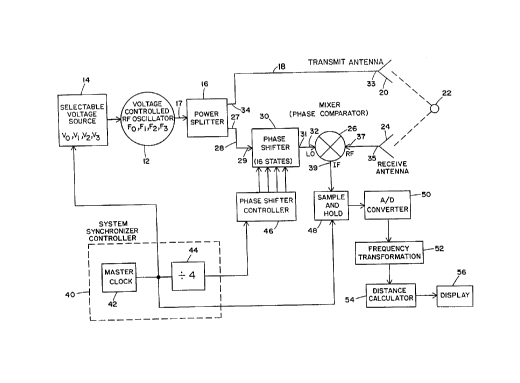
In the system 10 of Fig. 1 for radar ranging, a voltage-
controlled oscillator 12 (VCO) generates the basic RF signal as
a continuous wave (CW) with a periodic frequency modulation (FM)
superimposed in accordance with a periodic modulating voltage
from a selectable source 14.
The RF voltage from the VCO 12 is applied via a power
splitter 16 and transmitting RF path 18 to a transmitting antenna
20. The latter radiates a corresponding electromagnetic wave to
a remote target 22, and the radiation reflected from the target
returns to a receiving antenna 24. The reflected RF signal is
supplied to the RF input of a mixer 26. Another RF path 28 from
the power splitter 16 supplies the FM-CW signal to a phase
shifter 30, which shifts the phase of that signal in a certain
periodic configuration and applies the phase-shifted signal to
the LO (local oscillator) input 32 of the mixer 26.
Voltage Controlled Oscillator - The frequency of the VCO
12 is determined by the applied control voltages V0, Vl, V2, V3,
from the source 14 and can be varied over the operating band in
CA 02222637 1997-11-28
several ways. Among them are:
a. Continuously increasing or decreasing frequency over
a fixed period T. This is usually referred to as a linear
frequency-modulated continuous wave (linear FM-CW) signal. This
type of frequency modulation can be used with either an analog
or digital signal processing system.
b. Step-wise increasing frequency is preferable for the
digital signal processing approach. For optimum signal
processing efficiency, the generated frequencies should be
equally spaced.
The present best mode of the invention uses the step-wise
frequency modulation scheme. Four frequencies are generated
during each period. They are spaced 12.5 MHz apart, beginning
at 10.5 GHz and ending at 10.5375 GHz. Each frequency state is
energized for a period of 0.02 msec. Therefore, each frequency
sweep period has a 0.08 msec duration as shown in Figs. 6A
through 6C.
Power Splitter - The power splitter 16 is a 3-port device
(e.g. a Wilkinson power divider or a quadrature coupler with the
isolated port terminated). The energy of the signal at the input
port 17 is split equally between output ports 27 and 34. The
phase difference between the signals at these ports must not
change significantly for any of the frequencies at which the
system operates. The actual value of the phase difference is not
important to the function of the system.
Transmitting and Receiving Antennas - The signal
energizing the transmitting antenna 20 at its input port 33 is
transmitted with a directional pattern determined by the geometry
of the antenna. Part of the signal is scattered with an
undetermined pattern and amplitude from an object 22. Some of
that scattered energy will appear at the receiving antenna 24 and
is available at port 35. The amplitude of the received signal
depends on (i) the directional (gain) patterns of both antennas,
(ii) the transmitting range from antenna 20 to target 22, (iii)
the scattering characteristics of the target 22 and (iv) their
CA 02222637 1997-11-28
range from target 22 to receiving antenna 24.
The directional patterns of both antennas 20 and 24 and
their relative location and orientation should be such that the
magnitude of the leakage signal propagating directly between the
antennas, that is between the points 33 and 35, should be
.
mlnlmlzed.
Mixer - The mixer 26 (or phase comparator) can be either
a 2-or 3-port device. The latter version has been employed in
the present embodiment. The 3-port device (e.g. a double
balanced mixer) has reference, input and output ports 32, 37 and
39, respectively. They are also commonly referred to as the LO,
RF and IF ports respectively. (In the 2-port device, e.g., a
single-balanced mixer, the LO, and RF ports use a single port).
In this embodiment, the function of the mixer 26 is
essentially that of a "two-quadrant" phase comparator. As such,
the voltage at output port 39 IF is a sinusoidal function of the
phase difference between ~ref ~ the phase of the voltage at the
reference point 32, and ~inpl the phase of the voltage at the
input port 37. Mathematically, this function is:
VOUt = a sin(~ref ~ ~inp) + b
where "a" is device-dependent voltage scaling factor, and "b" is
a fixed residual offset voltage. For the purpose of
demonstrating the function of the system, the residual offset
voltage can be assumed to be zero. Consequently, if the voltages
at the input and output ports are either in phase (0~ difference)
or out of phase (180~ difference), then the voltage at the output
port will be zero. Likewise for phase differences of +90~ and
-90~ the output voltages are +a and -a respectively. For all
other phase differences, the output voltage varies between +a and
-a in a sinusoidal fashion.
Phase Shifter - The phase shifter 30 is an insertable 2-
port device. With the device energized at the input port 29, the
CA 02222637 1997-11-28
phase of the RF voltage at the output port 31 can be changed by
means of a signal applied to the control port. The range over
which the phase can be changed is 360~, and it can be changed
either continuously, as in an analog phase shifter, or in a fixed
number of steps, as in a digitally controlled phase shifter. For
a fixed control signal, the phase change must not vary
significantly over the system operating band.
In this embodiment of the radar system, the phase shifter
30 is digitally controlled. The phase of the signal at the
output port can be set to any one of the 16 equally spaced 22.5~
steps by means of a 4-bit digital control signal.
D/A Selectable Voltaqe Source - The selectable voltage
source 14 sequentially applies one of four voltages to the VCO,
each for a 0.02 msec duration. For a single operating period,
the sequence of four voltages is repeated 16 times for a total
duration of 1.28 msec. The timing is controlled by the system
synchronizer/controller 40.
Phase Shifter Controller - The phase shifter controller
46 applies a 4-bit digital signal to the phase shifter 30. Each
of the possible 16 phase steps lasts for a period of 0.08 msec,
synchronized with the A/D selectable voltage source by means of
the system synchronizer/controller. The total time interval
required for all 16 phase states is 1.28 msec.
A/D Converter/Sampler - The A/D converter/sampler 50
samples the voltage at the output port of the mixer 26 every 0.02
msec and converts the sampled voltage into a 12-bit digital
number (-2046 to +2045). A total of 64 samples is taken during
the 1.28 msec period. The sampled data are stored in a digital
form in Random Access Memory (RAM) for further signal processing.
System Synchronizer/Controller - The system synchronizer/
controller's 40 function is to synchronize the three control
components described above. A total of 64 data points is taken,
which can be divided into 16 sequences of 4 data points, each
sequence associated with one of the 16 phase states. The
sequences can therefore be designated by their phase states. (A
master clock 42 sets the basic repetition rate of the voltage
, , CA 02222637 1997-11-28
-10-
source 14 with its clock signals divided down by counter 44, the
repetition rate for the 16 phase states is set.)
The total acquisition time of the 64 data points is 1.28
msec. In the automotive application, where maximum relative
speed between the antennas and an object does not exceed 12
inch/msec, any object can be considered essentially stationary
during the acquisition period.
Focusing on the operation of two components, namely the
power splitter 16 and the mixer 26 (phase comparator), two
distinct signal paths can be traced between them:
a) a reference path 28, defined by terminal points 27,
29, 31 and 32; and
b) an RF path, defined by terminal points 34, 33, (the
target 22) 35 and 37.
Let us assume that the RF path is 10 ft. longer than the
reference path (the target 22 is thus at a distance of about 5
feet). In air, the RF energy travels at the speed of 3 x 10⁸
meters/sec, equal to about 1 ft/nsec. Thus, the time it takes
the signal to travel through the RF path is 10 nsec longer than
the time it takes the signal to travel through the reference
path. This additional time is referred to as the time delay 1.
The RF signal can be described as a rotating vector, with
one complete rotation equivalent to one cycle. If the vector
rotates only part of a cycle, then that segment of the cycle can
be described in terms of a phase change, where 360~ corresponds
to a complete cycle.
In similar fashion the VC0 signal at any given frequency
can be described as a continuously rotating vector at a uniform
speed, whose angular velocity is determined by the frequency of
the signal. As an example, if the VC0 is generating a signal at
a frequency of 10.5 GHz, (10.5 x 10⁹) cycles/sec, or 10.5
cycles/nsec) then the number of revolutions per nsec is 10.5.
At the beginning of each signal path, it is assumed that
the reference and the RF signals are in phase. In other words,
their vectors at points 27 and 34 are aligned and they are
rotating at the rate of 10.5 cycles/nsec.
' CA 02222637 1997-11-28
Let us examine what happens to the alignment of the
reference and RF vectors at the end of their respective paths
(terminal points 32 and 37). Since the RF signal takes 10 nsec
longer to reach the end of the path, its associated vector will
have made 105 more revolutions than the reference signal (10.5
revolutions/nsec). Nevertheless, both vectors will still have
a zero net phase difference between them. Since the mixer 26
acts as a phase comparator, the output signal of the mixer, at
point IF, remains at its zero phase state for as long as the
frequency and the path length remain unchanged.
Now the case where the VCO frequency has been increased
by 12.5 MHz, i.e., 10.5125 cycles/nsec, is considered.
Consequently, in the same 10 nsec period there are 105.125 more
cycles of the RF signal vector. Therefore, at points 32 and 37,
the vectors are 1/8 cycle or 45~ apart, and the vector of the
output signal of the mixer moves from its zero state by 45~.
Similarly, each time the VCO frequency is increased by 12.5 MHz,
the vector of the output signal of the mixer 26 is moved by 45~.
In summary, when four frequencies are generated in the
sequence fO, fO + 12.5 MHz, fO + 25 MHz and fO + 37.5 MHz, the
output vector moves through an angular range of 135~ in 45~
increments (3/8 of a cycle in 1/8 cycle increments). It should
be evident that the angular range through which the output vector
swings depends on the difference between the maximum and minimum
frequency of the VCO. (The number of steps in which the VCO
changes from minimum to maximum frequency does not affect the
angular range of the output vector, except for a small
quantization error related to the frequency increment).
Based on the foregoing, the signal at the output of the
mixer 26 can be analyzed in terms of the information it may
contain about the target. The angular range over which the
output vector moves depends upon the delay of the RF signal
(hence the target distance). Thus, by measuring the angular
range of the output vector, the target distance can be deduced.
However, a problem arises when two or more targets are
present. For each target we can define a separate RF path and
CA 02222637 1997-11-28
an associated RF vector. The RF vectors may have various
amplitudes and will span different angular ranges, depending on
the related distances. Correspondingly, each associated output
vector also may have various magnitudes and will rotate at
different speeds. The picture is now more complex. Since
vectors are actually superimposed on each other, the resultant
vector will rotate at a non-uniform speed. In fact, it will
exhibit a complex motion, changing directions and amplitude, with
uneven increments, each time the VCO frequency is increased by
12.5 MHz.
If, however, each vector by itself traces out one or more
full cycles during the VCO frequency sweep, it is then possible
to "decompose" the resultant vector into individual component
vectors. This decomposition procedure is known as "Fourier
transformation". Provided the above condition is satisfied, we
can obtain from the "trace" of the composite vector, via a
Fourier transformation, the number of full revolutions for each
of the vector components. The locations of corresponding targets
can be readily deduced from the number of full revolutions of the
vector components. It should be evident that this condition
applies only to targets to 10', 20', 30', etc. For any other
target locations, the individual output vectors do not complete
an integral number of full cycles during the VCO sweeps, and, as
it turns out, their distance cannot be resolved without an
ambiguity.
This condition leads to a definition of the distance
resolution. Resolution is defined by a distance needed to
separate two targets, such that during the time the VCO frequency
changes from minimum to maximum, the output vector associated
with the further target will rotate one more cycle than the
vector associated with the closer target. This condition is
defined mathematically as:
ar = c/{2 (fmax ~ fmin) }
where "c" is the propagation velocity.
CA 02222637 1997-11-28
-13-
As discussed above, for a case with 4 frequencies
incremented by 12.5 MHz and a target at 5 feet (corresponding to
time delay of 10 nsec), the angular excursion of the output
vector is 3/8 of a cycle.
5The output vector will move through the full cycle, if we
increase the frequency bandwidth of the VCO by factor of 2.
However, this is not a desirable solution.
The basic problem to be resolved is how to "force" the
output vector to complete this cycle, so that as we repeat the
10sequence of VCO frequencies indefinitely, the output vector
rotates in a uniform and continuous manner as the VCO continues
to sweep.
Let us examine what happens when the phase shifter 30
changes the phase in the reference path. For example, if that
15phase change is 180~, then the phase difference between the RF
and reference signals at the mixer 26, signals at points 32 and
37, changes by 180~ and the position of the output vector shifts
by a 1/2 cycle. A phase-shift occurs at each of the VCO
frequencies. Correspondingly, the angular range of the output
20vector will again be 3/8 of the cycle, but beginning at the 1/2
cycle point. See Figure 2 for a graphical illustration.
Therefore, as we continuously repeat the VCO sequence of
4 frequencies and change the phase by 180~ during alternate
segments, the output vector will rotate uniformly and
25continuously.
Since we have the required condition of a uniformly and
continuously rotating vector, the principle of vector
decomposition, i.e., the Fourier transformation, can be applied
to deduce the target distance even in the presence of other
30targets.
To summarize this new case, let us define a phase sequence
as two successive frequency sweeps. There are two possible phase
sequence arrangements. (There will be a total of 8 data points,
each associated with a given phase and frequency.) In the first
35arrangement, the phase remains zero in both frequency sweeps,
while in the second the phase increases by 180~. In the former
CA 02222637 l997-ll-28
-14-
instance, only the targets at 10', 20', 30', etc. cause the
associated output vectors to rotate 2, 4, 6, etc. complete
revolutions per phase sequence. Analogously in the second
instance, only the targets at 5', 15', 25' etc. cause the
associated output vectors to rotate 1, 3, 5, etc. complete
revolutions per phase sequence.
Therefore, I have developed a method by which the
apparatus is able to resolve a target with 5' accuracy, i.e., a
factor of two improvement. The trade-off is that the apparatus
needs to measure and analyze twice as much data.
The above method can be extended for a larger number of
phase steps, resulting in an additional improvement. In general,
the improvement factor is equal to the number of phase steps.
If np is the number of steps, then the range accuracy is:
~r = c/{2np (fmax ~ fmin) ~
For an example, in the present embodiment the number of
phase states is 16. A phase sequence consists of 16 frequency
sweeps. There are a total of 16 phase states in the sequence
arrangement. Let us designate each of them (0), (1),
(2),...,(9), (A), (B),...,(F) (using hexadecimal notation). For
instance, in the sequence-0 the phase increment for each
successive frequency sweep is zero, as the output data are
measured. For sequences -1, -2 and -3 the increments are 22.5~,
45~ and 67.5~, respectively, and so on. Each of the
corresponding data sequence must be analyzed for a different set
of target locations, which will cause the output vectors to
rotate one or more full revolutions per sequence. Table 1 below
demonstrates this example.
TABLE 1
Sequence Phase Targets with No. of
designation increment complete cycles cycles
-o 0~ 0', 10', 20' etc. 0, 16, 32, etc.
-1 22.5~ .625', 10.625', etc. 1, 17, 33, etc.
CA 02222637 1997-11-28
-15-
-2 45~ 1.25', 11.25', etc. 2, 18, 34, etc.
... ... ... ...
-4 90~ 2.5', 12.5', etc. 4, 20, 36, etc.
... ... ... ...
-8 180~ 5', 15', etc. 8, 24, 40, etc.
... ... ... .. .
-F 337.5~ 9.375', 19.375', etc. 15, 31, 47 etc.
Digital ~rocessing
The fast fourier transform (FFT) processes the data
digitally. The measured data are samples of the signal produced
at the output port 39 of the mixer 26. One data sample is
acquired for each frequency and phase state. There are a total
of 4 frequencies and 16 phase states, or 64 points, which are
stored in a 1-dimensional array. DATA (I), I = 0, ..., 63. As
can be deduced from Table 1 above, the phase sequence-1,
generates all 64 combinations of frequencies and phases.
Therefore, this sequence-1 is the only one performed during the
measurements. The other sequences are then reconstructed in the
computer processing. Fig. 4A shows the flow chart which computes
the frequency transformation response of Fig. 5. As each of the
phase sequences is reconstructed, the Fourier transform FFT is
applied; only 4 points of the 64 FFT-output points are required.
These are indicated in the 4th column in Table 1 above. These
4 points are stored in an array TABLE (k), k = 0, ..., 63 (Fig.
4A). After 16 repetitions of the main loop, output array TABLE
(k) is filled; a typical plot of TABLE (k) array is shown in Fig.
5, where the magnitude of each data point is shown.
The magnitude of the RF signal received at the antenna can
have a large variation, depending on the reflection of the target
and its distance. For weak RF signals, a random interference may
be superimposed on the measured data and the computed curve may
not be as smooth as one shown in Fig. 5. It will have narrow
spikes resulting in the "false'~ peaks. It is therefore necessary
CA 02222637 1997-11-28
-16-
to "smooth" the data stored in the array TABLE (k) of Fig. 4A by
applying a smoothing algorithm, which is indicated in the flow
chart in Fig 4B. The smoothing algorithm is based on widely
known work (by R.B. Blackman and J.W. Turkey, "The Measurement
of Power Spectra", Dover, 1958) using FFT routines. Finally, a
peak finding algorithm is performed to determine index kmaX at
which the peak of the frequency transformation occurs. Finally,
the target distance is computed; a suitable formula is set forth
below (see Appendix, page 7, equation 16).
In a present embodiment of the system, the number of phase
states np = 16. For each of the phase states, the voltage
controlled oscillator 12 generates four frequencies fO, fO + df,
fO + 2df, fO + 3df, where fO = 10.5 GHz and df = 12.5 MHz. Each
time a new frequency is generated, a voltage at the IF port 39
of the mixer 26 is digitally sampled (measured) and stored in the
computer's RAM memory; a total of 64 measured data points are
sampled and stored. Fig~. 3-0 through 3-F are a set of 16 graphs
(numbered 0 to F) each formed of the real portion of the 16
corresponding phase sequences developed in the reconstruction
processing loop of the calculations process of Fig. 4A.
A typical example of a set of 64 data points is shown in
Fig. 3-0. The graph is divided into 16 segments. Each segment
represents a subset of 4 data points (connected for clarity by
a continuous curve).
Therefore, the first segment of the graph is a measured
response at 4 frequencies when the phase shifter 30 is in state
0~. The second sequence is another response at the same 4
frequencies when the phase shifter 30 is in state 22.5~.
Each subsequent segment corresponds to a response for 4
frequencies (fO, fO + df, fO + 2df and fO + 3df), as the phase is
increased by 22.5~. The complete wave form is a set of 16
segments and is designated as phase sequence-1. The number of
the sequence conveniently designates that in this phase sequence,
the phase state between subsequent segments is increased by one
CA 02222637 1997-11-28
least significant bit, LSB, (22.5~). The other 15 phase
sequences, as shown in Figs. 3-1 through 3-F, are computer
reconstructed from data contained in the phase sequence-l.
Again, the phase sequence-0 to -F refer to LSB increments of the
phase shift between subsequent segments.
The target range can be visually obtained by examining the
16 graphs for the sinusoidally continuous response and counting
the number of full sinusoidal cycles. In this example phase
sequence-5 meets the criteria with 5 complete cycles. This
number of complete cycles directly relates to the target range
and is used for visual analysis of graphs. Machine processing
via FFT (Fig 4a) performs a similar analysis.
A computer efficient method is to apply FFT to each of the
16 wave forms (phase sequences). FFT produces 64 complete data
output points. FFT output of phase sequence-1 produces data for
1, 17, and 33 etc. according to Table 1.
The resultant set of 64 points produces a curve as shown
in Fig. 5. The position of the peak is related to the target
distance.
The voltage controlled oscillator 12 can generate either
a continuous range or a discrete set of frequencies. In the
former arrangement, the system can measure obstacle range from
zero to infinity, being limited only by the strength of the echo
signal.
The advantage of the latter case is that the system can
be made significantly simpler and therefore cheaper. However,
because of the finite number of frequency steps, the range
measurement has an unambiguity range:
Ru = c nf/(2afm)
In the present embodiment, where the number of frequencies
is four and the bandwidth is 50 MHz, the unambiguous range is 40
feet. To overcome this ambiguity problem, the system operates
in two modes. In one of the modes, so called far-looking mode,
the modulation bandwidth is 12.5 MHz, resulting in 160 feet of
CA 02222637 1997-11-28
unambiguous range. It is reasonable to expect that an echo
signal from an obstacle past 160 feet will always be negligible
compared to the signal received from an obstacle within the
initial 20 foot range.
The resolution in this far-looking mode is 2.5 feet. If
a target is detected within 20 feet, the system switches to the
near-range high resolution mode, using a modulating bandwidth of
50 MHz with a resolution of 0.625 feet. In both of these modes
the number of generating frequencies is only four.
Sinqle Antenna Implementation of Narrow Band Ranqinq Radar
A typical state-of-the-art monostatic radar system is
depicted in Fig. 11. Oscillator 113 generates a continuous wave
RF signal with a periodic frequency modulation. Power splitter
116, e.g., a Wilkenson power divider, divides the RF signal
between output ports 127 and 134. Phase shifter 130 is a 2-port
device that can change the phase of the RF signal. The phase
shifter 130 provides an RF reference signal to a mixer 126. The
reference signal is applied to the LO port 132 of mixer 126. The
RF signal is radiated by an antenna 120, however a portion of the
RF signal is reflected back from the antenna 120. Energy (v2)
reflected by the target 122 and intercepted by the antenna 120
is fed to the RF port 137 of the mixer 126. A circulator 158
ensures a maximum coupling of the transmitted energy from
oscillator 113 to the antenna 120 and of the received energy from
the antenna 120 to the RF port 137 of the mixer 126, and a
minimum coupling (isolation) between the oscillator 113 and the
mixer 126. An alternative arrangement may employ a coupler
instead of the circulator 158. Receiver or detector 149
determines the range (~R) to the target 122.
In analyzing the monostatic system of Fig. 11,
consideration must be given to the reflection from the target 122
and the interaction with the antenna reflection (v1). The signal
voltage at RF port 137 equals the combined reflection voltage
, CA 02222637 1997-11-28
from the antenna and the target.
VRF = V1 + V2
In practice, the situation is more complex since a number of
sources of reflection and leakage energy are present. However,
the solution to a single false (undesirable) reflection case can
be easily extended to the case of multiple reflections.
Using conventional FM-CW techniques, the location of the
target can be determined, provided that either, (a) the time
delay difference between the antenna 120 and target reflection
is greater than the inverse of the effective bandwidth, i.e.,
= 2 ~R > 1
c B
where ~l = time delay, c = the speed of light, ~R = range or the
distance from the antenna to the target, and B = the effective
bandwidth; or, (b) the RF voltage at the RF port 137 of the mixer
126 due to target reflection is significantly larger than that
of the antenna reflection, i.e.,
V2 ~ Vl
where v1 = the antenna reflection signal, and v2 = the target
reflection signal. Using the narrow band phase shifter technique
requires only that
V2 > Vl
A typical microwave antenna reflects between 1% and 10%
of the voltage incident upon it, while the RF voltage due to the
target reflection, at the RF port 137 of the mixer is anywhere
between ~0.01% to 1%. ~learly, this does not satisfy the
preceding inequality.
One embodiment of the present invention is shown in Fig.
12. The corresponding components of the monostatic radar system
shown in Fig. 12 have the same reference numerals as the
CA 02222637 1997-11-28
-20-
components in Fig. 11. A coupler 160 is utilized instead of
circulator 158. A one-port I/Q modulator or CZ-network 162 is
connected to one port of the coupler 160. The Z-network 162 is
an active matching device. The Z-network 162 "generates~ a
voltage v1' at the RF port 137 of the mixer 126 that has an equal
magnitude and opposite sign to that of the antenna reflection
voltage vl. Since RF voltage is characterized as a vector
quantity, the Z-network must be capable of both amplitude and
phase control of the reflected signal. Generally, the antenna
reflection will be a function of frequency and temperature;
therefore, it is preferred that the Z-network be adjusted
accordingly.
One embodiment of the Z-network is shown in Fig. 13. The
Z-network 162 is composed of a bias circuit 164, a power divider
166, a 45~-phase shifter 168, diodes 170, 172, and bias circuits
174, 176. A one-port I/Q modulator is by definition a reflective
device, and is characterized by a complex reflection coefficient
r. The Z-network 162 "receives" the incident signal, which is
the signal reflected from antenna 120, and reflects a pre-
determined portion of that incident signal with a pre-determined
phase change. Ideally, the range of the amplitude of the
reflected signal should be between 0 and 1, and the range of the
phase should be between 0~ and 360~.
Bias circuit 164 provides DC ground for the bias currents.
Power divider 166 splits the incident signal into two parts. A
quadrature coupler can be substituted for the power divider 166.
One of the split signals must go through a 90~ phase shift. This
can be done by introducing a 45~- phase shifter 168 into one of
the paths. The phase of the signal is shifted 45~ during each
traversal of the path.
Each part of the split signal is reflected from a variable
resistive termination. The variable resistive termination can
be properly biased PIN diodes 170, 172 or GaAs FETs or other
similar devices. The magnitude of the reflected signals r1, r2
,CA 02222637 1997-11-28
-21-
is determined by the resistance of the termination. Nominally,
the phase of the reflection will be a function of resistance
except for the 180~ reversal when the resistance of the
termination moves through a value equal to the characteristic
impedance of the system. The reflections are recombined in a
quadrature manner (because of the two-way transversal of the 45~-
phase shifter 168 in one path) to provide an I-Q relation between
the two independently controlled reflections, i.e.,
r = rl + ir2
10Diodes 170, 172 are appropriately biased at each operating
frequency and at each phase state of the phase shifter, if
necessary, by bias circuits 174, 176, respectively. The proper
bias conditions are determined by minimizing the IF signal at IF
port 139 in the absence of a target.
15Since the diode resistance is highly temperature
sensitive, the reflection coefficient r in Fig. 13 will also be
temperature dependent. This is an undesirable condition. The
Z-network 162 shown in Fig. 14a significantly reduces the
temperature dependence of r. Bias circuit 180 removes unwanted
20RF interference. Power divider 182 evenly splits the incident
signal between two paths. A 45~-phase shifter 184 provides the
necessary 90~ phase shift to one of the split signals. Parasitic
conditions and temperature can be compensated for by introducing
a quadrature coupler and an additional variable termination in
25each path. The product of the resistances of diodes 188 and 190
must equal the square of the characteristic impedance of the
quadrature coupler 186. Similarly, the product of the
resistances of diodes 198 and 200 must equal the square of the
characteristic impedance of quadrature coupler 196. This
condition is achieved by applying the following bias voltages:
E1 = Eo + V
E1 = Eo - V
CA 02222637 1997-11-28
-22-
E2 = Eo + V2
E2 = Eo - V2
A voltage generating circuit, shown in Fig. 14b, consisting of
a current generator 208 and PIN diode 210 produces voltage Eo
(the voltage across diode 210 biased by a current Io). Current
generator 208 has a T/To temperature dependance.
Io[T] = Io[To] ~ T
To
Where T is the ambient temperature or system temperature
in ~K, and To is room temperature in ~K.
Vl is a DC control voltage with T/To temperature
dependance which controls the magnitude and sign of the
reflection rl via the following temperature independent
relationship:
rl = aTanh(bVl)
where a and b are physical constants. A similar relationship
holds for V2. In the preferred embodiment, diodes 188, 190, 198,
200, and 210 should be lot matched. The article Broadband Phase
Invariant Attenuator, Adler, D. and Maritato, P., delivered at
the IEEE International Microwave Symposium, 6/1988, provides a
complete description of the biasing circuit; this article is
herein incorporated by reference in this application.
Temperature dependence of transmission line phase velocity
must also be taken into account. However, its effect is not as
pronounced as that of the diodes' resistance. The transmission
line temperature variation can be absorbed into the temperature
variation of the antenna reflection coefficient.
The Z-network 162 of Fig. 14a is calibrated in the absence
of any target, for each phase state ip and frequency step if.
The DC voltages Vl[ip,if] and V2[ip,if] are determined by requiring
the IF voltage at port 139 lie within a predetermined range. For
, CA 02222637 1997-11-28
-23-
np and nf steps there are a total of np x nf voltages of Vl and V2.
This procedure compensates for frequency variations of the
antenna and phase shifter interaction at temperature To~
Over the temperature range, the temperature dependance of
current Io maintains the IF voltage within the predetermined
range for all voltages Vl [ip, if] and V2 [ip, if] obtained at
temperature To~
An alternative monostatic radar system is shown in Fig.
15. This sytem is a balanced monostatic system since the
impedance is symmetrical with respect to the Z-network and the
antenna. The components of this balanced monostatic system are
similar in function to those in Fig. 12. A 3dB quadratic coupler
222, with the isolated port terminated, is used to equally divide
the RF signal between the antenna 224 and the Z-network 228.
This system employs a reflective phase shifter 226. The
reference LO signal is directed from port 291 via a coupling
structure, including couplers 230, 232, 234 and 236, to a one-
port phase shifter 226 and its phase controlled reflection, VLOI
appears at port 292 as an LO bias signal. The nature of the
topology shown eliminates the LO signal at port 293.
The RF signal is not phase controlled by the phase shifter
226. There are three components of the RF signal. A component
vl' is reflected from Z-network 228; vl is due to antenna
reflection; and v2 is due to target reflection.
By calibrating the Z-network such that V1 = V1', the detector 238
(i.e., a single ended mixer) at port 292 detects a signal due to
the target only. The antenna reflection vl is "dumped" in the
termination of port 293.
The significance of this approach is that the whole
network structure is symmetrical, and, as a result, the
temperature variation of the transmission phase velocity is
cancelled. If the antenna reflection is temperature insensitive,
, CA 02222637 1997-11-28
-24-
as in the case of a waveguide horn, then there is no need for
temperature compensation.
There are several shortcomings in this approach. A low-
loss one-port phase shifter is not easy to realize. A four-bit
phase shifter yielding 16 fold bandwidth reduction is the maximum
practical number of bits. For higher resolution, a higher loss
I/Q network must be employed which will limit the dynamic range
of the system.
The use of single-ended mixer is another disadvantage.
Such a mixer is less efficient then a double-balanced mixer used
in Fig. 12. In addition, there is a 200 - 400 mV inherent DC
offset. Therefore, an AC coupling scheme should be employed.
Figures 16, 17, and 18 are particular realizations of the
topology shown in Fig. 15. Fig. 16 is similar to Fig. 15 but the
one port phase shifter and Z-network are realized by means of the
one port I/Q network shown. The phase shifter is a balanced
reflective phase shifter and includes couplers 256, 267 and 268
each with one port terminated; PIN diodes 258, 260, 262, and 264;
and 45~ phase shifter 270. Note that the power divider is
replaced by a quadrature coupler 267. The Z-network is also
balanced and includes couplers 282, 284 and 286 each with a port
terminated; PIN diodes 274, 276, 278, and 280; and a 45~ phase
shifter 272. Fig. 17 shows an unbalanced Z-network which is
essentially the Z-network of Fig. 13 with the power divider
replaced with a quadrature coupler 314. A temperature
compensated balanced Z-network is shown in Fig. 18, which is
essentially the Z-network of Fig. 14a with the power divider
replaced by a quadrature coupler 414. The Z-network also
includes couplers 416 and 418 with one port terminated; PIN
diodes 426, 428, 430 and 432; and 45~ phase shifter 420.
Fig. 19 shows the monostatic radar system incorporating
the present invention including a digitally controlled phase
shifter 500 and the one-port active Z-network 502 (antenna active
, CA 02222637 1997-11-28
matching device).
The foregoing describes a new and improved near range
obstacle detection and ranging aid. The invention improves on
existing technology to provide a sufficiently high resolution of
targets without requiring an increase in bandwidth beyond what
is presently available. In addition, multiple targets can be
identified.
Applicant has disclosed various forms and modifications
of the invention and others will be apparent to those skilled in
the art from the concepts set forth above and in the following
claims.
The attached Appendix sets forth theoretical bases for
this invention and is incorporated herein as a part of the
application.
* * * * *
, CA 02222637 1997-11-28
-26-
Appendix
Narrow-band Radar System With Improved Range Resolution
Overview
The specific problem addressed in a particular automotive
application has been to measure the range of a target, (or the
closest one in a multi-target environment), with less than one
foot resolution over a 0 to 20 feet range. Among the various
approaches considered, a microwave FM-CW radar has been chosen.
It is a mature technology with low cost attributes, adequately
suited for the automotive environment and offers many advantages
compared to ultrasonic, infra-red or optical techniques. The
principal limitation encountered in this approach stems from the
restricted operating bandwidth allowed by the FCC for unlicensed
radar transmission.l At the preferred operating band, nominally
at 10.525 GHz, the allowable bandwidth is 50 MHz.
It is known that the inherent range resolution ~r, is directly
related to the radar bandwidth ~fm/ i. e.
~r z c (1)
2Afm
where c is the velocity of propagation, which for electromagnetic
energy approximately equals one ft/nsec in free space. 2 This is
also referred to as the critical distance problem.3
Thus, for ~fm = 50 MHz bandwidth, the inherent resolution
according to equation (1) is ~r ~ 10 feet.
In the most broad sense, the key aspect of an FM-CW system is the
measurement of a relative time delay between two coherent
frequency-modulated signals. Improved resolution can be achieved
by phase modulating, over repeated cycles of frequency
modulation, one of the two signals. In so doing, additional time
, CA 02222637 1997-11-28
-27-
is needed to acquire complete data under all phase conditions.
This is an example of the classic time/bandwidth trade-off.
A typical FM-CW system is shown in Fig. 20. The LO signal,
having a frequency Fc~ iS frequency modulated over a bandwidth
5 ~fm. Assuming linearly swept modulation, the instantaneous
frequency varies between FC and FC + ~fmBl over the finite swept
period T starting at some arbitrary time, as shown in equation
(2).
(~(t) = ~C + ~t O < t ~ T (2)
T
The parameter of interest is the electrical phase of the
oscillator signal ~LO/ shown in equation (3) which includes as
arbitrary phase ~O~
~LO ( t) = ~( t) dt = ~ct + 1 ~mt + ~0
~ 2 T
where ~c = 2~Fc and ~m = 2~fm
The oscillator signal is split into two parts, for example by
means of a power divider as shown in Fig. 20. These signals are
then guided through a reference path and a transmission path,
respectively. Referring to Fig. 20, the former is the distance
between the power splitter and the LO port of the mixer, while
the latter is the distance between the power splitter and the RF
port of the mixer. In Fig. 20, the transmission path includes
25 a distance 2r, the distance between the transmitting and
receiving antennas via the target.
Without the loss of generality, we can treat the problem by
assuming that all distances, except the distance 2r, are zero.
Therefore it follows that the phase of the reference signal at
the LO port of the mixer is also given by equation (3).
The transmitted part of the oscillator signal which travels a
CA 02222637 1997-11-28
distance 2r, is received with a delay I = 2r/c. Thus the phase
of the signal at the RF port of the mixer, ~RFI iS related to the
phase of the signal at the LO port by equation (4).
~RF( t) = ~LO ( t- 1) (4)
The function of the mixer in Fig. 20 can be characterized as
phase comparison. Thus, if the LO and RF signals are sinusoidal
waveforms with constant amplitude, then the waveform at the IF
port is also a sinusoidal function whose phase, ~IF~ equals the
difference between the phases of the LO and RF signals, or
~IF ( t) = ~1 + ~ t 0 < t < T (5)
where ~1 is a time independent constant phase and the second term
represents the IF frequency term proportional to the delay I =
2r/c.
Some observations about the nature of the IF signal:
1. The IF signal is a periodic function.
2. Therefore all of the available data can be acquired over the
period T.
3. Evidently, in the single target case, the delay I can be
measured directly from the phase response, by determining the
total phase change between the beginning and the end of the sweep
period T. The measured resolution would be limited only by the
capability of a phase discriminator employed. However, in a
multiple target situation, the direct phase measurement produces
large errors.
4. If the product ~fml is an integer, the IF output will be a
continuous sinewave. Otherwise it will be a repetitive
CA 02222637 1997-11-28
-29-
discontinuous train of sinewave segments. In the former case,
the output phase is swept over a full 2~n range. In the latter
case, at least one phase cycle is incomplete. It is evident from
equation (5) that the phase constant ~1 defines which part of the
2~ cycle remains incomplete.
5. In the frequency domain, the IF signal, as a consequence of
paragraph 1, above, is a discrete function with its harmonic
components being 1/T apart.
6. For each harmonic there is a corresponding discrete location
of a target with a delay Ik = k/~fml where k = O ~ 1~ 2 . . . is the
appropriate harmonic number.
7. If k in above is not an integer, then the frequency domain
response to such a target will be two or more harmonics.
8. It follows, that the resolution is limited by the condition
Afml = 1, which confirms equation (1).
Modified FM-CW approach
The key aspect in the modified FM-CW system is the inclusion of
a variable 2~ phase-shifter in one of the two signal paths,
stepping through np discrete phase states over repeating cycles
of frequency modulation. The phase of the phase-shifter ~Lo(t)
has a time varying nature with a period npT, since the period of
the frequency modulation cycle is T. In Fig. 21, the phase-
shifter is shown as being in the reference path. It can bereadily shown that the phase of the IF signal is similar to that
of equation (5), except it includes phase ~Lo(t) of the phase-
shifter, i.e.
~IF( t) = ~1 + ~LO ( t) + ~Lt (6)
CA 02222637 1997-11-28
-30-
For each sweep period T, the phase at the LO port is changed in
np steps.
Several observations can be made:
1. The IF signal has a period of npT.
2. It follows that in the frequency domain the discrete
frequencies are separated by l/npT.
3. Thus the necessary condition for improved resolution exists.
4. The range resolution is given by
~r = c (7)
2~fmnp
For example, by using 4 bit phase-shifter, np = 16, the
resolution for Afm = 50 MHz would be, according to equation (7),
0.625 ft.
Digital Signal Proce~sing
In this approach the IF signal is sampled with nf samples per
frequency sweep. Consequently the frequency modulation cycle of
the oscillator can have nf discrete frequencies. However,
because of the finite number of frequency steps, the range
measurement has an unambiguity range Ru, readily shown to be
cnf (8)
Ru =
2Afm
With np phase states per each frequency sweep, the total number
of acquired data over a period npT is
CA 02222637 l997-ll-28
-31-
n = npnf (g)
Each of the n data have an unique pair of frequency and phase
indexes ip, and if. These data are designated as v(ip, if) . Let
us define a transformation of v(ip, if) as follows
np-1 nf-1
~ nik ~-ik r
Z(k) = .?, WfP .? W f ~v(ipk, if) + jv(ipk + np/4, if)J (10)
ip=o if=o
- j 2 rL
1 0 npnf
where W = e
V(ip~if) ip = O,l,...,np-1 and if = O,l,...,nf-1 (npnf total), is
a set of acquired data points, defined to be periodic, equation
(11) .
v(ip + mnp, if) = V(ip, if) for m = any integer (11)
It can be shown that, for a single target, the magnitude of the
transformation, shown in equation (10), leads to a sin(x)/x
response.
An alternative form of equation (10) can be obtained by defining
a new index i.
i = ipnf + if (12)
Then equation (10) reduces to
n-1
Z(k) = ~ WikU(i) (13)
i=O
, CA 02222637 1997-11-28
-32 -
where u(i) = v(ipk, if) + jv(ipk + np/4, if)
Note that u(i+mn) = u (i) for m = any integer.
Range Determination
Let kmaX be an index number of the Z(k) transformation such that
lz(kmax)l = max IZ(k)l for 0 < k < n-l (14)
In other words, kmaX is the index of the complex array Z (k), for
which the magnitude of Z(k) is maximum. Then the time delay
= 2r/c is related to the index kmaX by equation (15).
kmax
1 = kmax~r = (15)
~ fmnp
Cable Correction
In practice the distance of the reference path contains cable or
similar transmitting media with a known time delay I ref.
Similarly, the transmission path includes cables between the
power splitter and transmitting antenna, as well as between the
receiving antenna and the RF port of the mixer, having known time
delays la and Ib. It follows that
r = kmaX constl + const2 (16)
where constl = c and const2 = C (Iref - Tl - 12)
~ fmnp
Leakage Correction
CA 02222637 1997-11-28
In a practical system one or more leakage paths may exist between
the RF and LO ports of the mixer. When measuring a target with
a weak echo signal, a stronger leakage signal may cause
significant errors. Since the transformation of equation (13)
has a commutative property, we can generate a corrected signal
Ucorr(i) = U(i) ~ Ucal (i) ~ which is to be used in equation (13).
The signal ucal(i) is measured when no targets are present.
Alternatively, we can measure UCal (i) even in the presence of
targets, if both antennas are replaced by a matched load. In
this case, however, the external leakage between the antennas
cannot be corrected and therefore will limit the useful dynamic
range of the target echo.
Multiple Targets
Let us assume that total of L targets is present. We have L
transmitting paths of different lengths. Due to each
transmitting path there is an associated signal vl(i) and
transform Zl(k) for each target l = 1,2,...L. It is readily seen
from the commutative properties of (10) or (13) that the combined
effect of all targets results in transform Z(k) such that
L n-i L
Z(k) = ~ Zl (k) = ~ ~k ~Ul (i) (17)
1=1 1=0 1=1
Since each transformation Zl(k) is sin(x)/x function, the
combined transform is a summation of L such function having
maxima shifted with respect to each other with varying magnitudes
of the maxima. Some analysis as well as experimental
measurements indicate several aspects:
1. For targets which produce about equal signals at the
receiving antenna and are separated by several units of ~r, the
measured range will be an average of two target distances.
, CA 02222637 l997-ll-28
-34-
2. For targets which produce unequal signals at the receiving
antenna and are separated by several units of ~r, the measured
range will be a distance corresponding to the distance of the
stronger target.
3. For targets which produce about equal signals at the
receiving antenna and are separated by many units of ~r, the
range of both targets can be obtained from the measurements.
4. For targets which produce unequal signals at the receiving
antenna and are separated by many units of ~r, the range of the
stronger targets is obtained accurately. The discrimination of
the weaker target is possible, provided the magnitude of its
signal is within 10 dB of the stronger signal.
In a particular automotive environment, we are always interested
in the closest target. Since signal strength decreases 12 dB
each time the target distance is doubled, we directly benefit
from range discrimination of farther targets.
1. FCC section 15 ....
2. D. Wiener, Hi~h Resolution Radars, Artech House 1987, p.5.
3. Skolnik, Radar Book, 1972, p.17.