Note: Descriptions are shown in the official language in which they were submitted.
CA 02222666 1997-11-26
Roberts 16 CA (ID 0613)
OPTICAL SAMPLING BY MODULATING
s A PULSE TRAIN
Field of the Invention
The invention relates to methods of modulating a pulse train,
10 methods of using an interferometer, interferometers having a control
input, and optical samplers, and optical pulse reshaping
arrangements.
Background to the Invention
At any stage in an optical path in, for example, an optical
transmission system for an optical computing system, pulses used to
transmit data may become distorted. It is most important that the
information can be recovered from the optical signal at a receiver, or
that the signal can be reconstructed at a repeater, for onward
20 transmission. As bit rates increase, the expense and complexity of
receiver and regeneration (or repeater) hardware rises considerably.
For retiming of optical pulses for multiplexing or regeneration, the
basic requirement is for a device which will sample the signal
25 accurately.
It is known to do this electrically at lower speeds, and various
attempts have been made to do this optically at higher speeds. For
example, a decision gate for all optical data retiming, operating at 1
30 Gbit/s is known from Electronics Letters 7 January 1993, volume 29,
no. 1 "Decision Gate for all Optical Data Retiming Using a
Semiconductor Laser Amplifier in a Loop Mirror Configuration", Eiselt
et al. A loop interferometer is fed with the raw data signal and a clean
clock signal. The clock pulses are modulated by the data using a
35 semiconductor laser amplifier in the loop. This shifts the phase of the
clock signal, when data is present, so as to cause constructive or
CA 02222666 1997-11-26
destructive interference. Thus the clock signal can be output with its
amplitude modulated by the data. This effectively means that the
modulated clock can be regarded as a regenerated, retimed data
signal. The document discusses the application of this technique in
5 an all optical regenerator, though no disclosure is given of how the
clock could be derived from the data signal, for use in the loop
interferometer.
Another regenerator using a Sagnac interferometer, which is a
10 type of loop interferometer, is shown in Electronics Letters, 2 July
1992, volume 28, no. 14 "All Optical Regenerator Based on Non-
Linear Fibre Sagnac Interferometer", Jinno et al. Again, timing and
amplitude restoration is carried out on the data stream, but no
disclosure is given of how the clock might be created at the
15 regenerator.
A problem with such loop type interferometer samplers or
regenerators, is that they turn out to be impractical in real systems
because the bit rate is fixed by the geometry of the devices, because
20 they are difficult to control to achieve good results in practice, and
because they would be difficult to integrate.
Another use of interferometer structures has been proposed for
optical switching, eg for optical time division multiplexing systems. All
25 optical demultiplexing and add-drop multiplexing is disclosed in
"Topical meeting on Optical Amplifiers and their Applications", July
11-13, 1996, Monterey, California, 'Optical Signal Processing Using
Monolithically Integrated Semiconductor Laser Amplifier Structures",
Agrawal et al. A semiconductor optical amplifier is used as a phase
30 shifter in one arm of a two arm interferometer. The data stream to be
switched is fed to both arms of the interferometer. A control signal,
eg a regular pulse train for demultiplexing, is fed into one arm.
Constructive or destructive interference is caused when the signals in
the two arms are combined. Such an arrangement is shown in figure
35 1. Optical amplifiers 1, 2 are provided in each arm.
CA 02222666 1997-11-26
It is also known to sample optical signals using a crystal, to make
eye-diagram measurements, from the 22nd European Conference on
Optical Communication, 1996, Oslo, UEye-diagram Measurement of
100 Gbit/s Optical Signal Using Optical Sampling", Takara et al. A
s high power sampling pulse at 200 watts and with pulse lengths of less
than half a picosecond, were fed into an organic non-linear crystal.
The non-linear characteristic of the crystal enables the data signal to
be sampled optically, though the high powers required make the
system impractical for commercial use.
It is also known to use a two arm interferometer such as a Mach-
Zehnder interferometer for conversion of wavelength of a data stream
and simultaneous signal regeneration, from IEEE Photonics
Technology Letters, volume 8, no. 9, September 1996, "10 Gbit/s
15 Wavelength Conversion with Integrated Multi Quantum-Well-Based
Three-Port Mach-Zehnder Interferometer", Idler et al. As shown in
figure 2, all optical wavelength conversion with simultaneous shaping
is achieved by supplying a two arm interferometer with a continuous
wave input. This is modulated by the data to produce a wavelength
20 converted data output signal. Optical amplifiers 10 and 11 in each
arm of the interferometer provide the necessary phase shift according
to the data input. No retiming occurs.
There remains a need for a practical optical sampling device.
Summary of the Invention
It is an object of the invention to provide improved methods and
devices.
According to the invention there is provided a method of
modulating a pulse train comprising the steps of:
inputting the pulse train to a non-loop interferometer;
inputting an optical data stream to the interferometer, to obtain an
output of the pulse train modulated according to the data stream.
CA 02222666 1997-11-26
This enables the data stream to be regenerated, or retimed,
using a practical device which can be integrated, and which is easily
adjustable and controllable.
s Advantageously, the interferometer comprises a two arm
interferometer, and the pulse train is input to both arms. This type of
interferometer is easier to build in integrated form, easier to control,
and can handle a range of bit rates.
Advantageously, each of the two arms comprises a means for
altering a condition of interference of the interferometer. This enables
the interferometer to be balanced more easily.
Advantageously at least one of the arms comprises an electrically
controllable means for altering a condition of interference of the
interferometer. This enables easy control of the interferometer either
for tuning or to enable optical and electrical inputs of data or clock
signals.
Advantageously, an optical data signal is retimed by operating a
pulse train, and modulating it as recited above. Retiming of optical
data signals in this way without having to convert the data signal into
electrical form has many applications in overcoming jitter problems,
for example, with less hardware, or at greater speeds than equivalent
electrical retiming methods.
Advantageously, the step of generating a pulse train comprises
the step of recovering a clock from the optical data signal. In many
applications clock information is not transmitted separately from the
data, and needs to be recovered from the data.
Advantageously, the clock is recovered optically. Corresponding
advantages to those discussed above can be achieved if the clock is
recovered optically.
CA 02222666 1997-11-26
Advantageously, time division multiplexing of optical data signals
is carried out by sampling the signals at mutually different phases,
each sampling process using the modulating method recited above.
Optical multiplexing can be achieved more easily with reduced jitter.
s
Advantageously, data signals can be multiplexed by combining
them to create an optical multiplexed signal, and retiming the
multiplexed signal by using it to modulate a pulse train as recited
above. Retiming after multiplexing can also reduce jitter problems.
Advantageously, demultiplexing at least a portion of a time
division multiplexed optical signal is carried out by generating a pulse
train synchronised with the portion to be multiplexed, and sampling
the portion using the modulating method recited above.
Corresponding advantages apply to demultiplexing.
Advantageously, demultiplexing can be carried out by retiming
the optical multiplexed signal by using it to modulate a pulse train as
recited above, and demultiplexing the retimed signal. Such retiming
before demultiplexing can also reduce jitter.
Advantageously, an optical transmission system is operated by
transmitting an optical data signal to a receiver, and retiming the
optical data signal at the receiver by using it to modulate a pulse train
as recited above. Retiming at a receiver is particularly advantageous
to compensate for distortions in the optical data signal caused by the
optical path.
According to another aspect of the invention there is provided a
method of operating an interferometer, the interferometer comprising
an optically induced means for altering a condition of interference,
and an optically passive means for altering the condition of the
interference, the method comprising the steps of:
inputting an optical signal to alter the interference condition,
controlling the optically passive means to vary the response of
the interference condition to the optical signal. This enables better
CA 02222666 1997-11-26
control, because optically active elements tend to have tightly
interdependent gain and phase. Furthermore, noise can be reduced,
and the device may be easier to manufacture.
Advantageously, the interferometer comprises a two arm type
interferometer.
Advantageously, the optically induced means and the optically
passive means act on the same arm. Lower overall loss can be
achieved by having both elements in the same arm, since gain in one
element can balance attenuation in the other element.
According to another aspect of the invention there is provided an
optical sampler for sampling an optical data stream, comprising:
means for providing an optical pulse stream;
a non loop interferometer arranged to modulate the pulse train
according to the data stream.
According to another aspect of the invention there is provided an
interferometer comprising:
an input for an optical signal;
an input for a control signal;
an optically induced means for altering a condition of interference
of the interferometer in response to the optical signal; and
an optically passive means for altering the response interference
condition to the optical signal, according to the control signal.
Advantageously, the optically induced means comprises an
optical amplifier. Such devices have strong amplitude and phase
response at moderate power levels, and are readily integrated.
Advantageously, the electrically controlled element comprises a
phase shift means. This enables easy adjustment of the interference
condition.
CA 02222666 1997-11-26
Advantageously, interferometer further comprises control means
for generating the control signal at low frequencies for tuning the
response to maintain a constant output.
Advantageously a regenerator is provided comprising means for
recovering a clock from the optical data signal, and a sampling means
synchronised by the recovered clock, and comprising an
interferometer as recited above.
According to another aspect of the invention, there is provided an
optical pulse reshaping arrangement for reshaping an input data
signal, the arrangement comprising:
a first and a second stage, both having non-linear responses,
wherein the first stage has a limiting action on the input data signal
when the signal as input to the arrangement is at a first logic state,
the second stage has a limiting action when the signal as input to the
arrangement is at a second logic state.
This enables noise at each logic state to be reduced, and
transitions to be made steeper.
Advantageously, the stages are arranged in series to simplify the
hardware by avoiding the need to combine the outputs of the stages,
and to enable better control of the overall response.
Advantageously, both stages have an inverting action, which
enables undesirable portions of the response to be balanced out by
the other stage.
Advantageously, the responses of the two stages are not
identical in shape, to introduce an extra degree of freedom, since the
overall response can then be changed by changing the relative gains
of the two stages.
Such advantageous features may be combined as would be
appreciated by a skilled person, and may be combined with any of the
aspects of the invention as appropriate.
CA 02222666 1997-11-26
Brief Description of the Drawings
For a better understanding of the invention and how the same
may be carried into effect, it will now be described by way of example
S with reference to the drawings, in which:
Figure 1 and figure 2 show prior art arrangements;
Figure 3 shows an interferometer arrangement according to an
embodiment of the invention;
Figure 4 shows waveforms for the interferometer of figure 3
operating as a sampler;
Figure 5 shows an optical clock recovery arrangement for use in
synchronising the sampler of figures 3 and 4;
Figure 6 shows in schematic form a phase comparator for use in
the clock recovery arrangement of figure 5;
Figure 7A shows waveforms for the interferometer of figure 3
when operating as part of the phase comparator of figure 6;
Figure 7B shows the response of the phase comparator;
Figure 8 shows another optical clock recovery arrangement;
Figure 9 shows a non-linear function for use in the optical clock
recovery arrangement of figure 8;
Figure 10 shows a phase comparator with common mode
cancellation for use in the clock recovery arrangement of figure 5;
Figure 11 shows an optical regenerator;
Figure 12 shows the optical regenerator of figure 11 in more
detail;
Figures 13 and 14 show multiplexers;
Figures 15 and 16 show demultiplexers;
Figures 17 to 20 show alternative interferometer arrangements
for use in sampling or clock recovery;
Figure 21 shows a two stage interferometer arrangement;
Figure 22 shows the response of a single inverting stage;
Figure 23 shows the overall response for two stages; and
Figure 24 shows waveforms for the arrangement of figure 21
operating as a sampler.
CA 02222666 1997-11-26
Detailed Description
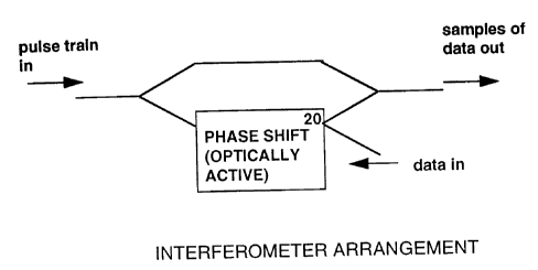
With reference to figure 3, which shows features of the invention,
an interferometer arrangement is shown including a phase shift
means 20. An optical pulse train is input at one side of the
S interferometer. Optical data is input at either side of the
interferometer, but to only one arm of the interferometer, so as to
alter the condition of interference of the interferometer. Thus the
output of the interferometer, constituted by a combination of the
optical signals in each arm, will depend on whether the optical signals
10 from the two arms combine with constructive interference or
destructive interference. The phase shift means 20 can be arranged
so that there is constructive interference when the data is high.
Alternatively, the arrangement can be made in inverting form, so that
there is constructive interference when the data is low. Alternatively,
15 the peak output, where there is constructive interference can be
arranged to coincide with the data beam at some point in-between
high and low levels.
Figure 4 shows input and output waveforms for the interferometer
20 of figure 3 operating as a sampler. In this case, a pulse train A is
input to both arms of the interferometer. Data in optical form is input
to one of the arms. The phase shift means 20, typically implemented
using a semiconductor optical amplifier, causes a phase shift in one
arm, which results in the output waveform C of figure 4. For high
25 levels of the data input signal, the pulse train is output in a similar
form to the pulse train input, owing to constructive interference.
Where the data level is low, owing to destructive interference, there is
little or no output. Accordingly, effectively the output can be seen as
the pulse train input modulated by the data, or it can be seen as
30 samples of the data, sampled by the input pulses.
In principle, various types of non-loop interferometer could be
used. The Mach-Zehnder type may be easiest to integrate and give
best results in terms of stability and ease of tuning. In principle, a
35 Michelson type interferometer could also be used.
CA 02222666 1997-11-26
1 ( )
Figure 3 shows the data being fed in the interferometer in the
opposite direction to the pulse train. This means the arrangement is
simpler because the data does not need to be filtered out of the
output. In principle the data could be fed into the interferometer in the
S same direction as the pulse train, in which case filtering would be
needed to remove the data signal from the output.
Three types of applications will be described for the arrangement
illustrated in figures 3 and 4. The first and second relate to optical
10 clock recovery. The third type relates to sampling a signal to
regenerate it optically without conversion to electrical form.
Clock Recovery Applications
Figure 5 shows an optical clock recovery arrangement 50
15 including a phase comparator 51, a clock generator 52, and a phase
loop filter 53. Conventionally, such an arrangement has been
produced for electrical signals, but it has been possible to achieve an
optical phase comparator only suitable for operation with optical
signals on which the data is coded in RZ form.
In the clock recovery arrangement of figure 5, the phase
comparator receives the optical data input signal and an optical clock
generated by the generator 52. Owing to the inbuilt stability of such
generators, the loop filter 53 can operate effectively with a bandwidth
25 much lower than that of the optical data signal. Accordingly, it is
feasible and less expensive to implement the clock phase control and
the clock generator in electrical form, and convert the electrical clock
to optical form before input to the phase comparator.
The optical phase comparator 51 is shown in schematic form in
figure 6. An interferometer 61 is provided for modulating the clock
with the optical data. The interferometer is biased to give a peak
output when the data is somewhere between high and low states, and
a reduced output at the high and low states. This enables the
interferometer to be responsive to data transitions, and thus
CA 02222666 1997-11-26
determine timing of pulses optically. The interferometer may be
arranged as shown in figure 3.
Figure 7A shows the typical waveforms when the interferometer
5 is used as a phase comparator, arranged to give peak output when
the data is halfway between high and low states. As a result, if the
phase of the clock drifts so as to take the clock pulses out of
synchronisation with the data, the output peaks shown in waveform C
of figure 7 would become changed in amplitude. Referring back to
10 figure 6, the output pulse train would be passed through integration
and low pass filtering functions 62. These would enable the phase
comparator output to be independent of data patterns since there will
be an averaging effect.
In practice this can be implemented by a PIN diode which would
output a low speed electrical signal, typically with a bandwidth of up
to hundreds of KiloHertz or a few MegaHertz, which can be fed back
as shown in figure 5 to the loop filter 53, which is an analog low pass
filter. The output of the filter is connected to the frequency control of
20 the oscillator. Thus a change in the amplitude of the pulses from the
interferometer could be detected as a change in the level of the
integrated filtered output of the PIN diode, which could cause the
frequency of the oscillator to adjust to compensate. Such phase
locked loop methods are well known and will not be described here in
25 more detail.
The output of the low frequency optical to electrical converter is
the convolution of the power in these pulses with its impulse
response. For conceptual simplicity, this can be thought of as
30 approximately the integral of the power in the pulses over a response
time of many thousands of pulses. Thus data with uneven amounts
of ones and zeroes can be handled, provided fluctuations in the
proportions of ones and zeroes don't have appreciable components
at frequencies below the threshold of the converter.
CA 02222666 1997-11-26
- 12-
The pulses output by the interferometer will be the strongest
when the clock input pulses coincide with the data being at the 50%
cross-over point, and will fall off with the cosine function as the data
approaches a 1 or O symbol.
s
In practice the input data will not have a square waveform but
may approach a raised cosine shape. In such a case the overall
response of the phase detector after integration by a low pass filter is
shown in figure 7B.
The phase locked loop is advantageously locked to the 0.5 level
of the phase detector output, and optical delay used to obtain the
desired clock to data phase. Locking to the 0.5 level of the detector
output gives the maximum control range (between O and 0.5 unit
15 intervals of relative phase), and uses the steepest slope on the
response curve, for strong feedback of phase error.
The clock pulses are preferably generated at the full bit-rate,
though sub-harmonics could be used.
Careful design and adjustment of the interferometer will enable
maximum output, inverting or otherwise, when the data signal is in
transition between logical states. In principle such transition could be
between multilevel logic states. For two level logic the interferometer
25 should give maximum output when the data signal has a power
amplitude of 50% of the eye. To achieve this, the relative phase shift
between the arms and the amount of phase shift which occurs in
response to the optical data input, can be adjusted. In practice,
amplitude saturation effects may also need to be considered. The
30 optical power in the data input may cause the gain of the optical shift
means to be altered or reduced. This also affects the condition of
interference, and will need to be accounted for when designing the
interferometer. An ideal response, ignoring gain effects, and for a
narrow clock pulse, much narrower than the bit period, is proportional
35 to the following equation:
CA 02222666 1997-11-26
cos(7t signal(nT+~))+1
where ~ is the phase of the clock pulse,
T is the bit period,
n is an integer,
and signal is the average power of the data, weighed over a clock
pulse,
centred at that time.
In this way, a phase comparator can be implemented which
15 enables the clock to be recovered independently of the type of coding
used for the data. In particular, it can operate on NRZ data, as used
in most high bit rate optical transmission systems.
Figure 8 illustrates the second optical clock recovery
20 arrangement 70, comprising a non-linear function operating on the
optical data, 71, followed by an optical narrow band filter 72 to extract
the clock frequency. The use of a non-linear function enables the
clock to be recovered from data such as NRZ data for which there is
little energy at the clock frequency. The non-linear function creates a
25 response at the clock frequency.
Figure 9 shows how the non-linear function 71 can be
implemented by an interferometer 80, arranged as in figure 3.
Instead of an input optical pulse train, because there is no separately
30 generated clock, continuous wave light is input. This is modulated by
the optical data, and the interferometer is biased to give a peak
output at data transitions, as described above in relation to figure 7.
If an optical pulse is output for each data transition, by the non-linear
function 71, the optical narrow band filter 72 shown in figure 8 can be
35 used to remove all but the clock frequency. Preferably the optical
narrow band filter is implemented by a means of a mode-locked laser,
although alternative implementations are conceivable.
CA 02222666 1997-ll-26
-14-
For systems where there are problems such as level variations,
or data patterning, that create excessive jitter, then the arrangement
of figure 10 can be used. The difference between outputs of two
5 samplers 91, 92, operating as phase comparators, are subtracted to
cancel common mode effects. A delay element 93 is provided to
delay the clock input of one of the phase comparators. The delay can
be arranged to be such that there is a minimal response from one of
the comparators when the other is giving a peak output. Thus the
10 outputs of the samplers 91, 92, are integrated and filtered by optical
to electrical converters 94 and 95. A subtractor 96 and low pass filter
97 can be used to derive an oscillator tuning signal from which
common mode effects have been cancelled out.
Optical Regeneration and Other Applications of Optical
Sampling
The optical clock recovery circuits discussed above can be used
in receivers or regenerators. They can be used in conjunction with
electrical signal reshaping and retiming, or used with optical retiming
20 and reshaping functions, to create an all optical regenerator, as
shown in figure 11. Sampler 100 is fed by the output of the optical
clock recovery function 101. A similar arrangement may occur at a
receiver, where the optical sampler 100 is used for retiming and
reshaping the optical data prior to conversion to electrical form, and
25 subsequent processing such as demultiplexing.
Figure 12 shows the optical regenerator of figure 11 in more
detail. The sampler 100 comprises an interferometer, biased to give
maximum output when the data input is in a given logical state. The
30 optical recovery circuit 101 also comprises an interferometer, this
time biased to produce a peak output on data transitions, to enable it
to function as a phase comparator. A semiconductor optical amplifier
102 acts as the optically active element for changing the interference
condition of the interferometer, according to the data signal fed into
35 the same arm of the interferometer. Phase shift means 103 is
provided for biasing the interferometer to achieve the desired
CA 02222666 1997-11-26
- 15-
function. A low pass filter 104 and optical clock 105 complete the
phase locked loop, to lock the optical clock to the transitions in the
data.
In the sampler 100, a semiconductor optical amplifier (SOA) is
again provided to alter the interference condition according to the
data signal, and phase shift means 107 is provided to bias the
interferometer to achieve the sampling function.
In this way, an all optical regenerator can be achieved capable of
handling NRZ data and capable of being integrated for cost effective
regeneration, particularly suitable for higher bit rate transmission
systems where electrical regeneration becomes more difficult and
expensive.
Figure 13 and 14 show applications of the optical sampler as
illustrated in figure 12 or in figure 3, in multiplexer arrangements.
Figure 13 shows a multiplexer arrangement in which multiplexing
is carried out by optical or electrical multiplex means 110, and then an
optical sampler 111 is provided to retime and reshape the combined
signal, for onward transmission. Synchronisation is provided by
clocks 112. Two clocks could be provided to the multiplexer 110 to
switch the two incoming data streams appropriately to enable time
division multiplexing. This could be on the basis of a bit interleave
scheme, though other well known schemes are conceivable.
Although only two data inputs are shown, obviously there could be
more.
An alternative multiplexer arrangement using the optical sampler
described above, is shown in figure 14. An optical sampler 111 is
provided for each of the optical data inputs to be multiplexed.
Separate clocks are provided for each sampler so as to sample each
optical data input at a different time interval. The mutually out of
phase output samples can then be combined optically to produce a
single multiplexed optical data output stream.
CA 02222666 1997-11-26
Figures 15 and 16 show corresponding demultiplexing
arrangements using the optical sampler described above. In figure
15 the sampler 111 is used to retime and reshape the incoming
5 optical data stream. This enables the optical or electrical
demultiplexer 120 to be of lower performance specification, since it is
fed with a clean optical signal with little jitter.
Figure 16 shows an alternative arrangement, in which multiple
10 optical samplers 111 are fed with the same input data stream.
Separate clocks are provided for each sampler so that samples are
taken at different times by different samplers. This enables the time
division multiplexed data to be separated out.
In principle, the demultiplexer arrangements of figures 15 and 16
could be used to decode multilevel logic signals. Different samplers
could be biased individually so as to give a maximum output for
different amplitude levels.
Interferometer Operation and Arrangements
As an alternative to the interferometer arrangement shown in
figure 3, figure 17 shows an arrangement in which the optically active
element, the optical amplifier is provided in both arms of the
interferometer. This makes it easier to balance the interferometer. In
principle, the interference condition of the interferometer, and
therefore the response at the output, is dependent on the amplitude
of the modulation of the optical waveform, and on the phase of the
optical waveform in each arm, ignoring polarisation effects. The
optical amplifiers 130 and 131 in figure 17 can alter the interference
condition. When data is input to the arm containing optical amplifier
131, the interference condition will be changed because the optical
amplifier has an amplitude to optical phase conversion effect. Ideally,
the pulses input to both arms, are sufficiently short and have
sufficiently low energy that the SOA does not react much to the
pulses. However, the SOA should have a sufficiently rapid response
time to react to the data waveform. The pulses input to both arms of
CA 02222666 1997-11-26
the interferometer can therefore be very narrow, as there is no limit
imposed by the speed of the response of the SOAs. Furthermore, it
is relatively easy to generate very narrow light pulses, on the order of
several picoseconds or less.
s
Construction of an integrated Mach-Zehnder interferometer for
use with high bit rates and with good performance characteristics is
described in IEEE Photonics Technology, Volume 8, September 1996
"Ten Gbs Wavelength Conversion With Integrated Multiquantum-
10 Well-Based Three-Port Mach-Zehnder Interferometer" by Idler et al.
The structure is grown by low pressure metal organic vapour phase
epitaxy. The device described can be used either for outputting
inverted or non-inverted data, with respect to the signal input data.
Although it is described for the purpose of wavelength conversion,
15 based on inputting a continuous wave into both arms of the
interferometer, such a device could be used for the application as
described above.
Figure 18 shows an alternative arrangement in which a
20 continuous wave bias is fed in in addition to the input pulses. This
enables the operating point of the amplifiers to be set. A filter 140
would be required to remove the continuous wave from the output. In
this figure and in figure 17, an output path at the top right is shown,
which is unused, and provided only for balancing the arrangement.
Figure 19 shows another interferometer arrangement in which
one of the optical amplifiers is replaced with an electrically controlled
phase shifter. An example of such a phase shifter is described in
Photonics Technology Letters, June 1990, pages 404 to 406, and
30 Photonics Technology Letters, August 1996, pages 1018 to 1020
(Rolland et al). The gain/loss of the arm containing the phase shifter
can be adjusted to match that in the arm containing the SOA. The
phase shifter can be used to set the desired condition of interference,
to enable peak output for the data input logic state being high, or low,
35 or somewhere in between, as desired.
CA 02222666 1997-11-26
One advantage of using such an optically passive device is that
less ASE (amplified spontaneous emission) noise is generated.
Furthermore, by using a phase shift device with little or no gain
variation, the interference condition can be controlled more easily,
S since there is independent control of gain and phase differences
between the two arms.
The electrically controlled phase shifter need only operate at low
frequencies, eg below 1 Megahertz, when only used for tuning. If a
10 high frequency phase shifter were to be provided, then combined
optical and electrical data inputs could be handled.
Figure 20 shows another interferometer arrangement. If the
phase shifter 160 is placed in the same arm as the SOA 161, the
15 other arm becomes a simple transmission line. This has the
advantage of better balance in the losses between the two arms. The
phase shift will tend to attenuate the signal. The SOA can
compensate for this by amplifying the signal. Electrically tuned
attenuators could also be added to either arm, to balance the power
20 levels. Other elements which have an optical phase shift in response
to an optical power level could be used in place of the SOA. Other
interferometer configuration such as a Michelson arrangement could
be used. The entire device could be integrated for a low cost high
volume production, using methods such as those discussed by
25 Rolland et al.
All the arrangements discussed could be used either in the
sampler or the phase detector or the non-linear response applications
of the interferometer. A two stage interferometer arrangement will
30 now be discussed with reference to figure 21, which is particularly
applicable to the sampler.
The Two Stage Interferometer Arrangement
Figure 21 shows an arrangement which would be suitable for
35 replacing the single interferometer of the sampler in figure 12. The
first stage comprises an interferometer having SOAs 170 and 171.
CA 02222666 1997-11-26
- 19-
Continuous wave light is fed into both arms, and data is fed into one
arm. The gain in the first stage can be arranged to be sufficient to
drive the first stage output to its limit for one level of input data (high
or low depending on whether the stage is to be inverting or not). This
5 effectively makes gradual data transitions steeper, and flattens one of
the logic states.
The second stage can be arranged to drive its output to its limit
for the other logic level. Thus the data can be reshaped optically. If
10 no retiming is required, but only reshaping, the second stage could be
fed with continuous wave light. Alternatively, the retiming could be
implemented by feeding the first stage with a pulse train.
Figure 22 shows the output power for the first stage versus input
15 power, where the first stage is an inverting stage. For a logical zero
data input, the power output is high, driving the output to its limit, and
thus flattening the logic level 1 of the output. The output of the first
stage should follow a response curve which is less steep than a 1/x
curve at low input powers, and is flatter than the 1/x curve at higher
20 input powers, but steeper at intermediate powers. Such a shape,
when used in two stages results in the overall response shown in
figure 23. For good sampling of data and to produce steep
transitions, the transition range should be as short as possible.
Furthermore, the transition range should be located so as to be
25 centred around the threshold between high and low logic states for
the input signal. If inverting devices are used, the transition can be
centred more easily since the inversion causes the second stage
response to balance the steepest portion of the first stage response,
rather than accentuate it.
In principle, a device with more than two stages could be
constructed. Furthermore, the stages could be in parallel rather than
in series. If in parallel, some sort of time division multiplexing for the
two logic states would be required. Furthermore, the stages could be
35 non-inverting, though for interferometers at least, the inverting
response is preferable. Optical devices other than interferometers
CA 02222666 1997-11-26
-20-
could be used if they have a non-linear response similar to that
shown in figure 22.
For good optical regeneration of data, a short transition range will
S determine how steep the transitions of the change in interference
condition of the second interferometer are. In turn, this can effect the
sampling process which takes place in the second stage. If the
second stage is fed by continuous wave light, the steepness of
transition in interference condition will determine the shape of the
10 output data transitions.
Figure 24 shows at waveform A the data input. The output of the
first inverting interferometer is shown in waveform B, which has
steeper transitions than waveform A. The pulse train of waveform C
15 is the other input to the second interferometer. Waveform D shows
how the interference condition of the second interferometer is
dependent on the output of the first interferometer.
The limiting action of the first interferometer would remove noise
20 from the signal for the period when the data input is in a high state.
However, noise at the low state of the data input, would remain on the
output of the first inverting interferometer. However, the interference
condition of the second interferometer, shown in waveform D, would
exhibit little noise on either the high level state or the low level state.
25 Furthermore, the transitions in waveform D would be even steeper
than those in waveform B, owing to the response of the type shown in
figure 22. This leaves a relatively wide Ueye'', for the sampling pulse
of the pulse train in waveform C. Accordingly, the output waveform E
in figure 24 will be relatively free of noise, and relatively immune to
30 jitter in the data input.
For devices or arrangements where there is a limited amount of
gain, and therefore only moderate limiting, the regeneration
performance may not be as good in terms of jitter immunity and noise
35 reduction, as can be achieved with electrical regeneration. For
example, if the gain is limited to a factor of 3, a signal at 10% above
CA 02222666 1997-11-26
the threshold between high and low, might be increased to 30%
above the threshold. If the threshold is set at 50% of the maximum
signal, then the output would be up to 80% of the maximum, and
therefore the limiting action would be only partial. Nevertheless, it
S would clearly be beneficial, even without complete limiting up to 100%
of the signal range.
If the response curves for the two individual stages are not
identical, then the overall response shape can be altered by altering
10 the relative gains of the two stages. This adds an extra degree of
freedom. In designing the device, the amplification characteristics of
the optical amplifiers in the interferometers can be varied. The
relative powers of the three inputs, the data input, the continuous
wave input, and the pulse train input, can be varied. Furthermore, the
15 coupling between the two stages can be varied. In this way, the two
stage device offers more flexibility for tailoring the response to the
needs of the particular application.
There are a number of applications where such partial optical
20 regeneration would be useful. Firstly, inside an optical amplifier, eg a
bi-directional optical amplifier, having multiple stages, improved
performance could be achieved if the output of a first stage of
amplification was subject to such partial optical regeneration, before
passing through a filter and into a second stage of amplification.
25 Noise and jitter could be reduced.
Secondly, inside an optical switch, it could be useful to have
partial optical regeneration to avoid accumulation of degradations.
Finally, partial optical regeneration would be useful if applied
between WDM subnetworks, for purposes of at least partial isolation,
so that each subnetwork could be operated and specified
independently of the degradations occurring in neighbouring
networks.
CA 02222666 1997-11-26
-22-
Other variations will be apparent to a person skilled in the art,
falling within the scope of the claims.