Note: Descriptions are shown in the official language in which they were submitted.
CA 02222847 1997-11-28
ION MOBILITY SPECTRONETER
BAC~GROUND AND SU~ RY OF THE INVENTION
This application claims the priority of German patent
document 196 50 612.3, the disclosure of which is expressly
incorporated by reference herein.
The invention relates to an ion mobility spectrometer with
an ion gate, a drift chamber, and an ion collector.
An ion mobility spectrometer of this generic type is
described for example in European patent document EP 0 046 699
and in U.S. Patent 4,390,784. It is essentially based on the
fact that ions migrate to the ion collector in the drift chamber
under the influence of an electrostatic field. The drift time
is different for different ions and is determined by their
mobility. The known ion mobility spectrometer has a drift
chamber cross section of several centimeters and drift distances
up to 40 cm. The dimensions and high price of such devices limit
the type and number of applications that lend themselves to this
measurement method.
Attempts therefore have been made to miniaturize ion mobility
spectrometers (International Journal of Environmental Analytical
Chemistry, 1993, Volume 52, pages 189-193). Implementation of
the concept described therein however has proven to be difficult
or impossible, since the requirements for the individual
components can be met only with difficulty if at all. No mention
CA 02222847 1997-11-28
is made in the above article of the technical implementation of
a miniaturized ion gate.
Hence, the object of the present invention is to provide an
ion mobility spectrometer that can be miniaturized, and which can
be manufactured using conventional methods, especially those
known from semiconductor manufacturing.
Another object of the invention is to provide an ion
mobility spectrometer which is small and less expensive to
manufacture than known prior art devices.
These and other objects and advantages are achieved by an
ion mobility spectrometer (IMS) according to the invention, in
which the essential parts, namely the ion gate, the drift
chamber, and the ion collector, consist of pieces that are
essentially slice or wafer shaped, which are either
anisotropically etchable or can be machined using micromechanical
methods, and are held together by clamps, adhesives, or other
assembly methods that are known of themselves . In the simplest
form, the drift chamber consists of t~o sliced pieces with a
through groove being etched or milled in one of them. The groove
is covered by the other smooth piece so that a drift channel is
produced. The drift channel is closed at one end by a grid-
shaped ion gate, which is similarly made from a sliced piece by
etching or milling, while the opposite end of the drift channel
is closed by the ion collector, which is likewise made from a
sliced piece that is electrically conducting on the inside.
CA 02222847 1997-11-28
In this manner, an IMS can be produced with a drift chamber
cross section of less than 1 cm and a length of approximately 4
cm; in other words dimensions that correspond to about 1/10 of
the previously conventional device measurements. The ionization
chamber, which directly abuts the ion gate, can also be made in
the same fashion.
Because of the small dimensions of the drift chamber, the
measurement pulses are nearly delta-shaped with proper control
of the ion gate, so that a detection limit for specific ions in
the ppm range can be set. The power draw of the device can
therefore be kept below 2 watts.
Because of its miniaturization, its low energy demand, and
its low cost, the IMS can be used for drug or dangerous substance
detection in the field, and can also be used for example as a
monitoring device on high-voltage switches, which are filled with
a protective gas (sulfur hexafluoride), whose concentration must
be constantly monitored. Thus, frequent changing of the
protective gas can therefore be eliminated.
Other objects, advantages and novel features of the present
invention will become apparent from the following detailed
description of the invention when considered in conjunction with
the accompanying drawings.
CA 02222847 1997-11-28
BRIEF DESCRIPTION OF THE DRAWINGS
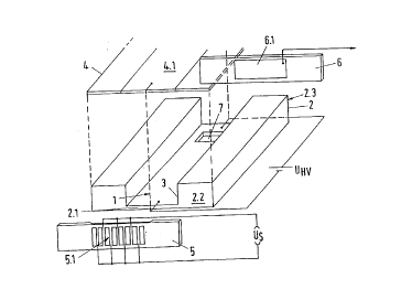
The single figure of the drawing shows an exploded view of
an embodiment of the invention, partially in schematic form.
DETAILED DESCRIPTION OF THE DRAWINGS
The Figure shows the structure of a drift chamber for an IMS
according to the invention. Drift channel 1 is formed
essentially by a silicon slice 2 about 1 mm thick and 40 mm long,
in which slice a groove 3 has been etched or milled in such
fashion that a layer with a thickness of approximately 20 ~m is
obtained that forms the lower side wall 2.1 of drift channel 1
of silicon slice 2. The upper side wall of drift channel 1 is
formed by a cover plate 4 made of silicon which is glued flush
on the remaining surfaces of slice 2. The front of drift chamber
l is closed by a silicon slice 5 into which a gas-permeable grid
5.1 is etched in the vicinity of the drift chamber, with the
individual grid rods being electrically conducting, by
metallization for example, and with e-ach rod being -connected
actively to the next grid rod but one. This silicon slice 5
forms the ion gate, and is glued to end 2.2 of-silicon disk 2.
The back of drift chamber 1 is sealed by a silicon slice 6
which is likewise electrically conducting in the vicinity of the
drift channel and serves as an ion collector. This silicon slice
6 is glued to end 2.3 of silicon disk 2.
--4--
CA 02222847 1997-11-28
In the bottom 2.1 of silicon slice 2, in the vicinity of ion
collector 6, an opening 7 is etched that serves as a throughput
opening for the drift gas.
To produce a drift field that is as disturbance-free and
homogeneous as possible, both the bottom 2.1 of the silicon slice
2 and the portion 4.1 of silicon slice 4 that forms the cover of
the drift chamber are provided with a high-ohmage resistance
layer. The latter layers preferably are applied to the outside
walls of the materials in order to avoid chemical influences on
the ions, caused by the drift gas. Instead of resistance layers
that have been applied, the silicon slices can also be doped in
order to acquire the electrical conductivity that they require
for developing a field in areas 2.1 and 4.1. The drift field is
then produced by an external voltage U~ of approximately 2000 V,
applied to the ends of the conducting layers of 2.1 and 4.1.
The drift gas can flow in drift chamber 1, depending on the
requirements, either from opening 7 at ion gate 4, through grid
rods 5.1, or in the opposite direction. The ions of the sample
to be measured are generated in an ionization chamber (not shown)
that can have essentially the same miniaturized design as the
drift chamber and is placed on the front of ion gate 5. Grid 5.1
of ion gate 5 is controlled by a voltage Us in known fashion.
That is, when a potential is applied between adjacent grid rods,
the ion gate is blocked; and when no potential is applied, the
ion gate is per~eable to the ions from the ionization chamber.
In the latter case, the ions are accelerated in the drift channel
CA 02222847 1997-11-28
by the field of voltage U~ toward ion collector 6, where they
strike collecting plate 6.1 and generate an electrical signal
there, which is evaluated in known fashion.
To create a uniform flow of the drift gas it is advantageous
for through opening 7 to have a cross section that corresponds
roughly to the cross section of drift channel 1 through which
flow occurs.
It is possible to achieve a larger drift channel cross
section; for example, by using in place of a plane cover plate
4, a part that is symmetrical with respect to silicon slice 2,
and has a groove with the same coverage. The silicon slices 5
and 6 of the ion gate and/or ion collector are then enlarged
accordingly, so that they cover drift channel 1, which is then
twice as high.
Instead of silicon, of course, other materials that are
either anisotropically etchable or can be machined by
micromechanical means, for example gallium arsenide, glass, and
the like, can be used for the components of the drift-chamber.
Although the invention has been described and illustrated
in detail, it is to be clearly understood that the same is by way
of illustration and example, and is not to be taken by way of
limitation. The spirit and scope of the present invention are
to be limited only by the terms of the appended claims.