Note: Descriptions are shown in the official language in which they were submitted.
CA 02223116 2001-07-17
CDMA CHIP SYNCHRONIZATION CIRCUIT
This invention relates to CDMA chip synchronization circuits which are
provided in CDMA receivers to perform synchronous detection with respect to
receiving
timing of radio frequency signals.
The CDMA chip synchronization circuit (wlhere'CDMA' stands for 'Code
Division Multiple Access') is provided in the receiver of the mobile
communications
system, particularly in the receiver of the automobile phone and portable
phone system
(which will be simply called "cellular system") using the DS-CDMA method
(where 'DS-
CDMA' stands for 'Direct Spread CDMA'). In other words, the CDMA chip
synchronization circuit is used to detect the receiving timing at the base
station receiver.
Examples of the spread spectrum communications are disclosed by the
papers of Japanese Patent Laid-Open Publications Nos. 4-347944 and 6-284111
both
of which relate to the synchronization device for the spread spectrum
communications
equipment as well as Japanese Patent Publication No. 2-39139 which relates to
the
receiver of the spread spectrum communications method, for example. In
addition,
other information regarding the disclosure of the spread spectrum
communications is
disclosed in, for example, Chapter 6 and Chapter 7 of the paper entitled
"TIAIEIA
INTERIM STANDARD (TIAIEIAIIS-95-A) Mobile Station-Base Station Compatibility
Standard for Dual-Mode Wideband Spread Spectrum Cellular System PN-3421 (to be
published as IS-95-A)" which is published by the Telecommunication. Industry
Association (TIA) on May of 1994 as well as Figure 3.1, Figure 3.2, Figure 3.6
and
pages 39-66 of Chapter 3 of the paper entitled "Principles of Spread Spectrum
Communication" which is written by Dr. Andrew J. Viterbi and published in May
of 1995
by Addison-Wesley Publishing Company.
1
CA 02223116 2001-07-17
Among the conventional mobile communications systems, the so-called
North American standard method (i.e. TIA IS95) is known as the digital
cellular system
using the CDMA method. In the standard specification of TIA/EIA/IS-95-A,
Chapter 6
describes operations required for the mobile station, while Chapter 7
describes
operations required for the base station. However, the above standard
specification
merely provides standardization for the radio interface. For this reason, the
standard
specification describes the modulation method and signal formats but fails to
describe
the concrete receiving method.
The forward link of IS-95-A (which is used to pertorm transmission from
the base station to the mobile station) performs transmission of pilot
channels (PLCH)
in addition to transmission of traffic channels (TCH). Herein, the traffic
channels are
provided for multiple users subjected to modulation by information, whilst the
pilot
channels are not subjected to modulation by information. Further, the
transmission of
the pilot channels is performed using relatively intense electric power. Using
the pilot
channels, the mobile station is capable of determining the optimum receiving
timing.
So, the mobile station does not suffer as much from a problem that the
receiving timing
should be determined under low EbINo (where 'Eb' denotes energy of receiving
signals
per 1 bit of information; and 'No' denotes electric power density of noise and
interference signal per 1 Hz). However, transmission of the pilot channels
using the
intense electric power results in reduction of a number of traffic channels
which are used
for actual transmission of information. This causes another problem that a
number of
users per one base station should be reduced.
On the other hand, no common pilot chaninels exist in the reverse link of
IS-95-A (which is used to perform transmission from the mobile station to the
base
station). So, the reverse link employs the modulation method corresponding to
the
2
CA 02223116 2001-07-17
64-ary.orthogonal code modulation combined with the quadruple direct spread.
Using
the 64-ary orthogonal codes, as compared with the BPSK and QPSK (where 'BPSK'
stands for 'Binary Phase-Shift Keying' and 'QPSK' standls for 'Quaternary
PSK'), it is
possible to provide a variety of advantages.
It is possible to increase electric power per one symbol and it is possible
to reduce deterioration for synchronous detection even if asynchronous
detection is
employed.
However, the above has problems relatinc,~ to the receiving method.
Main elements of the IS-95-A are determined such that the chip rate is
set at 1:2288 Mcps, the bit rate is at 9.6 kbps and the spread rate of the
direct spread
is at 128. According to the above, the chip rate is relatively low speed
(because of the
narrow-band CDMA), wherein compared with instantaneous variations of the
propagation delay, wherein the chip period is relatively long. For this
reason, the
amount of deterioration in receiving characteristics is small even if
characteristics of the
receiving timing detecting circuit are somewhat loose. However, to perform
high-speed
data communications with respect to voices and other information, it is
necessary to
increase the bit rate and chip rate by a certain factor of multiplication
which ranges
between 5 and 10; in other words, it is necessary to provide the wide band
CDMA. In
that case, other problems occur which the IS-95-A cannot expect. In the case
of the
chip rate of 10 Mpcs, for example, if the propagation path differs by 30 m,
the receiving
timing deviates from the original timing with respect to one chip only. So, it
is not
possible to receive signals with the original timing. In addition, a plurality
of multipaths
overlap with each other within a range of delay times corresponding to
multiple chips.
In that case, there is a problem that positions of peaks cannot be clearly
defined.
3
CA 02223116 2001-07-17
A conventional example of the receiving timing detection method (or chip
synchronization method) is taught by the paper entitled "Principles of Spread
Spectrum
Communication" which is written by Dr. Andrew J. Viterbi and published in May
of 1995
by Addison-Wesley Publishing Company. The operation t~o capture the timing of
signals
which are spread by spread codes corresponding to pseudo-random codes is
performed
in two stages of processing. That is, the method performs initial synchronous
capture
(or initial synchronous search) and synchronous tracking.
The method of the initial synchronous search is explained in the fourth
paragraph of Chapter 3 of the above paper. According to this method, until the
correlation electric power exceeds a certain threshold value, the search is
performed
in a serial manner with shifting the receiving timing by a half chip space.
The synchronous tracking corresponds to tlhe method of so-called "early-
late gate" or "delay lock loop (DLL)". This method calculates first
correlation electric
power corresponding to the early timing which is earlier than the reference
timing by the
delay time ~t for the receiving and second correlation electric power
corresponding to
the late timing which is later by fit. Then, the method performs the timing
adjustment
in such a way that a difference between the first electric power and second
electric
power becomes zero.
Meanwhile, Japanese Patent Laid-Open Publication No. 4-347944
discloses some improvements to the method of the iniitial synchronous search
and
synchronous tracking. Particularly, the paper discloses the method regarding
the
commonality of circuits as well as the method to add tracking function to the
multipath
propagation path. However, the basic operation of the above method is
identical to that
of the aforementioned paper written by Dr. Andrew J. Viterbi. In addition,
this method
is not capable of solving the aforementioned problems in the wide band CDMA.
4
CA 02223116 2001-07-17
Japanese Patent Publication No. 2-39139 describes a method to search
a new path wherein operation of the sliding correlator is not made only in the
initial
synchronous search but is made normally. Similar de;>cription is found in
Japanese
Patent Laid-Open Publication No. 6-284111. According to the above method which
is
designed to perform searching of new paths normally, it is possible to shorten
the
instantaneous break time in communications. However, it cannot be said that
the
method is capable of detecting peak positions accurately with a short time.
In short, the mobile communications system using the CDMA method
performs receiving of so-called multipath signals, wherein the system should
perform
matching of timing with respect to each of signals. Herein, the multipath
signals are
transmitted to the system via multiple propagation paths which differ from
each other
in propagation time due to the reflection by buildings and mountains, for
example. To
achieve effective usage of frequencies in communications, each channel should
have
a capability of receiving signals under the very low EblNo environment.
Particularly, in case of the wide band CDIVIA method whose chip rate is
10 Mcps or so, the receiving timing is shifted by one chip when the
propagation distance
changes by 30 m. Such a shift makes the receiving operation impossible. A
difference
of propagation delay corresponding to a difference of propagation distance of
30 m or
so easily occurs when a small variation occurs in the propagation path even if
the
distance between the base station and mobile station is unchanged. In other
words,
frequently there occurs a phenomenon that the receiving is performed with
respect to
the multipaths which overlap with each other in a range of multiple chips, and
variations
simultaneously occur with respect to receiving paths (i.e., emergence and
vanishing of
new paths).
5
CA 02223116 2001-07-17
Conventionally, the DLL technology is used for the synchronous tracking
of the receiving timing. This technology is effective under prescribed
conditions that
each multipath has a separate peak and the propagation delay time continuously
and
gradually changes. In contrast, the wide band CDMA works under the condition
where
the receiving is performed with respect to the multipaths iin an overlap
manner and the
delay time discontinuously changes. So, the wide band C;DMA suffers from a
problem
due to its inability to perform the tracking
It is an object of the invention to provide a CDMA chip synchronization
circuit for the mobile communications system employing iihe wide band CDMA
method
so that adjustment of multiple receiving timing, particularly synchronous
tracking, can
be performed under a low EbINo environment.
As a result of this invention it is possible to improve receiving quality of
a wide band CDMA receiver and it is possible to perform high speed data
transmission.
A CDMA chip synchronization circuit of this invention is provided for a mobile
communications system employing a wide band CDMA method, especially direct
spread
code division multiple access (DS-CDMA) method.
As a result of this invention, it is possible 1:o improve receiving quality of
a wide band CDMA receiver; and it is possible to perform high-speed data
transmission.
A CDMA chip synchronization circuit of tlhis invention is provided for a
mobile communications system employing a wide band CDMA method, especially
direct spread code division multiple access (DS-CDMA) method.
In the CDMA chip synchronization circuit; a radio receiver converts radio
frequency signals to digital base band signals, whilst a search section
detects receiving
timing with respect to multipath components contained in the digital base band
signals.
The detected receiving timing is used as a center positicm for receiving on a
time axis.
6
CA 02223116 2001-07-17
The radio receiver is connected with multipath receivers, each of which
contains a
number of correlators which produce correlation values between the multipath
components and dc-spreading codes which are delayed by different delay times
respectively. Herein, the correlators correspond to prescribed intervals of
time which
deviate from the center position for the receiving on the time axis.
Correlator outputs
are temporarily stored in a memory. Then, the multipath receiver selects a
correlator
output having a best receiving quality from among the correlator outputs by
every
prescribed interval of time corresponding to a pilot period, so synchronous
detection is
performed using the selected correlator output. Outputs of the multipath
receivers are
combined at a maximum ratio, so that receiving data are produced.
Thus, the CDMA chip synchronization circuit of this invention has a
capability to certainly perform detection of mulitpath receiving timing,
particularly
synchronous tracking, under a low EbJNo environment where multipaths are
received
in an overlap manner.
These and other objects of the subject invention will become more fully
apparent as the following description is read in light of the: attached
drawings wherein:
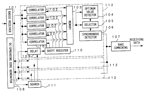
Figure 1 is a block diagram showing a CDNIA chip synchronization circuit
in accordance with an embodiment of the invention;
. Figures 2A and 2B are graphs showing relationships between delay time
and receiving level with respect to models of propagation characteristics of
the wide
band CDMA method which the invention employs; and
Figure 3 shows an example of a signal format.
Now, a preferred embodiment of the invention will be described with
reference to Figure 1 to Figure 3.
7
CA 02223116 2001-07-17
Figure 1 is a block diagram showing a CDMA chip synchronization circuit
in accordance with an embodiment of the invention. In Figure 1, a radio
receiver 101
receives radio frequency signals and converts them to digital base band
signals. A
plurality of multipath receivers, each designated by a same numeral of "112",
are
provided to perform decoding processes with respect to multipath components
contained in the digital base band signals. Herein, each multipath receiver
112
performs a decoding process with respect to each multipath component. Then,
the
decoded multipath components are supplied to a RAKE combining section 107
wherein
they are combined at a maximum ratio. So, the RAKE connbining section 107
produces
receiving data. A dc-spreading code generator 108 generates dc-spreading codes
which reversely spread spectrum. A search section 111 nneasures the receiving
timing
with respect to the multipath components.
Next, the multipath receiver 112 is configured as follows:
A delay section 109 delays the dc-spreading codes to coincide with the
receiving timing which the search section 111 detects. A shift register 110
further
delays the delayed dc-spreading codes, output from the delay section 109, by
different
delay times. Herein, the shift register section 110 has multiple output
terminals
corresponding to different delay times which differ from each other by a
constant delay
which corresponds to'/4 chip, for example. A plurality of correlators, each
designated
by the same numeral of "102", produces correlation values between the digital
base
band signals and outputs of the shift register 110. Thus, the correlators 102
as a whole
perform operation of "dc-spreading" with respect to receiving signals. A
memory 103
temporarily stores (or accumulates) outputs of the correlators 102. An optimum
value
detector 104 and a selector 105 cooperate to intermittently perform reading
operations
on the memory 103 by certain intervals of time, thus selecting a correlator
output which
8
CA 02223116 2001-07-17
has a best receiving quality. Using the selected correlator output, a
synchronous
detector 106 performs synchronous detection.
Under a real propagation environment, a number of the multipath
receivers 112 is determined based on a trade-off relationship established
between a
maximum number in effective numbers of the multipaths and the hardware scale.
Normally, in the case of a city environment, it, is sufficient to provide four
multipath
receivers per one radio signal receiver (which corresponds to one antenna).
One
multipath receiver 112 contains five correlators 102 which produce correlation
values
with respect to five timings. Herein, the timing designatecl by the search
section 111 is
used as the center of the five timings. So, there are provided five timings
which are
represented by 0 (i.e., center), t'/4 chip and t'/2 chip re;>pectively.
In the above case, the memory 103 should have a capability to store five
correlator outputs. Namely, the memory 103 stores one slot, which is
partitioned by a
pilot symbol, with respect to each correlator output.
The mobile station performs transmission of reverse signals which are
placed in frame synchronization with forward signals which are transmitted
from the
base station to the mobile station. So, the search section 111 of the base
station has
a capability to perform path search within a prescribed range of propagation
delays in
accordance with a radius of a service area which covers one base station. The
method
of the path search for the base station is shown in Japanese Unexamined Patent
Publication No. Hei 10-32523 published February 3, 1998.
Next, processing of the optimum value deflector 104 will be explained in
conjunction with Figures 2A and 2B.
9
CA 02223116 2001-07-17
Figures 2A and 2B are graphs showing relationships between delay time
and receiving level with respect to models of propagation characteristics
(i.e., delay
profiles) of the wide band CDMA method which the invention employs.
The above graphs are made in connection with two independent groups
of multipaths, each group of which contains three paths which overlap with
each other
and which deviate from each other by'/2 chip.
In the case of the graph of Figure 2A, a first group of three paths are all
received with a same phase. Thus, the three paths are enhanced in receiving
level so
that a peak emerges at the center of the three paths on a time axis. As for a
second
group of three paths, a center path is received with a phase which is inverse
to phases
of other paths. Therefore, the three paths are cancelledl with each other in
receiving
level, so that the receiving level of the center path should become very
small. For this
reason, two sub-peaks emerge in the receiving level regarding the second group
of
paths.
In the case of the graph of Figure 2B, as for the first group of three paths,
only a last path is received with an inverse phase, so that a position of a
peak is shifted
in a backward direction from a center position by'/Z chip on a time axis. In
addition, a
small sub-peak emerges at a position which is'h chip after the center
position. As for
a second group of three paths, two paths other than a first path are received
with
inverse phases, so a position of a peak delays from a center position by'h
chip.
As described above, in the case where the system (e.g. station) receives
multiple multipaths in an overlap manner with small shifts of phases, even if
the paths
do not change in receiving timing and receiving level, a peak in an overall
receiving level
fluctuates in position and level.
The receiver applicable to this invention is designed as follows:
CA 02223116 2001-07-17
A search section detects positions with rE~spect to groups of paths, to
which multipath receivers are assigned respectively. Herein, each multipath
receiver
uses the timing that the search section detects as a center position for
receiving on a
time axis. So, the multipath receiver has multiple correlators which perform
dc-
spreading on receiving signals with respect to both forward and backward
directions
from the center position on the time axis. That is, the correlators are
provided to cope
with delays of the timing which correspond to t'/2 chip .and t'/4 chip from
the center
position. Then, the multipath receiverselects a correlator .output having a
best receiving
quality from among correlator outputs which are provided with certain
intervals of time.
So, the multipath receiver performs decoding of the selected correlator
output.
In case of the second group of paths shown in Figure 2A, the sub.-peaks
emerge at different timings which separate from each other by 1 chip or more,
it can be
presumed that noise contained in one sub-peak is independent from noise
contained
in another sub-peak. In case of the first group of paths shown in Figure 2B, a
relatively
large sub-peak emerges at the timing apart from the peak by 1 chip or more.
The present embodiment can be modified to cope with the above cases.
That is, the present embodiment can be modified in such a way that two
correlator
outputs corresponding to two peaks (or sub-peaks) are extracted and combined.
Figure 3 shows an example of a signal format applicable to this invention.
Herein, 'PL' designates a pilot symbol.
As shown in Figure 3, a "known" pilot signal is periodically inserted into
transmission of data by a constant period (i:e., pilot period which is set at
0.625 ms, for
example) which is shorter than a fading period. In that case, the above pilot
signal can
be used as a reference signal for synchronous detection, details of which will
be
described below.
11
CA 02223116 2001-07-17
The pilot period is used as a partition of transmission. So, multiple
correlator outputs are stored in the memory. The system measures receiving
quality of
signals contained in the pilot period with respect to each of the correlators.
Then, the
system selects a correlator output having a highest receiving quality. Or, if
a sub-peak
is detected at a position which sufficiently is separated from the timing
(i.e., peak
position) of the correlator having the highest receiving quality and which is
considered
to be independent from noise, the system extracts a correlator output
corresponding
to the sub-peak from the memory. Thus, the synchronous detection is performed
by
using the pilot signal as the reference signal representing carrier phase.
Incidentally, it is possible to employ a variety of methods for
determination of the receiving quality for each of the correlator outputs, as
follows:
(1 ) Determination is made based on the receiving level of the pilot signal.
(2) If the pilot signal is constructed by multiple symbols, determination is
made based on a ratio between a square of an average value (i.e., presumed
value of
signal power) and a variance (i.e., presumed value of noise power).
(3) Determination is made by measuring receiving levels with respect to
the pilot signal portion as well as the data portion.
(4) Temporary decision is made with respect to the data portion.
Reverse. modulation is effected on the receiving data on the basis of the
result of the
temporary decision, so phases of all data are made uniform with the carrier
phase.
Then, a determination is made based on a ratio between a square of an average
value
(i.e., presumed value of signal power) and a variance (i.e., presumed value of
noise
power).
Finally, this invention is capable of demonstrating a variety of effects,
which the conventional technology cannot provide, as follows:
12
CA 02223116 2001-07-17
(1) It is possible to perform fine adjustment for the optimum receiving
timing by a certain period, e.g., a pilot period for insertion of a pilot
signal into
transmission of data. So, even in the wide band nDMA under a propagation
environment where the receiver performs receiving with respect to multipaths
which
overlap with each other, it is possible to perform synchronous tracking to
follow
variations of peaks in receiving level. Namely, it is possible to perform
receiving in a
stable manner.
(2) It is possible to loosen a detection pn~cision of the search section.
For this reason, it is possible to reduce a time for averaging at a search
mode.
Therefore, it is possible to perform fast detection of a nE:w path even if a
propagation
path rapidly changes.
As this invention may be embodied in several forms without departing
from the spirit of essential characteristics thereof, the present embodiment
is therefore
illustrative and not restrictive, since the scope of the: invention is defined
by the
appended claims rather than by the description preceding them, and all changes
that
fall within metes and bounds of the claims, or equivalence of such metes and
bounds
are therefore intended to be embraced by the claims.
13