Note: Descriptions are shown in the official language in which they were submitted.
CA 02223227 1997-12-02
,
TITLE OF THE INVENTION
POWER CONVERTER
6 BACKGROUND OF THE INVENTION
1. Field of the Invention
The present invention relates to power converters and
more particularly, high voltage, large capacity power
converters which connect in series multiple self-turn-off-
semiconductor devices.
2. Description of the Related Art
In recent years, power converters which can supply high
voltages and large currents have been desired. In particular,
the ability to supply 2000 ~ 3000A or more at 100 ~ 500KV is
required by DC transmission and the like.
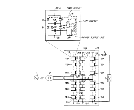
Fig. 1 is a block diagram of the overall composition of
a prior art power converter and of a switch unit. Fig. 2 is
a block diagram of the control signal supply circuits for the
gate circuits which compose the power converter in Fig. 1.
In Fig. 1, AC power source 1 is connected to converter
3 via transformer 2.
This converter 3 provides self-turn-off-semiconductor
devices which are bridge-connected. The following is the
description ofthe case when the composition uses gate turn-off
CA 02223227 1997-12-02
thyristors (hereafter, referred to simply as "GTO") as one
example. The DC current which is the output of this converter
is smoothed via DC reactor 4 and supplied to DC circuit (load)
5.
6 Thepartstowhichsymbols 61and71areassignedareGTOs.
The parts to which symbols 81 and 91 are assigned are diodes.
When GTOs 61 and 71 turn off, the current which was flowing in
GTO 61 and 71 is led to capacitor 101. Capacitor 101 operates
as a so-called snubber capacitor which restricts the forward
voltage rising rates dv/dt of GTOs 61 and 71 to the permitted
values for the GTO elements or less when GTOs 61 and 71 turn
off. The charge accumulated in capacitor 101 is regenerated
to AC power source 1 or DC circuit 5 via converter 3 when GTOs
61 and 71 turn on. The above GTOs 61 and 71, diodes 81 and 91
and capacitor 101 compose U-phase switch unit 111.
U-phase switch units 112 ~ lln are composed in the same
way.
Also, V-phaseswitchunits121~12n, W-phaseswitchunits
131 ~ 13n, X-phase switch units 141 ~ 14n, Y-phase switch units
151 ~ 15n and Z-phase switch units 161 ~ 16n are composed in
the same way.
Converter 3 is composed by bridge-connecting arms 11 ~
16whichareformedfromtheaboveU-phaseswitchunits~Z-phase
switch units.
In Fig. 2, the composition of the arms is illustrated,
taking U-phase arm 11 as an example.
CA 02223227 1997-12-02
The parts designated by symbols 191 ~ l9n and 201 ~ 20n
are gate circuits which output gate signals 171 ~ 17n and 181
~ 18n in order to turn on or turn off the respective GTOs 61
~ 6n and 71 ~ 7n.
The control signals which control the turning on and off
of each gate circuit 191 ~ l9n and 201 ~ 20n are transmitted
from control system 25 via control signal lines 231 ~ 23n and
241 ~ 24n. Generally, optical cables are used for control
signal lines 231 ~ 23n and 241 ~ 24n, and optical insulation
is performed between control system 25 and gate circuits 191
~ l9n and 201 ~ 20n.
The power for driving gate circuits 191 ~ l9n and 201 ~
20n is obtained from power supply unit 27. Power supply unit
27 is connected to AC power source 26 which is obtained
externally such as utility lines, and outputs a stabilised AC
voltage with little voltage fluctuation. Insulation between
power supply unit 27 and gate circuits 191 ~ l9n and 201 ~ 20n
is performed by transformers 211 ~ 21n and 221 ~ 22n.
V-phase arm 12, W-phase arm 13, X-phase arm 14, Y-phase
arm 15 and Z-phase arm 16 are composed in the same way.
The followingis adescriptionoftheoperationofaprior
art power converter, referring to Fig. 1 and Fig. 2.
For example, in the state in which U-phase switch unit
111 is turned on, arm current I branches into a current flowing
in the path of GTO 61 and diode 81 and a current flowing in the
CA 02223227 1997-12-02
DC circuitofGTO71 anddiode91insidetheU-phaseswitchunit.
When GTOs 61 and 71 turn off, arm current I shifts the
conducting path to diode 81, capacitor 101 and diode 91. When
capacitor 101 is charged, U-phase switch unit 111 becomes off
by diodes 81 and 91 turning off.
When GTOs 61 and 71 turn on once again, capacitor 101
discharges the accumulated charge to AC power source 1 or DC
circuit 5 via GTOs 61 and 71. After the discharge of capacitor
101, diodes 81 and 91 turn on, and arm current I branches as
described above.
U-phase switch units 112 ~ lln also operate in the same
way.
The aboveoperation is alsoperformedbyeachoftheother
switch units 121 ~ 12n, 131 ~ 13n, 141 ~ 14n, 151 ~ 15n and 161
~ 16n.
However, with the above-mentioned power converter, when
usedas ahigh voltage, largecapacitypowerconverter, asshown
in Fig. 1 and Fig. 2, U-phase arm 11 is composed by connecting
in series a large number of switch units 111 ~ lln. In
consequence of this, gate circuits 191 ~ l9n and 201 ~ 20n are
required for respective switch units 111 ~ lln.
As described above, the insulation of gate circuits 191
~ l9n, and 201 ~ 20n and power supply unit 27 is performed by
transformers 211~ 21n. However when, for example, U-phase arm
11 becomes high-voltage, it is sometimes difficult to keep
insulation by transformer because the voltages to earth in the
CA 02223227 1997-12-02
primary sides and secondary sides of transformers 211 ~ 21n
differ greatly.
In this case, power cannot be supplied for driving gate
circuits 191 ~ l9n and 201 ~ 20n. Therefore, this becomes an
5 impediment to producing a high voltage, large capacity power
converter.
SU~RY OF THE INVENTION
That being the case, the object of the present invention
10 is to provide a power converter capable of guaranteeing
insulation and supplying power for driving gate circuits, even
in the case of, For example, the U-phase arm becoming high-
voltage and the voltages to earth in the primary sides and the
secondary sides of the transformers differing greatly.
Another object of the present invention is to provide a
power converter which can guarantee insulation and, at the same
time, can supply gate driving power individually to the
respective gate circuits, even in the case of the arms becoming
high-voltage and the voltages to earth in the primary sides and
20 the secondary sides of the transformers differing greatly.
The above object of the present invention can be achieved
by providing a power converter which fulfils the following
structural conditions.
The anode of a first diode is connected to the cathode
25 of a first self-turn-off-semiconductor device, thus composing
a first series circuit. The anode of a second self-turn-
CA 02223227 1997-12-02
off-semiconductordeviceisconnectedtothecathodeofasecond
diode, thus composing a second series circuit. A first
capacitor is provided which is connected between the series
connection point of the first series circuit and the series
connection point of the second series circuit. The cathode of
the second self-turn-off-semiconductor device and the cathode
of the first diode are connected in common, and the anode of
the second dlode and the anode of the first self-turn-off-
semiconductor device are connected in common. The arms are
composed by connecting in series multiple switch units which
are formed in the above way. A power converter is composed in
this way.
Next, a third diode is connected in series so that the
series connection point of the second series circuit becomes
the cathode side. One end of a second capacitor is connected
in series to the anode side of the third diode, while the other
end of that capacitor is connected to the series connecting
point of the first series circuit. A first power source is
provided connected in parallel with this second capacitor.
By this means, two closed-loop circuits (a closed-loop
circuit formed from first self-turn-off-semiconductor device
71, second diode 81 and first capacitor 101, and an another
closed loop circuit formed from second self-turn-off-
semiconductordevice61, firstdiode91andfirstcapacitorlO1)
are formed within switch unit lllA.
The otherobject ofthe present invention canbe achieved
CA 02223227 1997-12-02
by providing a power converter which fulfils the following
structural conditions.
One end of a first reactor is connected to the cathode of
a first self-turn-off-semiconductor device, while the anode of
afirstdiodeisconnectedtotheotherendofthisfirstreactor,
thus composing a first series circuit. One end of a second
reactor is connected to the cathode of a second diode, while
the anode of a second self-turn-off-semiconductor device is
connected to the other end of this second reactor, thus
composing a second series circuit. A first capacitor is
provided connected between the first series connection point
of the cathode of the first self-turn-off-semiconductor device
and the first reactor, and a second series connecting point of
thecathodeoftheseconddiodeandthesecondreactor. Asecond
capacitor is provided connected between a third series
connection point of the anode of the first diode and the first
reactor, and a fourth series connection point of the anode of
the second self-turn-off-semiconductor device and the second
reactor. Moreover, the cathode of the second self-turn-
off-semiconductor device and the cathode of the first diode are
connected in common, and the anode of the first diode and the
anode of the first self-turn-off-semiconductor device are
connected in common. The arms are composed by connecting in
series multiple switch units which are formed in the above way.
A power converter is composed in this way.
Next, a third diode is provided connected so that the
CA 02223227 1997-12-02
second series connection point becomes the cathode side. A
third capacitor is provided with one end connected to the anode
side of this third diode and the other end connected to the above
first series connection point. A first power source system is
5 provided connected in parallel with the third capacitor.
Furthermore, a fourth diode is provided connected so that the
third series connection point becomes the anode side. A fourth
capacitor is provided with one end connected to the cathode side
of this fourth diode and the other end connected to the fourth
10 series connection point. A second power source system is
provided connected in parallel with this fourth capacitor.
BRIEF DESCRIPTION OF THE DRAWINGS
A more complete appreciation of the invention and many
of the attendant advantages thereof will be readily obtained
as the same becomes better understood by reference to the
following detailed description when considered in connection
with the accompanying drawings, wherein:
Figure 1 is a block diagram of a prior art power converter;
Figure 2 is a block diagram to illustrate the problems
of the prior art power converter;
Figure 3 is a block diagram showing a first embodiment
of the power converter of the present invention;
Figure 4 is a block diagram showing details of the first
embodiment in Fig. 3;
CA 02223227 1997-12-02
Figure 5 is a block diagram showing a second embodiment
of the power converter of the present invention;
Figure 6 is a block diagram showing a third embodiment
of the power converter of the present invention;
Figure 7 is a block diagram showing a fourth embodiment
of the power converter of the present invention;
Figure 8 is a block diagram showing a fifth embodiment
of the power converter of the present invention;
Figure 9 is a block diagram showing a sixth embodiment
of the power converter of the present invention.
DETAILED DESCRIPTION OF THE PREFERRED EMBODIMENTS
Referring now to the drawings, wherein like reference
numerals designateidenticalorcorrespondingparts throughout
the several views, and more particularly to Fig. 3 thereof, one
embodiment of t~e present invention will be described.
Parts alreadydescribed havebeen giventhesame symbols,
and any duplication has been omitted.
Fig. 3 is an overall block diagram of a first embodiment
of the power converter of the present invention. Fig. 4 is a
block diagram of the essential part of this embodiment.
The only point of difference between Fig. 3 and Fig. 1
is the internal structure of the switch unit. Switch unit lllA
is described as a example.
As shown in Fig. 3, one end of capacitor 351 is
CA 02223227 1997-12-02
series-connected to diode 311, of which the cathode side is made
the connection point between the anode of GTO 61 and the cathode
of diode 81. Next, the other end of capacitor 351 is connected
to the connection point between the cathode of GTO 71 and the
5 anode of diode 91. Furthermore, switch unit lllA is composed
by connecting power source system 291 in parallel with capacitor
351.
U-phase switch units 112A~ llnA are composed in the same
way.
Also, V-phase switch units 121A ~ 12nA, W-phase switch
units 131A ~ 13nA, X-phase switch units 141A ~ 14nA, Y-phase
switch units 151A ~ 15nA and Z-phase switch units 161A ~ 16nA
are composed in the same way.
Next, the operation of the power converter of this
15 embodiment is described with reference to Fig. 3 and Fig. 4.
For example, in the case of U-phase switch unit lllA,
after GTOs 61 and 71 have turned on and capacitor lO1 has
discharged, when thereafter diodes 81 and 91 are conducting,
a current will flow in the closed loop composed by GTO 61, diode
20 91 and capacitor lO1 for the reason which is described below.
Also, a current will similarly flow in the closed loop composed
by GTO 71, diode 81 and capacitor lO1.
These currents are mainly generated from the energy which
is caused by inductance of the conductor in the above-mentioned
25 closed loop circuits and is accumulated in capacitor 351. Power
source system 291, which is connected in parallel with this
CA 02223227 1997-12-02
capacitor 351, takes the energy accumulated in capacitor 351
as a power source, and supplies power to gate circuits 191 and
201 (Fig. 4). At that time, an AC voltage is outputted by power
supply unit 271 and power source system 291 guarantees the
insulation between gate circuits 191 and 201 via transformers
211 and 221.
Consequently, as will be understood by comparing Fig. 4
with Fig. 2, since the power sources for gate circuits 191 and
201 arenotexternallydependent, there are nolargedifferences
in voltages between the primary and secondary windings of
transformers 211 and 221, and the gate circuits can be driven
correctly while keeping insulation.
U-phase switch units 112A ~ llnA operate in the same way.
Also, V-phase switch units 121A ~ 12nA, W-phase switch
16 units 131A ~ 13nA, Y-phase switch units 141A ~ 14nA, X-phase
switch units 151A ~ 15nA and Z-phase switch units 161A ~ 16nA
operate in the same way.
As described above and as shown in Fig. 3, two closed-loop
circuits (a closed-loop circuit formed from first self-
turn-off-semiconductor device 71, second diode 81 and first
capacitor 101, and a closed loop circuit formed from second
self-turn-off-semiconductordevice 61, firstdiode 91and first
capacitor 101) are formed within switch unit lllA.
Wiring inductances are formedbythe wiringofthevarious
types of components of the above two closed loops. The energy
generated by those wiring inductances is made to bypass via
CA 02223227 1997-12-02
third diode 311 and is charged into second capacitor 351. The
insulation of gate circuits 191 and 201 within the switch unit
and its power s~urce 271 can be guaranteed by extracting the
charge charged in this second capacitor 351 as a power source.
Also, the energy of inductance of the conductor, which
was consumed as heat by the wiring resistance and the forward
voltage drops ir prior art, can be used as a gate circuit power
source. Thus, the power loss of the transformer reduces.
Incidentally, the composition and operation of each
switch unit are the same as those of U-phase switch unit lllA.
Therefore, for embodiments hereafter, an example of U-phase
switch unit lllA will be presented and descriptions of U-phase
switch units 112A ~ llnA and the other phase switch units will
be omitted.
Fig. 5 is a block diagram of a second embodiment of the
power converter of the present invention.
Thedifferencebetween Fig.5andtheabove Fig.4isthat,
whereas in Fig. 4 the power sources of gate circuits 191 and
201 of the respective GTOs 61 and 71 have power source system
271 in common, in Fig. 5, the respective power sources of gate
circuits 191 and 201 of GTOs 61 and 71 are made separate power
source systems 271 and 281.
Diode 321, of which the anode side is made the connecting
point of the cathode of GT0 71 and the anode of diode 91, is
connected in series with one end of capacitor 361. The other
end of capacitor 361 is connected to the connection point
12
CA 02223227 1997-12-02
between the anode of GT0 61 and the cathode of diode 81.
Then, switch unit lllB is composed by connecting power
supply unit 281 in parallel with capacitor 361.
Next, the operation of this embodiment is described with
reference to Fig. 5.
Capacitors 351 and 361 are charged by the energy of the
closed loop circuits which is generated in the same way as in
the above first embodiment. The respective power supply units
271 and 281, which are connected in parallel with capacitors
351 and 361, supply power to gate circuits 201 and 191 via
separate transformers 211 and 221.
When composed in this way, power can be supplied for gate
circuits201andl91 Oftwoself-turn-off-semiconductordevices
71 and 61 from separate power supply units 271 and 281 via
individual transformers 211 and 221. Therefore, the result is
that the gate circuits can be correctly driven while
guaranteeing insulation.
In other words, the energy generated by inductance of the
conductor is caused to bypass via diode 321 and charge capacitor
361. The charged charge of this capacitor 361 is extracted as
a power source. Consequently, since there are two sets of
capacitors which absorb energy (capacitors 351 and 361), power
can be supplied individually to the gate circuits for two
self-turn-off-semiconductor devices 71 and 61.
Fig. 6 is a block diagram of a third embodiment of the
present invention.
13
CA 02223227 1997-12-02
The difference between Fig. 6 and Fig. 3 is that a power
source can also be obtained from capacitor 101, which operates
as a snubber capacitor in switch unit lllB.
Diode 331 is added, of which the anode side is connected
to the connection point between the connection point of the
cathode of GT0 71 and the anode of diode 91 and capacitor 351,
and the cathode side is connected to capacitor 351. Then,
switch unit lllC is composed by connecting resistors 391 and
401 cross-wise between capacitor 101 and capacitor 351.
Next, the operation of this embodiment is described with
reference to Fig. 6.
Capacitor 351 is charged by the energy of the closed loop
circuits whichisgeneratedinthesamewayasintheabove first
embodiment. Also, in the case of the voltage of capacitor 351
being lower than the voltage of capacitor 101, it is charged
to capacitor 351 by passing through resistors 391 and 401 from
capacitor 101. The operation of supplying power to gate
circuitsl91and201isthesameasintheabovefirstembodiment.
When using this embodiment, in order to use the charged
energy of capacitor 101, the charging current from first
capacitor 101 to second capacitor 351 is controlled by first
resistor 391 and second resistor 401.
Fig. 7 is a block diagram of a fourth embodiment of the
present invention.
The pointof difference between Fig. 7 and the above Fig.
3 is the internal structure of switch unit lllD.
CA 02223227 1997-12-02
Reactors 431 and 441 operate to obtain current sharing
between GTOs 61 and 71 when GTOs 61 and 71 are turned on.
Capacitors 371 and 381 operate as snubber capacitors. Diode
321, ofwhichtheanodesideismadetheconnectionpointbetween
reactor 441 and the anode of diode 91, is connected in series
with capacitor 361. The other side of capacitor 361 is
connected to the connection point between reactor 431 and the
anode of GTO 61.
Also, diode 311, of which the cathode side is made the
connection point between reactor 431 and the cathode of diode
81, is connected in series with capacitor 351. The other side
of capacitor 351 is connected to the connection point between
reactor 441 and the cathode of GTO 71.
Then, switch unit lllD is composed by connecting the
respective power supply units 271 and 281 in parallel with
capacitors 351 and 361.
Next, the operation of this embodiment is described with
reference to Fig. 7.
After GTOs 61 and 71 have turned on and capacitors 381
and 371 have discharged, when thereafter diodes 81 and 91 are
conducting, energy will be generated due to inductance of the
conductor in the closed loop circuit composed by GTO 61, diode
91 and capacitor 381.
Also, in the same way, energy will be generated by
inductance of the conductor in the closed loop circuit composed
by GTO 71, diode 81 and capacitor 371. These energies are
CA 02223227 1997-12-02
accumulated in the respective capacitors 351 and 361. Power
supply units 271 and 281, which are connected in parallel with
capacitors 351 and 361, use the energies accumulated in
capacitors 351 and 361 as power sources, and supply power
individually to gate circuits 191 and 201.
Fig. 8 is a block diagram of a fifth embodiment of the
present invention.
The point of difference between Fig. 8 and the above Fig.
3 is that power sources can also be obtained from capacitors
10 371 and 381 which are used as snubber capacitors in the switch
unit.
Taking its anode side as the connection pointbetween the
cathode of GT0 71 and reactor 441, diode 331 is connected in
series with capacitor 351.
Also, resistors 391 and 401 are connected cross-wise
between capacitor 371 and capacitor 351. Taking the cathode
side as the connection point between the anode of GT0 61 and
reactor 431, diode 341 is connected in series with capacitor
361.
Then, switch unit lllE is composed by connecting
resistors 411 and 421 cross-wise between capacitor 381 and
capacitor 361.
Next, the operation of this embodiment is described with
reference to Fig. 8.
Capacitors 351 and 361 are charged by the closed loop
circuit energies which are generated in the same way as in the
16
CA 02223227 1997-12-02
above fourth embodiment. Also, when the voltages across
capacitors351a-.d361 arelowerthanthevoltagesofcapacitors
371 and 381, charging is from capacitor 371 through resistors
391 and 401 to capacitor 351 and from capacitor 381 through
resistors 411 and 421 to capacitor 361, respectively. The
operation of supplying power to gate circuits 191 and 201 is
the same as for the above fourth embodiment.
Fig. 9 is a block diagram of a sixth embodiment of the
present invention.
The pointof difference between Fig. 9 and the above Fig.
8 is that either one or both of the power sources obtained
individually from capacitors 351 and 361 can be used for power
supply to the gate circuits.
Powersupplyunit271, whichisconnectedinparallelwith
capacitor 351, is connected to gate circuits 191 and 201 via
transformers451and211, respectively. Powersupplyunit281,
which is connected in parallel with capacitor 361 is connected
to gate circuits 191 and 201 via transformers 221 and 461,
respectively. Thus, switch unit lllA is composed.
Next, the operation of this embodiment is described with
reference to Fig. 9.
Capacitors 351 and 361 are charged by the closed loop
circuit energiesand the snubberenergies ofcapacitors 371 and
381 in the same way as in the above fifth embodiment. Power
supply units 271 and 281, which are connected in parallel with
capacitors 351 and 361, are both connected to gate circuits 191
CA 02223227 1997-12-02
and 201. Therefore, power is supplied from either one or both
of power supply units 271 and 281. If this is done, power can
be supplied from the two sets of power source systems 271 and
281 for one gate circuit (for example, 191).
Incidentally, in the descriptions of each of the above
embodiments,thesemiconductorelementswhichcomposethepower
converter have been taken as GTOs. However, the present
invention is not limited to GTOs alone. The same effect can
be obtained evenif other types ofself-turn-off-semiconductor
devices are used.
As described above, when using the present invention, in
the two closed loop circuits which are composed inside a switch
unit, the energy generated by inductance of the conductor is
charged to an additional capacitor. By extracting this as a
power source, the insulation of a gate circuit and its power
source inside a switch unit can be guaranteed.
Also, theenergies ofinductanceofthe conductors, which
were consumed as heat by the wiring resistances and forward
voltage drops of the composing elements in prior art, can be
usedasgatecircuitpowersources. Therefore,thepowerlosses
of the transformers are reduced. By the above means, a
high-voltage, large capacity and, moreover, efficient power
converter can be provided which is composed by connecting a
large number of switch units in series.
Furthermore, when using the present invention, there are
two setsofcapacitors whichabsorbtheabove-mentionedenergy.
18
CA 02223227 1997-12-02
Therefore, it is possible to provide a power converter which
can supply power individually to the gate circuits for the two
GTOs inside the switch unit.
Also, whenusingthepresent invention, apowerconverter
can be provided which can supply power sources to the gate
circuits by using the above energies and energies from snubber
capacitors.
Moreover, when using the present invention, a power
converter can be provided which can obtain power from two sets
of power source systems for one gate circuit.
Obviously, numerous additional modifications and
variations of the present invention are possible in light of
the above teachings. It is therefore to be understood that
within the scope of the appended claims, the invention may be
practiced otherwise than as specially described herein.
19