Note: Descriptions are shown in the official language in which they were submitted.
CA 02223~38 1997-12-03
W O 96/40507 PCTAUS96/09705
~ONV~ ~lV~ FII~ CO~IeOSITE
Relat~d Applicationq
This application is related to copending applica-
5 tions
Serial No. 08/488,469 (Attorney's Docket No.
4235)
Serial No. 08/474,439 ,(Attorney's Docket No.
4237)
Serial No. 08/483,342 (Attorney's Docket No.
4238)
each of which was filed on even date herewith.
Brier D~qcription of Tho Invention
A conductive film composite that comprises a~ elec-
trically conductive metal foil adhesively bonded di-
rectly to a moldable, essentially nonconductive thin
thermosetting resin film. The conductive film can be
precisionally debossed on the metal foil surface to
transmit the debossed pattern to the resin fil]n. If
the debossed pattern comprises the grooves and sockets
suitable for a printed board, then the conducti~e film
can replicate a printed circuit pattern on curing the
thermosetting resin. The stamped conductive cured
film can be used to create a printed board or a tool
for making printed boards.
Background To The InvQntion
The term "printed board" ("PB") is understood to be
a general term for completely processed printed cir-
cuit or printed wiring configurations. It includes
rigid or flexible boards (organic or ceramic) and sin-
gle, double, and multilayer printed boards. A
"printed wiring board ('PWB')" is a subset of the PB.
It is a board with only printed-on point-to-point con-
nections. A "printed circuit board" is another subset
CA 02223~38 1997-12-03
W O 96/40507 2 PCTnUS96/09705
of PB. It is a board with printed-on components as
well as point-to-point connections. In the following
description, reference to PB's is intended to encom-
pass PWB's and PCB's.
A typical PB is a flat board that holds chips and
other electronic components. The board is made of fi-
berglass reinforced thermosetting resin laminate. It
interconnects components via conductive metal path-
ways. The typical resins used in making PB's are bro-
minated bisphenol A type epoxy resins, bis-maleimide
resins and polyimide resins. The resin is typically
impregnated into a fiberglass fabric and with compres-
sion molding. The impregnated fabric (the "prepreg")
is laminated into a multi-ply structure, containing as
many as 4 or more plies. Such a structure provides a
high fiberglass to resin ratio.
The conventional printed circuit is an etched cir-
cuit. It is made by a photo imaged chemical etch
process. A copper foil laminate is covered with a pho-
toresist. U.V. light is shined through a negative im-
age of the circuit paths onto the photoresist, harden-
ing the areas that will remain after etching. The
piece is then treated to remove the unhardened areas
of the photoresist. When passed through an acid bath
(e.g., ferric chloride solution), the exposed copper
is etched away. The hardened areas of photoresist are
stripped off. An oxide treatment is applied to the
copper to achieve proper bonding to the next layer of
laminate or for the top layer, a solder mask layer is
applied. A similar process creates the microminiatur-
ized circuits on a chip.
In particular, the electrical laminates used in
PB's comprise thermosetting resin as described immedi-
ately below, impregnated glass continuous filament fi-
CA 02223~38 l997-l2-03
W O 96/40507 3 PCT/US96/09705
ber or fabric systems which are combined with copper
foil and pressed in a multi-daylight press into lami-
nates. Laminates have either one or both sides clad
with copper. Resin matrix-reinforcing systems range
~ 5 from moderately inexpensive materials such as pheno-
lic/paper laminates or polyester/glass to general pur-
pose epoxy/glass known as FR-4 to high performance
(expensive) systems based on bismaleimide-triazine
(BT)/glass or polyimide (PI)/glass. Most larninates
are pressed/cured in multi-opening presses. At: least
one company manufactures an epoxy/polyester hybrid
copper laminate in a continuous operation.
These different electrical laminates are distin-
guishable thermally by comparing their respective Tgls:
T~~C.
Phenolic/Paper 90
Polyester/Glass -lO0
Epoxy/Glass ~125
BT/Glass 225
PI/Glass 260
Hybrids of these above resin matrices are coated
onto glass and pressed/cured into laminates with in-
termediate Tgls:
Epoxy/BT-glass 160-200
Epoxy/PI-glass 200-260
The FR-4 varnish which is coated onto glass is a
complex mixture of epoxy resins, catalyst, amine ac-
celerator and solvents. Glass reinforced prepreg of
brominated epoxy resin catalyzed by dicyandiamide
(dicy) with an amine accelerator is "B staged" into
dry prepreg sheets with flow varying from 8 to 30%.
Flow values aid in selecting the proper press/c~lre cy-
cle in the manufacture of multiply (FR-4~ copper clad
laminates. Typically these multiply prepregs are com-
CA 02223~38 1997-12-03
W O 96/40507 4 PCTAUS96/09705
bined with copper foil and pressed in a multi-opening
press at as high as 1000 psi, 350~F and requires 30 to
60 minutes for complete cure. A schematic of the
overall operation is illustrated in Figure 7.
Some excess resin flash that must be trimmed devel-
ops on the sides of the laminate and results in lami-
nate variability. Caul plates, used in pressing the
laminates, periodically build up epoxy residue causing
laminate imperfections and rough surfaces. After many
pressings, caul plates must be cleaned by a costly
grinding/resurfacing or chemical operation.
A maximum level of resin cure is essential for ul-
timate mechanical properties and dimensional ability
for stress free laminates. If not properly cured,
problems are amplified during the ensuing processing
steps leading to a PB. A partially or incompletely
cured laminate causes resin smear (flow) during the
drilling operation (aligning and assembling laminates
into multi-layer boards). Resin flow and deposits on
drill bit cause misalignment and possible rejection of
the completed PB during final testing.
Mechanical and electrical properties comparison of
phenolic paper and epoxy/glass (~R-4) clearly identify
FR-4 as the superior material. On a cost performance
basis, the FR-4 board is the predominant material for
PB in the ~.S. With more pre-assembled devices
(surface mount devices) and a significant shift to
multi-layer boards, the thermal/mechanical limits of
FR-4 are being exceeded by lengthy thermal excursions
caused by newer assembly technologies.
A significant problem associated with double-sided
and multi-layer boards (MLB) is plated through hole
(PTH). The process of forming the copper plated
through hole involves fabricating holes through each
CA 02223~38 1997-12-03
W O 96/40507 5 PCTrU~96~570~
of the laminate layers, preparing the hole for plat-
ing, sensitizing the hole with electroless copper and
finally electroplating with copper to the desired
thickness. Studies have shown that PTH can only sur-
vive "few thermal cycles" (Z axis expansion of FR-4)
before copper fatigue/failure occurs. One company re-
ports 220 ppm/~C for Z axis FR-4 by TMA mid-point be-
tween 50~C and 250~C. The mismatch of coefficient of
thermal expansion ("CTE mismatch") between the copper
"barrel" PTH and FR-4 results in cracked pads, barrels
and/or layer delamination.
This point is described by Harper and Miller, Elec-
tronic Packaging, Microelectronics, and Interconnec-
tion Dictionary, McGraw-Hill, Inc., New York, NY,
1993, in their definition of "Z Axis":
"(1) The direction through the thickness of a sub-
strate, a feature especially important for printed
wiring board laminates, since thermal expansion in
the Z axis is much higher than in the X-Y [sic]
axis. This is because the resin in the laminate
controls the Z axis thermal expansion, whereas the
fabric in the laminate controls the X-Y axis ther-
mal expansion. Resins have much high[er] thermal
expansions than do fabrics. (2) The direction per-
pendicular to the fibers in a woven fiber-
reinforced laminate - namely, through the thickness
of the laminate. Thermal expansion is much higher
in the Z axis, since this expansion is more con-
trolled by the resin in the laminate."
There are a number of improvements with respect to
PB manufacture that are sought by the industry. One
is in the area of cost reduction. Another relates to
reduction in the capital investment of a production
line to produce PB's. A third improvement involves
CA 02223~38 1997-12-03
W O 96/40507 6 PCTAJS96/09705
the environmental problems that plague the current
processes for making PB's. A fourth improvement is a
greater circuit density that requires finer lines and
spaces.
For example, the photo imaging and etch processes
involve expensive capital equipment and hazardous
chemicals. A photoresist coater is required, followed
by a UV exposure machine, followed by a rinse that
generates contaminated water waste. This is followed
by an etching line that usually consists of 2 to 5
etch tanks and 10 to 15 rinse tanks, all o~ which gen-
erate toxic waste.
The essence of a PB is to provide the circuit path-
ways carrying electrical pulses from one point to an-
other. The pulses flow through on/off switches,
called transistors, located in chips, which open or
close when electrically activated. The current flow-
ing through one switch effects the opening or closing
of another and so on. Small clusters of transistors
form logic gates, which are the building blocks behind
all this magic, and a specific combination of logic
gates make up a circuit.
Today's chip is typically an integrated circuit.
Chips are squares or rectangles that measure approxi-
mately from 1/16th to 5/8th of an inch on a side.
They are about 1/30th of an inch thick, although only
the top 1/lOOOth of an inch holds the actual circuits.
Chips contain from a few dozen to several million
electronic components (transistors, resistors, etc.).
The terms chip, integrated circuit and microelectronic
are synonymous. Chips are generally characterized by
their function.
The chip relies on single crystal silicon wafers
onto which an electrical circuit is provided. Layers
CA 02223~38 1997-12-03
W O 96/40507 7 PCT~JS96/09705
of these wafers can be used to define the function of
the chip. The crystal is then placed in a lead frame,
with extending copper and nickel alloy leads. The
frame is packaged (encapsulated) with an epoxy nolding
compound such as an epoxy cresol novolac ("ECN")
resin. The encased chip is adhesively bonded to the
PB with an epoxy resin adhesive that requires heat to
cure. The chip leads are then bonded, e.g., by sol-
dering, to the PB's metal circuitry.
The current PB technology is reaching its limits in
terms of how fine circuit lines can be made economi-
cally while the decreasing sizes of portable elec-
tronic equipment will demand even finer lines.
It is well recognized that a byproduct of minia-
turization of a PB and a chip is speed. The shorter
the distance a pulse travels, the faster it gets
there. Greater miniaturization allows greater area
availability for more circuitry, thus allowing for
more functions to be added to the circuit. The smaller
the components making up the transistor, the faster
the transistor switches. The same effect holds true
with respect to a PB. Switch times of transistors are
measured in billionths and trillionths of a second.
In fact, a Josephson junction transistor has been able
to switch in 50 quadrillionths of a second. Thus a
tremendous impetus exists to reduce the size of chips
and PB's, and in the case of PB's, to reduce the dis-
tance between interconnected functions on the PB.
George D. Gregoire, Dimensional Circuits Corp., San
Diego, CA, 92126 in a paper entitled "Fine-line
'Grooved' Circuitry - A New PB Process for SMT," de-
scribes an evaluation of his process in making and em-
ploying common PB in surface mount technology (SMT)
application, which is in part the technology described
CA 02223~38 1997-12-03
W O 96/40507 8 PCTAUS96/09705
in U.S. Patents Nos. 4,912,844 and 5,334,279. [Surface
mounting is a circuit board packaging technique in
which the leads (pins) on the chips and components are
soldered on top of the board, not through it. As a
result, boards can be smaller and built faster] From
this analysis, Mr. Gregoire defines what he calls "an
improved circuit trace geometry and manufacturing
process for PB's containing 'grooved traces' or
'dimensional circuitry.'" The manufacturing process
employs a hot stamping approach to form dimensional
circuits. According to the author, major parts of the
process embrace:
* molding is effected in a laminating press with
ordinary panel-sized laminate materials (e.g.,
epoxy-glass, polyimide, etc.) in prepreg form;
* tooling cost, even for low volume, is nominal;
* chemicals and steps used for copper metallization
is traditional, yet high, benchmark-level FR4,
adhesion is achieved, as high as for pre-clad
PB's;
* the following traditional PB production steps are
omitted:
production phototooling (film)
. dryfilm plating resist
. film-to-PB registration (features are molded
in)
imaging
developing, and
. possibly, solder resist in its entirety.
A small amount of common etch resist is used in a
"self-locating" way, bladed on, with no registration
steps required. The resist is stated to be retained,
and protected in the grooves, below the surface, dur-
ing etching.
CA 02223~38 1997-12-03
W O 96/40507 9 PCTrUS~6~ 5
In defining the significance of this technology to
users, Gregoire states that it dramatically improves
soldering yields during fine-pitch surface mounting.
He states that groove circuits provide yield improve-
ments in the self-locating feature during assembly be-
cause the grooves or channels allow SMT IC leads to
automatically self-locate. The self-locating feature
- provides yield and quality (e.g., much higher lead
pull strength) improvements. The wide, funnel-shaped
and deep channels completely wick and fill with sol-
der, making automatic allowance for the skew and out-
of-planarity problems that come with high lead count,
fine-pitch ICs.
A significant deficiency of the molding step of
this process is its use of thermosetting resins in
prepreg form, which means that the prepreg sheet con-
tains a glass fiber fabric to reinforce the epoxy
resin. The specific ones mentioned are epoxy-glass,
and polyimide, without specifying the fiber. In the
latter case, it is assumed that the fiber is glass fi-
ber. That requires the hot stamping into an unyield-
ing fiber mass that restricts resin flow and resists
well-defined debossment. Moreover, a resin-glass fi-
ber prepreg creates a anisotropic substrate creating
CTE mismatches for any copper layer deposited thereon,
due to the surface irregularity of that material. As
pointed out above, this results in "cracked pads, bar-
rels and/or layer delamination," clearly indicating
why such a substrate is not favored by Gregoire.
Parker, U.S. 4,912,844, describes punching an op-
tionally planar surface with a punch that may be
heated to impart grooves and cavities in the surface.
The punch may have foil disposed on it so that it is
transferred to the substrate and in the grooves and
CA 02223~38 l997-l2-03
W O 96/40507 10 PCTrUS96~7~
cavities in the substrate. The portions of the foil on
the surface of the substrate may be removed by printed
circuit techniques or machining or laser techniques so
that only the portions of the foil in the grooves and
the cavities remain. Figures 5-8 of the patent list
alternative steps in producing a printed circuit.
They are listed in the following table:
Figure 5 Figure 6 Figure 7 Figure 8
Dispose a mark on a Machine or laser cut Start with a flat sur- Press metal foil
flat surface of a the punch to create face of a punch around punch to
punch. raised portions. make foil conform to
raised portions of the
punch.
Photo expose an im- Heat the punch to an Coat the flat surface Heat punch and foil
age of desired elevated tempera- with a photo-resist to an elevated tem-
grooves and holes on ture. material in a pattern perature.
the mask of the co"~"o,- ,9 to the
punch. desired pattern of
~rooves and holes in
the substrate.
Etch the photo ex- As an Jl~ laLiio or Remove the portions As an alternative or
posed ima~e of the as an addiliur,al step, of the punch without as an ad~iliu,.dl step,
grooves and holes on heat the substrate. the photo-resist ma- heat the substrate.
the mask. terial.
Plate the etched por- Apply the punch to a Harden the photo- Press foil on and into
tion of the mask to surface of the sub- resist material on the surface of substrate
fill the holes and strate to form the substrate. to produce ~rooves
s~rooves in the mask. ~rooves and holes in and holes in the sub-
the substrate. strate.
Remove mask from Remove the punch Heat the punch to an Remove foil from
punch. from the substrate. elevated tempera- surface of substrate
ture. while retainin~ foil in
~rooves and hole in
substrate.
Heat the punch to an Dispose electrical As an all~ / or Dispose r;l~ _I,ical
elevated tempera- components in the as an ad.Jilio"dl step cor"~ one~ls in the
ture. holes in the sub- heat the substrate. holes in the sub-
strate. strate.
As an alternative or ApPIV an ele~ l,i--'ly Apply the punch to a Apply an ele~ 'Iy
as an ad-lilional step, conductive material surface of the sub- conductive material
heat the substrate. such as solder to the strate to form the such as soldar to the
~rooves in the sub- grooves and holes in ~rooves in the sub-
strate to establish the substrate. strate to establish
cl~_l-ic.31 continuity rlc~l-i. ~I continuity
with the rlacl,ic.. l with the ~
co",po"cr,l:....... cc.""~one"l:>.
Apply the punch to a Remove the punch
surface of the sub- from the substrate.
strate to form the
~rooves and holes in
the substrate.
Remove the punch Dispose el~ llical
from the substrate. cu"",on.;nls in the
holes in the sub-
strate.
Dispose cl6~1-ical Apply an ~R '~i 'Iy
cGr"~onc.. l:. in the conductive material
CA 02223~38 l997-l2-03
W O 96/40507 11 PCTnJS96l'~9705
holes in the sub- such as solder to the
strate. ~rooves in the sub-
strate to cstablish
L~ .l continuity
with the electrical
c~r"~)o
Apply an el~ -Ll 'Iy
conductive material
such as solder to the
~rooves in the sub-
strate to e.,i ' ' ',
tli~,al continuity
with the ~I~.,I.i.,l.
cu. ~ "~on~
An advantage of the PB procedure of ~.S. 4,912,844,
is the exploitation of grooves and cavities in the
board to provide the printed circuit. This allows one
to create the surface area needed for obtaining low
electrical resistance in the wiring placed in the
grooves and associated with the cavities. Note that
the depth of the grooves are preferably at least as
great as the widths of the grooves and since the sol-
der can fill the grooves, the widths of the grooves
can be made quite small while still retaining rela-
tively low electrical resistance. In a number of in-
stances, such as at column 4, lines 9-19, column 5,
lines 4-8, lines 9-16, lines 18-19, the patent util-
izes heating of the substrate to deform it, using tem-
peratures up to the melting temperature of the sub-
strate. This demonstrates that the substrate rnust be
heated above a glass transition temperature in order
to achieve flow. On the other hand, the patent also
states that the PB's can be made of a ceramic or an
epoxy-glass material. In addition, the patent states
that the substrate may also be made of high tempera-
ture thermoplastic or thermosetting materials without
specifying what they may be or their propertie-;. The
patent is devoid of details on how the metal foil is
bonded to the thermosetting or thermoplastic sub-
strate, and how one avoids a CTE mismatch, as charac-
terized above. For example, a metal foil will not
CA 02223~38 l997-l2-03
W O 96/40507 12 PCT~US96/09705
tightly bond to a thermoplastic substrate even if the
substrate is melted in contact with the foil; an adhe-
sive is required to effect reasonable bonding of the
foil to the thermoplastic substrate. This appears to
be recognized in the Gregoire's recently issued U.S.
5,390,412 that specifies the use of an "adhesion pro-
mote coating" that involves forming a "dendritic oxide
coating" by bathing in a "water base bath" in order to
bond an electroplated copper layer to a dielectric
substrate.
Gregoire, U.S. 5,334,279, relates to a PB tool for
producing three-dimensional PB's having grooves with
strongly bonded or laminated metallic pads therein.
The circuit board tool comprises a metallized male
mold substrate having a plurality of groove forming
projections. The metalized mold substrate is made
from a female parent or predecessor master tool. The
patent articulates a three-dimensional PB that employs
a high heat deflective plastic, without defining the
plastic, and a plurality of recesses or grooves molded
into the substrate surface for receiving the fine
pitch, closely spaced-apart leads, of an integrated
circuit.
Gregoire, U.S 5,351,393, is another patent in this
area.
The Gregoire and Parker patents, all assigned to
Dimensional Circuits Corp., directed to technology for
simplifying PB manufacture, demonstrate the complexity
of making tools and making PB's from the tools. One
of the reasons for such complexity is that the materi-
als of construction that are used for tool making and
for printed wire boards are undefined or improperly
designed for a simple and effective PB construction
that avoid CTE mismatches and for making tools that
CA 02223~38 l997-l2-03
W O 96/40507 13 PCT~US96/09705
can be used in shaping plastics and resins into
printed wire board substrates, whether containing or
not containing grooves and cavities.
The art of making PB's is restricted by the proc-
esses and material from which they are made. Labor
intensive techniques such as stenciling, silk screen-
ing, masking, etching, and the like, drive up the cost
of PB's. There is a need for a simple and cost effec-
tive method for making PB's that has the capacity of
minimizing the required use of labor intensive tech-
niques.
Th~ Invention
This invention relates to the materials and their
combination to produce a thin foil-laminated adhesive
dielectric thermosetting resin film that is annenable
to being subjected to a mechanical debossing procedure
that imparts a debossed and/or embossed printed cir-
cuit pattern directly thereon. Also, the invention re-
lates to the method of making this laminate and the
debossed and/or embossed laminate. The components of
this invention can be used in forming a PB or any
other fine line circuitry elements that avoid Cl'E mis-
matches. The invention also relates to the formation
of a PB from these components.
There are descriptions in the art referring to
press stamping of foil and thermosetting resins and
thermoplastic polymers. Those descriptions merely
characterize the forming of debossed surfaces, such as
grooves, channels and cavities, in a composite of foil
and resin/thermoplastic without defining with reason-
able precision the materials from which the composite
is formed. To the extent that materials are defined,
they are generically and very generally described.
For example, as noted above, an epoxy-glass prepreg
CA 02223~38 l997-l2-03
W O 96/40507 14 PCT~U~ 70~
was described in U.S. 4,912,844, without any charac-
terization of the epoxy resin or the glass filament
reinforcement. The same is true with respect to se-
lection of thermoplastic polymer. In addition, there
is no definition of the dimensions of the
resin/thermoplastic polymer component in the compos-
ite.
Thin metal foils are very easy to deboss. A stamp
press can be used to impart grooves, channels and
sockets in a metal foil. The depth of such debossment
can be quite large or nearly "infinitesimally" small.
However, such foil is flimsy, and lacks strength and
rigidity. Conventional thermosetting resin formula-
tions are difficult to shape into thin films, in par-
ticular, to thin films that can be debossed so as toretain a debossed and/or embossed circuitry image in
the film. Such films, on standing and when heated to
effect cure without edge restraint, lose definition of
any or substantially all of the impressed debossed
pattern even when affixed to the mold. In addition, a
conventional thermosetting resin may not have the ad-
hesive properties to adequately bond to a metal foil
during a lamination procedure though the art possesses
substantial knowledge about thermosetting adhesives
~ that bond to metal foils such as copper foil. As noted
above, U.S. 5,390,412 requires the creation of an ox-
ide layer interface between the metal foil and the di-
electric substrate in order to achieve bonding. More
importantly, in such laminate construction, a conven-
tional thermosetting resin may not properly flow in adebossing process so as to form a desirable bond be-
tween the foil and resin films coupled with a satis-
factory debossed/embossed pattern in the composite.
This is especially the case with compositing a metal
CA 02223~38 l997-l2-03
W O 96/40507 15 PCTnJS~6~705
foil and a thermoplastic film. High performance ther-
moplastic polymers, commonly characterized as perform-
ance polymers and engineering polymers, do not possess
good adhesive properties. A metal foil film stamp
pressed into such a polymer film will possess weak ad-
hesion rendering the composite unsuitable for most ap-
plications, and assuredly so with respect to PB's.
It has been found that thin uncured dielectric
thermosetting resin films, properly formulated, can be
sufficiently directly bonded to a heat and electri-
cally conductive metal foil to form a composite that
can be debossed through the foil surface to retain the
debossed/embossed pattern in the metal foil and the
attached resin film of the composite. The composite
can be subjected to conditions that effect cure of the
thermosetting resin, and the thermoset resin provides
a dielectric substrate. For example, that de-
bossed/embossed laminate can then be subjected to an
elevated temperature while the composite is affixed to
or free of the debossing mold surface (the mold sur-
face is an embossed surface, the male representation
of the female debossed surface), to gel, near-gel or
cure the adhesive resin formulation. Such gel]ing or
near-gelling, and cure fixes the debossed/embossed
pattern in the metal foil layer and the resin layer of
the composite sufficient for curing and/or post curing
the composite, as the case may be. This can be ef-
fected with minimal loss of debossment/embossment pre-
cision for eventually generating a PB or for forming a
tool useful in effecting the debossment procedure.
The debossed/embossed pattern can replicate an elec-
trical circuit typical of the most complicated PB's
industrially available. The foil and the resin film
can be extremely thin and the composite can have a
CA 02223~38 l997-l2-03
W O 96/40507 16 PCTrUS96/09705
thickness thinner than most of the commercially avail-
able PB's, and typically as thin as the most advanced
state of the art PB's. Of particular desirability
is that the mechanical debossment process allows for
the generation of exceedingly fine line debossed
and/or embossed electrical circuitry in the device.
The composite of the invention can include a thin
layer of thermoplastic polymer, such as a performance
or engineering plastic. The thin layer of thermoplas-
tic polymer contacts the uncured thermosetting resinadhesive film which in turn contacts the metal foil.
Thus, the three-layer laminate precursor comprises a
metal foil layer that in combination with the thermo-
plastic polymer film layer, sandwich the thermosetting
resin adhesive film layer. The laminate can be de-
bossed/embossed at a cure, near-gel or gel temperature
of the thermosetting resin through the metal foil sur-
face, so that debossment is transmitted through the
thermosetting resin layer and into the thermoplastic
polymer layer.
The thin foil-laminated dielectric thermosetting
resin film has the capacity of being precision stamp
molded through the thin foil surface with a patterned
tool. The pattern comprises embossed fine lines char-
acteristic of the electrical circuit of a PB. Thestamping causes debossment/embossment of the laminate
to form a debossed and/or embossed electrical circuit
pattern comprising grooves, cavities, channels,
ridges, sockets and/or plateaus (raised segments), and
the like. This can be effected at a relatively low
temperature, such as temperatures as low as room tem-
perature (-23.5~C.), with superior duplication of the
pattern that can be retained in the eventually cured
resin laminate. Because the electrical circuitry is
CA 02223~38 l997-l2-03
W O 96/40507 17 PCTAJS96/09705
formed by debossment into the thermosetting resin, the
space that the circuitry occupies on the surface of
the board is much smaller than the space of circuitry
in a comparable conventional flat board PB's. The
amount of deposited metal in each circuit li~ne de-
bossed into the thermosetting resin provides the de-
sired level of conductance while the surface area of
the board occupied by the circuit line is much less,
Because of the finer circuit lines that can be pro-
vided, a PB according to the invention may be madesmaller and thinner than conventional PB's.
The electrically conductive metal foil desirably
has an uniform thickness, as characterized below. The
surface conductive film can be precisionally debossed
on the conductive metal foil surface to transmit the
debossed and/or embossed pattern into the dielectric
resin film. If the pattern comprises grooves, ridges
and sockets suitable for making a PB, then that pat-
tern is permanently fixed within the composite by cur-
ing the dielectric thermosetting resin film. Thegrooves, ridges and/or sockets can replicate a printed
circuit pattern. In order to achieve such results,
the dielectric resin film component of the composition
should have an unimpeded thickness that is at least
equal to that of the foil film bonded to it. Prefera-
bly, the dielectric resin film has an unimpeded thick-
ness that is at least the thickness of the foil and as
thick as 250 times the thickness of the foil. Pref-
erably, the film has an unimpeded thickness that: is at
least about 1.2 times thicker to 25 times thicker than
the thickness of the foil. Most preferably, the film
has an unimpeded thickness that is at least about 2 to
about 10 times thicker than the thickness of the foil.
Typically, the thickness of the thin laminated compos-
CA 02223~38 l997-l2-03
W O 96/40507 18 PCTAJS96/09705
ite comprising the foll and the unimpeded resin film
is from about one (1) mil (0.00254 cm) to about two
hundred fifty (250) mils (0.635 cm).
In the typical case, the unimpeded resin film
thickness is at least equal to the depth of debossment
of the metal foil into the resin film. An unimpeded
resin film is an uncured mass that contains no re-
strictions to the impressed metal foil. Such restric-
tions comprise continuous filament fiber as is found
in a typical prepreg, fabric as is found in typical
resin impregnated fabric, paper as is found in a typi-
cal impregnated paper, and the like.
The cured stamped conductive film composite can be
used to create a PB or a tool for making PB. As such,
it is appropriate to term the composite as a precursor
to making a PB. In addition, the cured stamped con-
ductive film can be treated to remove metal foil from
surface portions of the film that are not to be part
of the electrical circuit of the PB. Consequently,
the laminated foil precursor can be used to form a ma-
jor part or all of the circuitry of the PB. One ad-
vantage of this invention is that PB's made this way
can be made to be stackable and used in forming three
dimensional PB's where the electrical connections be-
tween the stacked molded laminates may be throughholes (PTH) extending through one or more layers of
the stack and/or by connecting plastic tape circuits
between the layers of the stack. This can be effected
without some of the deficiencies noted above in re-
spect to PTH problems in the prior art boards. In-
deed, the molded pattern may include sockets (or cavi-
ties) or plateaus for chip components and trenches,
furrows, grooves, channels or ridges between the sock-
ets that are allocated for circuitry. In this form,
CA 02223~38 l997-l2-03
W O 96/40S07 19 PCTrUS96/09705
the stacked PB's will exhibit the maximum compactness
and hence allow for optimum miniaturization.
The conductive laminated cured film of the inven-
tion is useful as a female or male tool for making a
PB by stamping another film (with or without metal
foil) having the same or similar composition.
The invention also contemplates a foil-laminated
thin film of a thermosetting resin that contains in
situ-expandable thermoplastic particles that contains
an essentially uniform density and thickness across
the breadth of the film. In this embodiment, pressure
built up in the interior of the film during curing
causes the film to expand. The invention contemplates
placing such a foil-laminated film in contact with an
debossing stamp containing a replicative printed cir-
cuit pattern in male embossed or female debossed re-
lief form and heating the film at a temperature that
causes the in si tu-expandable thermoplastic particles
- to expand forcing the foil into the debossing stamp's
embossed surface to generate a debossed/embossed pat-
tern in the foil-laminated expanded film.
The invention also contemplates laminating the
aforedescribed metal foil-thermosetting resin laminate
to a supporting layer comprising a thermoplastic poly-
mer film, a fabric and/or a composite of a fabric anda thermoset or thermoplastic polymer impregnated fab-
ric. The supporting layer is preferably bonded to the
thermosetting resin layer of the laminate. Bonding is
effected by relying on the adhesive qualities of the
thermosetting resin layer. In making such laminates,
the metal foil is debossed into the thermosetting
resin layer of the laminate or through the thermoset-
ting resin layer into the supporting layer, in which
case the metal foil is bonded to the supporting layer,
CA 02223~38 1997-12-03
W O 96/40507 20 PCTAJS96/09705
typically by virtue of the adhesive qualities of the
thermosetting resin layer of the laminate.
The invention of debossing thin metal foil-
thermosetting resin laminate can be carried out in a
S batch, semi-continuous or continuous process. In a
batch process, the various films are superimposed on a
platen of a platen press and subjected to debossment
in the press, and the resulting composite is removed.
One or both of the platens can contain the tool with
the desired surface mold containing the required
grooves, ridges and chip and other device sockets
and/or plateaus necessary for a PB. Typically, the
tool will be located on the metal foil side of the
composite so that an impression is effected by the
tool into that surface. One or both platens may be
heated to effect gelation or near gelation ("near-gel"
state) of the resin film, thereby fixing the metal
foil in the resin film. Neither platen need be heated
so that debossment takes place under ambient condi-
tions. In both cases, the debossed composite can beremoved from the platen press and put in an oven to
cure or post cure the resin and fix the debossed metal
foil in the cured resin.
The semi-continuous process involves the prelamina-
tion of the metal foil ~ilm and the resin film in acontinuous mode to form scrolled rolls of the uncured
composite. The uncured composite can be unscrolled,
or the continuous formation mode can be accommodated
with take up rolls, then cut into pieces designed for
debossment in a press, such as a platen press, con-
taining a tool as described above, that can debossed
through the foil surface. The pieces are placed into
the press and with compression of the platens, the
grooves, ridges and/or sockets, i.e., the printed cir-
CA 02223~38 l997-l2-03
W O 96/40~07 21 PCT~US96~'a~70~
cuit pattern, are formed through the metal foil sur-
face, into the resin film, and any other associated
layer. Gelation, near gelation or curing through
heated platens, as described above, takes place next.
- S If desired, the debossed composite is removed from the
press and subjected, as required, to oven treatment to
cure or post cure the resin.
The continuous process involves the same prelamina-
tion step of the semi-continuous process. However,
rather than batch cut and deboss the laminate, the
laminate is fed continuously as a continuous film of
the composite to nip rollers or the combination of an
endless belt and rollers, or two endless belts, in
which the roller or belt that contacts the foil side
of the composite contains the tool with the printed
circuit pattern on its curved surface. The debossment
of the composite takes place continuously by moving
the nip roller or belt combinations at the same speed
as the composite being fed to the rollers. The roll-
ers can be heated at a sufficiently high enough tem-
perature to cause the composite's thermosetting resin
to near gel, gel or cure, thereby fixing the deboss-
ment in the composite. The heated composite film can
be fed directly to a continuous oven where the resin
is cured or post cured, and then the film can be cut
to isolate each debossed section that defines a
printed board.
In respect to any of these procedures, there may be
included a pre-debossment step in which the surface of
the metal foil that is to contact the thermosetting
resin film, or the thermosetting resin film, has
printed on it a release agent coating that replicates
the printed circuit pattern which is to be debossed
into the foil-resin composite. The printing avoids
-
CA 02223S38 1997-12-03
W O 96/40507 22 PCT~US96/09705
coating those sections of the pattern that will con-
stitute debossed/embossed portions of the pattern.
The remainder of the pattern contains the coated re-
lease agent. The printing may be effected by a re-
lease agent deposition step effected by transferringrelease agent from
l.transfer sheets, typically thermoplastic film or
release paper, to the metal foil film, or
2. through screens such as by silk screens, to the
metal foil film, or
3. rotogravure rolls, to the metal foil film.
The transfer sheets can be formed by rotogravuring the
release agent to the transfer sheet. The silk screen-
ing process can be effected using flat or rotary
screens, as desired. Coating of the resin film sur-
face with a release agent coating is used when the
metal deposition on the film is by electroless or
electrolytic plating.
The thermosetting resin film used in forming the
laminate of the invention has the following qualities:
a) it will shape by processes such as stamping and com-
pression molding, and the like;
b) the resin is nonconductive, which means that the
resin can be used as a dielectric substrate;~5 c) it is a thin film that is sufficiently uniform in
thickness in order to provide consistent heat shap-
ing capability across the breadth of the film, and
the thickness should be sufficient to accept the
shape imposed by the shaping process;~0 d) the resin can be molded by compression or stamp
molding without the need for constraining flow at
the edges of the resin film;
e) the film possesses low flow over a broad temperature
range so that it does not flow uncontrollably while
CA 02223~38 1997-12-03
W O 96/40507 23 PCTAJ~G~/05
undergoing cure conditions, and when placed under
pressure, only the portions that are superimposed
over a groove or cavity in the case of a female
mold, or over a protuberance in the case of a male
mold, will be caused to flow because of pressure im-
posed on the film; and
f) the film gels or achieves properties similar to a
state of gelation ("near-gel" state), over condi-
tions leading to cure, that satisfy commercial con-
ditions.
The resin formulation may contain a number of addi-
tives that aid in the performance of the resin in
forming a dielectric substrate onto which metal foil
is deposited. One such additive is a low profile ad-
ditive. Low profile additives are thermoplastic poly-
mers that have the capacity to cause the cured thermo-
set resin to avoid shrinkage at the foil resin inter-
face. In fact, low profile additives can serve to
slightly expand the surface of the resin so that at
the time the foil-resin laminate is undergoing ad-
vancement toward resin cure, the low profile additive
causes the resin film to slightly expand up to about
2-3%, preferably up to about 1-2%, and this assures
that the debossed portions of the printed board pat-
tern are smooth, unlform and devoid, or essentially
devoid, of shrinkage. This is particularly advanta-
geous if the metal foil is formed by a deposition
process such as electroless and/or electrolytic: plat-
ing.
The foil that is laminated to the thin resin film
is a relatively thin sheet of essentially uniform
thickness as characterized by ANSI/IPC-MF-150F,
3.4.3, adopted on October 4, 1991, entitled: "Metal
Foil for Printed Wiring Applications," published by
CA 02223~38 1997-12-03
W O 96/40507 24 PCTnUS96/09705
the Institute for Interconnecting and Packaging Elec-
tronic Circuits, 7380 N. Lincoln Avenue, Lincolnwood,
IL 60646. The foil may have a thickness between about
0.1 mil (2.54x10⁻⁴ cm) to about 20 mils (5.08x10⁻² cm);
varying +10 percent for deposited foils and +5 percent
for wrought foils. Suitable forms of the foil are of
the electrodeposited or wrought forms. The foil sheet
may be made of a variety of conductive metals and
metal alloys, such as aluminum, copper, chromium,
gold, silver, magnesium, nickel, brass, zinc, and the
like. Preferred foil metals are aluminum, copper and
nickel. Copper grade foils are characterized by
ANSI/IPC-MF-150F, at 1.2.4.1 and such are included
in the practice of the invention. The foil sheet may
be a separately formed sheet that is adhesively bonded
to the thin resin film or the foil may be formed as a
sheet bonded to the thin resin film by a metal deposi-
tion technique. The metal deposition can be effected
by electroless and electrolytic metal plating, by
metal sputtering, vacuum deposition, and the like.
The thin, essentially-nonconductive, thermosetting
resin film that is adhered to the foil is, when made
independent of the metal foil, moldable without edge
flow constraints, and contains, as its major ingredi-
ents,
(i) a thermosetting resin that advances in molecu-
lar weight without forming a significant volatile by-
product and
(ii) a flow control component.
The resin film has
a) an uniform areal thickness ranging from about 1 to
about 250 mils (about 0.00254 cm to about 0.635 cm) as
calculated from the weight of resin film for a given
area;
CA 02223~38 1997-12-03
W O 96/40507 25 PCT~IS96/09705
b) with m; n;mllm and m~x;mllm thicknesses not exceeding the
deviation factor set forth in Table A.
Table A
Range in milsDeviatiol Factor
1 to 5~ 1 mil t+~.00254 cm)
5 to 10i 2 mil~ (iO.00508 cm)
10 to 250 i '0~
c) low flow at a broad temperature range;
d) the ability to cure, gel, or near-gel, at tempera-
tures from about 20~C. to about 250~C., in le.ss than
about 7 days and more than 1 second;
e) a low dielectric constant in the thermoset state.
The laminated composite of the foil sheet and the
thermosetting resin film have essentially the same
surface area.
In a further embodiment of the invention, the mold-
able, essentially nonconductive thermosetting resin
~ilm employs as the flow control agent a diverse group
of materials, such as:
i) one or more electronic grade fillers;
ii)a thermoplastic resin that is soluble or par-
tially soluble in the thermosetting resin;
iii) an elastomer-type polymer that provi~e dis-
crete elastomer phases (second phases) in the
thermosetting resin matrix;
iv)a thixotrope; and
v) a mixture of two or more of i), ii), iii) and
iv).
Brio~ Description 0~ Th~ Dr~wing3
Figure la schematically illustrates a side view, in
a partially depicted exploded relationship, of a batch
process for press stamping the composites of the in-
~0 vention.Figure lb shows the side view of a PB precursor
containing a metal foil-thermosetting resin laminate.
CA 02223~38 1997-12-03
W O 96/40507 26 PCTAJS9G/~570~
Figure lc shows the side view of a PB precursor
containing a metal foil-thermosetting resin laminate
bonded to a supporting layer.
Figure ld shows the side view of a PB precursor
containing a metal foil-thermosetting resin laminate
bonded through the thermosetting resin into the sup-
porting layer.
- Figure 2a shows a schematic side view illustrating
a semi-continuous process for press stamping the com-
posites of the invention.
Figure 2b shows the view of Figure 2a incorporat-
ing, in addition, a supporting layer.
Figure 3a is a schematic side view of a production
line for the continuous production of the laminates of
the invention.
Figure 3b shows the view of Figure 3a plus the ad-
dition of a supporting layer.
Figure 4 is a plan view of a composite of the in-
vention in a printed board format.
Figure 4a, taken along line 4a-4a, is a cross sec-
tional side view of the composite of Figure 4.
Figure 4b, taken along line 4b-4b, is a cross sec-
tional side view of the composite of Figure 4.
Figure 4c, taken along line 4c-4c, is a cross sec-
tional side view of the composite of Figure 4.
Figure 4d, taken along line 4d-4d, is a cross sec-
tional side view of the composite of Figure 4 contain-
ing an additional layer, also shown in cross section.
Figure 5a shows abrading of PB according to the in-
vention to isolate the metal foil into grooves and
sockets.
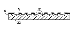
Figure 5b shows a side view of a PB according to
the invention.
CA 02223~38 1997-12-03
W O 96/40507 27 PCT~US9G~7~
Figure 6 is a top view of a PB made in accordance
with the invention.
Figure 6a is a cut away side view of the PB of Fig-
ure 6 taken along lines 6a-6a.
Figure 6b is a cut away side view of the PB of Fig-
ure 6 taken along lines 6b-6b.
Figure 6c is a cut away side view of the PB of Fig-
ure 6 taken along lines 6c-6c.
Figure 6a is a cut away side view of the PB of Fig-
ure 6 taken along lines 6d-6d.
Figure 7 is a schematic view of a prior art system
for making PB's.
D~ta; 1 Q~ Description O$ The Invention
This invention includes -
~ thin film printed board precursors that contain a
thermosetting resin layer and metal foil layer in
direct contact with a side of the resin layer, op-
tionally containing a supporting layer comprising
fiber, fabric and/or thermoplastic polymer, in con-
tact with the other side of the resin layer, and
methods for making such precursors; and
~ thin film printed board precursors that contain
thermoset resin layer and metal film adhesively
bonded directly to a side of the thermoset resin
layer, optionally containing a supporting layer com-
prising fiber, fabric and/or thermoplastic polymer,
in contact with the other side of the resin layer,
the resulting printed boards and methods for making
~he precursors and the printed boards.
The process of the invention creates the electrical
circuit in the PB by a mechanical pressing action that
either debosses or embosses the circuit path on the
board. A master tool has the circuit pattern on it as
raised lines (embossed) or depressed groves
CA 02223~38 1997-12-03
W O 96/40507 28 PCTAUS96/09705
(debossed). The master tool is made by a conventional
photo imaged chemical etch process. A metal tool plate
is covered with a photoresist. U.V. light is shined
through a negative image of the embossed circuit
paths, onto the photoresist, hardening the areas that
will remain after etching. The piece is then treated
to remove the unhardened areas of the photoresist.
When passed through an acid bath (e.g., ferric chlo-
ride solution), the exposed metal of the tool plate is
etched away. The hardened areas of the photoresist
are stripped off leaving a relief image of the em-
bossed pattern to be stamped into the foil.
This pattern is transferred to the PB lamination by
a simple pressing operation. Because mechanical rep-
lication transfers the pattern to the laminate, a much
finer line spacing can be achieved than by photo etch-
ing. This can be turned into a metal circuit by a va-
riety of methods. For example:
l.The raised line (embossed) tool is pressed into cop-
per (or other metal) foil that has been placed over
the adhesive. This can be pressed in seconds and
cured in a later operation, either with the tool in
place or removed.
2.That method may be modified by masking the circuit
line pattern on a silk screen or by stenciling, and
coating the underside of the copper foil, i.e., the
side of the foil that contacts the adhesive, with a
release agent. After the foil is pressed into the
adhesive, and the adhesive is cured, then the foil
over the release agent can be abraded to easily
separate those sections of the foil from the lami-
nate.
The concept of molding a non-conducting thermoset-
ting resin in order to form a PB is best achieved us-
CA 02223~38 1997-12-03
W O 96/40507 29 PCT~S96/09705
ing a thermosetting resin having the properties set
forth herein. Very few thermosetting resin formula-
tions have the capacity to form a thin film possessing
the following collective properties:
~ 5 a) the formulation shapes by processes such as stamping
and compression molding, and the like;
b) the resin formulation is nonconductive, which means
that the formulation can be used as a dielectric
substrate;
c) the formulation forms a thin film that is suffi-
ciently uniform in thickness in order to provide
consistent heat shaping capability across the
breadth of the film, and the thickness should be
sufficient to accept the shape imposed by the shap-
ing process;
d) the formulation can be molded by compression or
stamp molding without the need for constraining flow
at the edges of the resin film;
e) the resulting film possesses low flow over a broad
temperature range so that it does not flow uncon-
trollably while undergoing cure conditions, and when
placed under pressure, only the portions that are
superimposed over a groove or cavity in the case of
a female (debossed) mold, or over a protuberance in
the case of a male (embossed) mold, will be caused
to flow because of pressure imposed on the film; and
f) the resulting film gels or achieves properties simi-
lar to a state of gelation, over conditions Leading
to cure, that satisfy commercial conditions.
The average thickness is preferably from about 1 to
about 250 mils (about 0.00254 cm to about 0.635 cm).
The invention relates also to the use of a thin
isotropic thermosetting resin film with the met~l foil
layer that is amenable to being subjected to t:he de-
CA 02223~38 1997-12-03
W O 96/40507 30 PCTrUS9G/~3iO5
bossing procedure that imparts a printed circuit pat-
tern thereon. These thin isotropic thermosetting
resin films avoid the aforementioned CTE deficiencies
of an anisotropic fabric prepreg. This can be ef-
fected with minimal loss of debossment precision foreventually generating a printed circuit board that is
devoid of CTE mismatch, or for forming a tool useful
in effecting the debossment procedure. The thin iso-
tropic thermosetting resin film/foil laminate has the
capacity of being precision molded with a tool at a
relatively low temperature, such as temperatures as
low as room temperature (~23.5~C.), with superior du-
plication of the pattern.
The invention also contemplates associating with
the foil layer, a thin isotropic film of a thermoset-
ting resin that contains in situ-expandable thermo-
plastic particles that contains an essentially uniform
density and thickness across the breadth of the film.
In this embodiment, pressure built up in the interior
of the film during curing causes the film to expand.
The invention contemplates placing such a film in con-
tact with a debossing stamp containing a replicative
printed circuit pattern and heating the film at a tem-
perature that causes the in situ-expandable thermo-
plastic particles to expand into the debossing stampsurface to generate a debossed pattern in the expanded
film.
The term "isotropic" means, in the context of this
invention, a material possessing essentially the same
electrical and physical properties in all directions
(e.g., x, y and z) through it. This is to be con-
trasted with fabric reinforced prepregs. Such
prepregs are anisotropic. They exhibit several times
differences in properties between the x, y and z di-
CA 02223~38 l997-l2-03
W O 96/40507 3~ PCTnJS96/09705
rections. In the case of this invention, the films do
not exhibit differences in electrical and physical
properties by more than 20% in any direction.
There are many commercial thermosetting resin sys-
tems that can be used to produce a thin pliable adhe-
sive thermosetting resin film. For example, certain
of such films are employed in Synspand~ and Syncore~,
expanded or expandable films that are sold by The Dex-
ter Corporation. However, another of a special subset
of such a resin system is a thin isotropic thermoset-
ting resin film that is amenable to being subjected to
a debossing procedure that imprints a printed circuit
pattern thereon without creating mismatches of coffi-
cient of thermal expansion ("CTE") between the copper
deposited thereon that could result in cracks in
grooves, sockets, pads, etc. Such a resin film should
be capable of effecting debossment precision suffi-
cient to eventually generate a PB or for forming a
tool useful in effecting the debossment procedure
leading to the PB. The thin thermosetting resin film
should have the capacity of being precision debossed,
e.g., stamped, with a tool at a relatively low tem-
perature, such as temperatures as low as room tempera-
ture (~23.5~C.), with superior duplication of the pat-
tern. It is particularly desirable that the thinthermosetting resin film be amenable to a stamping
procedure that debosses a grooved printed circuit pat-
tern thereon with minimal loss of debossment precision
of the grooved pattern. The film should be capable of
retaining the debossed pattern and the grooving
through a cure cycle without flow out within the pat-
tern, to produce a thermoset (i.e., cured) resin film
that is employable for making a printed circuit board.
CA 02223~38 1997-12-03
W O 96/40507 32 PCTrUS96/09705
On the other hand, the thin thermosetting resin
film may be subjected to flow into the grooves and
cavities of a female tool, as defined above, to form a
male replication of the female tool. Or the film may
be shaped and stamped with a tool, subjecting the
resin to temperatures sufficiently high enough to set
the resin (e.g., by gelation, incipient gelation
("near-gelation") or cure) while in contact with the
tool, thereby fixing a surface thereof to replicate
the male or female image of the female or male sur-
face, as the case may be. In this manner, the film of
the invention is convertible into a male or female
tool for making a PB by debossing another film having
the same or similar composition, or the film can be
used as a PB substrate.
The elements of the essentially nonconductive ther-
mosetting resin film is that it is shapable. It has a
thin uniform thickness. It contains a thermosetting
resin that advances to a cured state without forming a
significant volatile byproduct that will affect the
quality of the cured film. It contains one or more
flow control components that allows the film to be
molded without edge flow constraints,1 provides low
flow of the film over a broad temperature range and
retains a debossed image during debossment up to and
through cure of the film. The film advances, under
conditions leading to cure of the thermosetting resin,
to a state of gelation (see IPC-TM-650 Method 2.3.18)
or a condition that gives physical properties similar
to the state of gelation (i.e., incipient gelation) at
temperatures as low as about 20~C. to about 250~C., in
This is to be contrasted with a conventional epoxy resin glass
fiber fabric prepreg which on lamination results in flow of
resin through the edges.
CA 02223~38 1997-12-03
W O 96/40507 33 PCT~US9G/'~70~
less than about 7 days and more than 1 second. Last
but not least, the film exhibits a low dielectric con-
stant (i.e., possesses the ability to resist the for-
mation of an electric field within it) consistent with
the requirements of a PB.
In another embodiment of the invention, the mold-
able, essentially nonconductive thermosetting resin
film is metal platable and adheres to a conductive
metal film. In particular, the film is metal platable
and adhesively bondable to metal foil that can be used
in the making of a stamping surface or for creating a
conductive pathway on the stamped and cured resin
film.
The Th~ -~tting Resin
The typical thermosetting resin is an A-stage
resin. In some cases, it may be desirable to utilize
a B-stage resin but in the typical case, such is done
in combination with an A-stage resin. Such B-stage
resin will affect the viscosity of the resin formula-
tion but they are typically not relied on to achieve
the level of thickening for the most effective opera-
tion of the invention.
Epoxy systems curing in the range from 150"-400~F.
(65.5~-204.4~C.) are common matrix resins for making
thin film thermosetting resin products including the
products of this invention. Matrix resin of bis-
maleimide (BMI), phenolic, polyester, PMR-15 poly-
imide, cyanate ester resins and acetylene terminated
resins may also be used. The most widely used matrix
resins are the epoxy resins, and a wide variety are
suitable for use in the practice of this invention.
Illustrative of such epoxy resins are the following:
CA 02223538 1997-12-03
W O 96/40507 34 PCTrUS96/09705
~ H ~ H, ,OCH,CHCH, ,OCH~CHCH,
CH2CHCH20 ~ OcH~cHcH2o ~ CH ~ H,CHCH, ~ CH, ~
_o~H ~ CH, H,C~CH,
H2 ~ CH2CHCH~ ~ H ~ H2
~ P\ ~ ~ ~N ~ OCH,CHCH2 _ ,CHCH, ,~ CHCH,
CH,CHCH,O CH,CHCH20 CH,CHCH,O CH2CHCH2
CH,CHCH, ~ ,CHCH2 CH2CHCH2/ ~ ~ ~CH,CHi~
CH CHC ~ CHCH2
C~CHcH20(cH2)~ocH2~cH2 CH2CHCH2~CH2--0~0CH2CHCH2 CO~CHCH2
CH20 1~~ ~CH2CHCH2
~ CH2CHCH!'[3 CH2CHCH2~C~ Qlo~ ~
CH2cHcH2oJ3~ocH2cHcH2 CH2CHCH~ --2
O~ ~0~0~0
_ W
~~~~ ~
0~
0~ ~0
The epoxy resins may be modified up to 95 weight
percent by including in the resin formulation bis-aryl
cyanate esters, such as those of the formula:
R,~y,X~R3
NCO ~ ~ OCN
R2 R~
wherein X is a bisphenol linkage and R1,2,3 and ~ are ring
substituents such as hydrogen, alkyl, aryl, and the
like. Illustrative compounds are:
CA 02223~38 1997-12-03
W O 96/40507 35 PCT~S96/09705
NC~OCN NC~ ~OCN
NC~OCN NCJ~OCN
NC~ NC~~C~}OCN
Another preferred resin is one that is totally 1:he re-
action product of one or more of the bis-aryl cyanate
esters.
Catalyst~ and Hardon~rs
The epoxy resin systems contain epoxy curing agents
to form solid, infusible products. For this purpose,
epoxy curing agents that are acidic, neutral or alka-
line may be used. Examples include, among others,
amines hardeners, phenols, acid anhydrides, polyamides
and Lewis acids and bases. Desirably, the epoxy res-
ins of the invention are combined with hardeners that
cure the resin to a thermoset condition. The pre-
ferred hardeners are amine compounds, ranging from di-
cyandiamide, to ureas, to aliphatic and aromaticamines. Preferred are the aromatic amines encompassed
by the formula:
NH2
~ Q~ NH2
wherein Q is one or more of a divalent group such as -
SO2-, -O-, -RaRbC-, -NH-,CO-, -CONH-, -OCONH-, and the
like, Ra and Rb may each independently be one or more of
hydrogen, phenyl, alkyl of 1 to about 4 carbon atoms,
alkenyl of 2 to about 4 carbon atoms, fluorine, cy-
cloalkyl of 3 to about 8 carbon atoms, and the like, x
CA 02223~38 1997-12-03
W O 96/40507 36 PCT~US96/09705
may be 0 or 1, y may be 0 or 1 and is 1 when x is 1,
and z may be 0 or a positive integer, typically not
greater than about 5.
Another preferred class of hardeners are the ali-
phatic amines such as the alkyleneamines. Illustrativeof suitable alkyleneamines are the following:
monoethanolamine, ethylenediamine, N-(2-
aminoethyl)ethanolamine, diethylenetriamine,
piperazine, N-(2-aminoethyl)piperazine, triethyle-
netetramine, tetraethylenepentamine, pentaethylenehex-
amine, diaminoethylpiperazine, piperazinoethylethyle-
nediamine, 4-aminoethyltriethylenetetramine, tetraeth-
ylenepentamine, aminoethylpiperazinoethylethyl-
enediamine, piperazinoethyldiethylenetriamine, and the
like.
Another class of hardeners, which can also be used
as extender of the epoxy resin, are the higher molecu-
lar weight poly(oxyalkylene)polyamines such as those
of the following formulas:
CH3 ,CHJ
H2NCHCH2~0CH2CH)yNH2 whcrc v is 2~0
CH3 CH3 CH3
H2NCHCH2(0CH2CH)~(OCH2CH2)b(0CH2CH)cNH2 wher~ a~c is about 2
andbis8 15.
C, Ha
CH2(OCH2CH)"NH2
CHacH2ccH2(ocH2 ICH)yNH2
CH~ v hcre x, y and z ran~ ~n 2~0
CH2(0CH2 ,CH)~NH2
CH~
CH~ CH~ ,CH3
H2NCHCHz(OCH2CH)mNH(OCH2CH)dNH2 vJlerc n~d is about 82-86.
Preferred hardeners are diamines of the formula:
CA 02223~38 1997-12-03
W O 96/40507 37 PCT~JS9G~705
I~,N~ ~ --0'N~I, ~NH~
~ NH, ~ 2
,_r ~
The hardener may be a monoamine such as aniline,
para-aminophenol, and alkylated versions of them.
Other desirable hardeners are the reaction products of
dialkylamines, such as dimethylamine, diethylamine,
methylethylamine, di-n-propylamine, and the like, with
a variety of mono and diisocyanates to form mono and
diureas. Any of the polyisocyanates listed below may
be so reacted for use as a hardener. Specific illus-
tration of useful hardeners are those encompassed bythe following formulas and descriptions:
~NH~ NR2 ~NH~NR2
NR2 p
R2N N~R~ " 40
NR2
wherein Ry is a monovalent group; Rx is alkyl, halo,
alkoxy, and the like; Rz is methylene, isopropylidene,
ethylidene, or a covalent bond; and s is 0-4.
Preferred urea hardeners are those that are the re-
action products of dimethylamine with mixtures of 80~
2,4-tolylene diisocyanate and 20% 2,6-tolylene diiso-
cyanate, polymeric isocyanate, p-
chlorophenylisocyanate, 3,4-dichlorophenyl- isocyanate
or phenylisocyanate.
CA 02223538 1997-12-03
W O 96140507 38 rCTAJS~G~0~705
Accelerators may also be used and include imida-
zoles and substituted ureas. Examples include 2-
ethyl-4-methylimidazole and p-chlorophenyl-1, 1-
dimethyl urea.
The amount of the hardener employed is usually
stoichiometric on the basis of one amine group per ep-
oxy group in the resin. If the epoxide is a triepox-
ide and the hardener is a diamine, then the molar ra-
tio of hardener to epoxide would typically be about
2.5/3 or 0.83. A typical formulation would have a
weight ratio of epoxy resin to hardener of about 3/2
to about 4/1. Where any of the hardeners serve pri-
marily as extenders of the epoxide resin, then the
amount of the hardener in the typical case will be
less than that generally employed for hardening the
epoxide. Mixtures of the above hardeners and with
other hardeners are within the contemplation of this
invention.
Oth~r U~e~ul P~
As noted above, other reactive resin systems include
the various thermosetting or thermosetting resins in-
clude the bismaleimide (BMI), phenolic, polyester
~especially the unsaturated polyester resins typically
used in SMC production), PMR-15 polyimide, bis-aryl cy-
anate esters and acetylene terminated resins are also
suitable.
A particularly desirable resin for this application
is the vinyl ester resin. This class of resin is based
on the reaction of unsaturated carboxylic acids and ep-
oxy resins or epoxy compounds. Illustrative reactants
in forming the vinyl esters are the following:
CA 02223538 1997-12-03
W O 96/40507 39 PCTrUS96/09705
Ei~oxy R-sin~ Acids:
~ CH, C~11, ~e~cU
~~ OH .... ~, ~_",
o~ ~o ~1~ C~~icAr i
~, ~r oH
O Og g [~ ~ ~0 f~ ~A --
~:~C3 o~~~J~CC ~~~~~ ~
Typical of the vinyl esters are the following:
~~~~~~~~
~o~o~
~3 HO ~
In the above formulae, w is a positive value of from
about 1 to about 20, preferably from about 2 to about
10 .
The vinyl ester resins may be used alone or in combi-
nation with monoethylenically unsaturated monomer.s, such
as styrene, o-methylstyrene, m-methylstyrene, p-
methylstyrene, ethylstyrene, a-vinyl-xylene, a-
chlorostyrene, a-bromostyrene, vinylbenzylchloride, p-
tert.-butylstyrene, methyl methacrylate, ethyl acrylate,
CA 02223538 1997-12-03
W O 96/40507 40 PCTAUS96/09705
propyl acrylate, butyl acrylate, butyl methacrylate,
propyl methacrylate, butyl methacrylate, lauryl acry-
late, 2 - ethyl hexyl acrylate, ethyl methacrylate, and
the like,
C,~,O O~WlOH ~~~ ~)n
HO~J ~~ 0~3n ca~O~~~~
H ~H~0~3n C~~0~~~~~ ~)n
c~o 09 ~o ~0 ~
N~ O~)n ~N~ ~~3n
C~O~ ~0
C~ ~~~ ~)n O HO~;~OH O
'~ ~ ~ C~ ~ $~ (~ HO~ ~n
~H--~ f~,~L
O H ~~ ~ H~~¢o~~~)
diethylene glycol dimethacrylate, 1,4-divinylbenzene,
and the like. In the above, n is O or 1.
A number of vinyl ester resins require the use of
solvents such as methyl ethyl ketone, acetone, toluene,
and the like.
The vinyl esters may be cured by any free radical
mechanism, such as by photoinitiation and/or by use of
peroxidic compounds. A photoinitiator may be included
in the formulation, as an optional ingredient. Light-
initiated curing of the vinyl ester alone or with other
CA 02223~38 l997-l2-03
W O 96/40507 PCTnJ'596/09705
41
polymerizable materials involves photosensitiz;ation of
light-sensitive compounds by ultraviolet or visible light, which,
in turn, initiates polymerization of the resin materials. The
photoinitiator may comprise a combination of a photosensitive
ketone and a tertiary amine. Typical photosensitive ketones
include brenzophenone, acetophenone, thioxanthen-9-one,
9-fluorenone, anthraquinone, 4'-methoxyacetlDphenone,
diethoxyacetophenone, biacetyl, 2,3-pentadione, benzyl,
4,4'-methoxybenzil, 4,4'-oxidibenzil, and 2,3-bornadione (dl
camphroquinone). Typical tertiary amines include
ethyl-4-dimethyl amino benzoate, ethyl-2-dimethyl amino benzoate,
4,4'-bis(dimethylamino) benzoph~no~e, N-methyldiethanolamine, and
dimethylaminobenzaldehyde. Any of the known photosensitizing
system that can function effectively when exposed to light may
substitute for the above-named compounds or co-m-binations. The
amount of the photoinitiator should be sufficient to initiate
polymerization in a selected resin and complete it in depth
within about half a minute when the resin composition is exposed
to a visible-light output of at least 5,000 foot candles. In
addition, any known free-radical scavenger (anti-oxidants) such
as butylated hydroxytoluene caLn be used to scavenge sma,ll amounts
of free radicals generated during extended shelf storage.
The curing of the vinyl ester is primarily effected by a
thermal initiator, which is a typical thermal curing agent known
in the art. Illustrative of these are benzoyl peroxide, dicumyl
peroxide, methyl ethyl ketone peroxide, ditertiary butyl
peroxide, tertiary butyl hydroperoxide, tertia,ry butyl
perbenzoate, Luperox 118 (sold by Wallace and Tiernan, Lucidol
Division, 1740 Military Road, Buffalo, NY 14240), cumene
hydroperoxide, or other suitable peroxides may initiate
polymerization of the polymerizable ethylenically unsaturated
components of the primary coating. For example, Benzoyl peroxide
may be used together with 2-hydroxyethyl-p-toluidine. It is
common to combine metal salts such as metal naphthenates, e.g.,
cobalt naphthenate, and the like, with tertiary ~m;n~, such as
dimethyl aniline, with the peroxidic catalyst.
3~ ,L~ 3
CA 02223~38 1997-12-03
W O 96/40507 PCT~US96/09705
42
The amount of catalyst is typically that amount that
facilitates the cure within less than ten hours at a temperature
greater than 25~C. Generally, the catalyst system will be less
than about 10 weight percent of the resin formulation. As a
rule, the catalyst system will range from about 0.1 to about 8
weight percent of the resin formulation.
Thick~ning
As noted above, thickening of the resin in forming the film
involves the combination in the resin formulation of -
i) one or more electronic grade filler;
ii) a thermoplastic resin that is soluble or partially
soluble in the therm~setting resin;
iii) an elastomer-type polymer that provide discrete
elastomer phases (second phases) in the th~nmosetting resin
matrix;
iv) a thixotrope; and
v) a mixture of two or more of i), ii), iii) and iv).
Illustrative of suitable electronic grade fillers are
aluminum oxides including alumina trihydrate, coated alllm;nl7m
nitrate, silicon carbide, diamond, ground cured fiber reinforced
thermoset resin, as well as a variety of thermoplastic and
thermosetting fibers. The thermoplastic polymer used in forming
these fibers may be made from condensation type polymers,
such as nylon-6,6; nylon-6; nylon-4,6; polyester from
CA 02223~38 l997-l2-03
W O 96/40507 43 PCTrUS96~705
polyethylene terephthalate; KevlarTM polyaramide, poly-
carbonates (viz., poly (2,2-bis (1.4-oxyphenyl) pro-
pane carbonate)); polyarylates (viz., poly (2,2-
bis(1.4-oxyphenyl) propane terephthalate); polyimides;
~ 5 polyetherimides, such as UltemTM 2; polysulfones (see
U.S. Patents No. 4,175,175 and 4,108,837), such as
UdelTM and RadelTM A-4003; the polyethersulfones (see
U.S. Patents Nos. 4,008,203, 4,175,175 and 4,10~,837),
such as VictrexTM 4; polyarylsulfones; polyaryla-
mideimides, such as TorlonTM 5; and the acrylics and
modacrylic fibers; and the like. The thermoplastic
polymer used in providing the thermoplastic polymer
may also be made from condensation type polymers used
in forming the film, such as nylon-6,6; nylon-6; ny-
lon-4,6; polyester from polyethylene terephthalate;
KevlarTM polyaramide; polycarbonates (viz., poly (2,2-
bis (1.4-oxyphenyl) propane carbonate)); polyarylates
(viz., poly (2,2-bis(1.4-oxyphenyl) propane terephtha-
late); polyimides; polyetherimides, such as UltemTM;
polysulfones (see U.S. Patents No. 4,175,175 and
4,108,837), such as UdelTM and RadelTM A-400; the poly-
ethersulfones (see U.S. Patents Nos. 4,0()8,203,
4,175,175 and 4,108,837), such as VictrexTM; po]yaryl-
sulfones; polyarylamideimides, such as TorlonTM; and
the like.
A particularly preferred class of thermoplastic
polymer for providing toughening and as a flow control
2 Available from General Electric Company, Plastics Business
Group, Pittsfield, MA.
3 Manufactured by Amoco Performance Products Inc.
~ Available from ICI Advanced Materials, Wilmington, DE 19897
5 Available from Amoco Chemical Company, Chicago, Ill.
CA 02223~38 1997-12-03
W O 96/40507 44 PCTAJS96/09705
aid for the thermosetting resin formulations are the
polyurethanes of the formula:
N J~ N ~ ' N J~ O-R-OJ~ N IN N (I
H H H _ n H
wherein a and b are each 1, 2 or 3, n is at least 1, X
is a divalent organic radical containing at least two
carbon atoms in which the N's are bonded to different
carbon atoms of X, R is an aliphatic polyester or
polyalkylene oxide wherein
~ the aliphatic polyester is a polyester of an
alkylene diol and an aliphatic carboxylic acid, or a
polycaprolactone polyol, and
~ the alkylene group of the polyalkylene oxide
contains on average greater than three carbon atoms
and not greater than five carbon atoms, and
R~ is an organic aromatic containing group in which the
OH and N bonded to the R~ group is bonded directly to
different aromatic carbon atoms. Synergistic
combinations of the polymer of formula (I) and other
toughener polymers are useful in improving the
toughening properties of the thermosetting resin
formulations for making printed circuit board
composites.
This invention includes the use in the thin film
thermosetting resin formulation of a miscible or
partially miscible linear polyurethane polymer
containing phenolic hydroxyl functionality for
reaction with a thermosetting resin comprising
~ a linear polyurethane of recurring units
containing linear ester or ether moieties or a
combination of ester and ether moieties
CA 02223~38 1997-12-03
W O 96/40507 45 PCTrUS96/09705
~ which are interbonded through urethane gro~ps and
~ uriedo bonded phenolic hydroxyl-containing
terminal groups.
These linear polyurethane toughener polymers may
contain uriedo bonded phenolic hydroxyl-containing
terminal groups of the formula.
(OH)a ~ ~ ~ ~ ~(OH)Ib~ (I)
N ~ X~ O-R-O N~ N N
H H H H H H
_n
wherein a and b are each 1, 2 or 3, n is at least 1,
each X is a divalent organic radical containing at
least two carbon atoms in which the N's are bonded to
different carbon atoms of X, R is an aliphatic
polyester or polyalkylene oxide wherein
~ the aliphatic polyester is a polyester of an
alkylene diol and an aliphatic carboxylic acid, or a
polycaprolactone polyol, and~5 ~ the alkylene group of the polyalkylene oxide
contains on average greater than three carbon atoms
and not greater than five carbon atoms, and
R~ is an organic aromatic containing group in which the
OH and N bonded to the R~ group are bonded directly to
different carbon atoms and the OH is bonded directly
to an aromatic carbon atom. An improved version of
the polymer of formula (I) is the polymer of formula
(II).
~2 _ k4
( ~ )~ I ~ I ~NJ~o.R oJ~N ~ J~ ~(OH) b
H H _ _ x H H _ _y H H
_ n
CA 02223~38 1997-12-03
W O 96/40507 46 PCTrUS96/09705
wherein x and y are 0 or 1, R' is hydrogen or alkyl of
1 to about 3 carbon atoms, and Rl, R2, R3 and R4 are
hydrogen, nitro, halogen or alkyl of 1 to about 4
carbon atoms. In a preferred embodiment of formula
(I), the carbons to which the OH and N are bonded are
separated from each other by at least one aromatic
carbon atom. A more desirable embodiment is a
toughener polymer of the formula:
(HO)a~(R~ N~NJ~N o-R-~HN _ --y H H ~3(0H)b (III)
In this embodiment, Ro1 is a divalent organic group and
c is 0 or 1. In a preferred embodiment of the inven-
tion, with respect to the polymer of formula (II), x
and y are each 1, Rl R2, R3 and R4 are hydrogen, a and
b are 1 and n has a value such that the weight average
molecular weight of the polymer is about 20,000 to
about 120,000. Incorporating this preferred embodi-
ment in formula (III), Ro1 is methylene or c is 0. In
a further preferred embodiment is a polymer having the
formula:
~NJ~N~N O-R~NJ~N NJ3--OH (IV~
H H H H n H H
wherein n has a value such that the weight average mo-
lecular weight of the polymer is about 30,000 to about
110,000 and R is a polyalkylene oxide in which the al-
kylene groups thereof have an average value of about
3.5 to about 4.5 carbon atoms. A most preferred
polyurethane polymer has the formula:
CA 02223538 1997-12-03
W O 96/40507 47 PCT~S96/09705
HO~H H N~4~ o J~NI J~ N NJ3 (V )
wherein n has a value such that the weight average mo-
- lecular weight of the polymer is about 35,000 to about
100,000 and f has a value of at least 1, preferably
from 1 to about 70, more preferably from about 4 to
- 5 about 55, and most preferably from about 6 to about
42. The terminal hydroxyl groups may be in the ortho,
meta or para positions, preferably in the para posi-
tion.
A preferred polyurethane is one having a molecular
weight from about 20,000 to about 120,000, preferably
about 30,000 to about 110,000, and most preferably
about 35,000 to about 100,000, formed by the reaction
of a poly-1,4-butylene oxide diol having a molecular
weight of from about 650 to about 5,000 with a stoi-
chiometric excess of methylene diphenyldiisocyanate
capped by reaction with o, m or p-amino phenol.
The polyurethane polymer suitable for use in the
thermosetting resin film formulation can be a modifi-
cation such as those made by the following reactions:
~N N~N o~oi¦~ ~)b ~ b) ~
ro ~ o ~ o ~ ~t N
CA 02223~38 1997-12-03
W O 96/40507 PCTrUS96/09705
48
~N N~N O~-OJ~ J~OH) l~b) 0~3
--n
HO~ ~OH
These polyurethane polymers are specially capped
linear polyurethanes formed by the reaction of a
diisocyanate of the formula O=C=N-X-N=C=O with an
alkylene diol of the formula HO-R-OH in the molar
ratio (~~C-N-X-N~C-%o R OH) of >1, such that the resulting
polymer equals the value of n as defined above,
followed by the reaction with aminophenolic compounds.
Diisocyanates suitable for use in making the
polyurethanes include the following:
_______ __ ____
bis (4-isocyanatocyclo- 1,2-diisocyanatoethane
_hexyl)methan_____ ____ ____ _
1,3-diisocyanatopropane 1,2-diisocyanatopropane
_1,4=diisocyanatobutane 1,5-diisocyanatopentane
1,6-diisocyanatohexane bis(3-isocyanatoprop-
yl)ether
bis(3-isocyanatopropylJ 1,7-diisocyanatoheptane
_sulfide__________________ _______ __
1,5-diisocyanato-2,2- 1,6-diisocyanato-3-
dimethylpentane _methoxyhexane
ï, 8=diisocyanatooctane 1,5=diisocyanato-2,2,4=
trimethypentane
l,9-diisocyanatononane 1,10-disocyanatopropyl)-
ether of l,4-butylene
___ glycol
l,ll-diisocyanatoundecane l,12-diisocyanatododecane
bis(isocyanatohexyl) sul- 1,4-diisocyanatobenzene
_ide
2,4-diisoc~anatotolylene___2,~-diisocyanatotolylene
__,3-diisocyanato-o-xylene l,_-diisocyanato-m-xylene
_,3-diisocyanato-p-xylene 2,~-diisocyanato-1-
chlorobenzene
2,4-diisocyanato-1- 2,5-diisocyanato-1-
nitrobenzene nitrobenzene
CA 02223~38 1997-12-03
W O 96/40507 49 PCT~S96/09705
__________________ ____ _____ _~
2,2-bis(4- bis(4-
isocyanato)phenylpropane _isocyanato)phenylethane
4,4'-diphenylmethylene 3,3'-diphenyl-methylene di-
diisocyanate _isocyanate
polymethylene isophorone diisocyanate
poly(phenyleneisocyan-
ates)
and mixtures thereof.
The preferred polyisocyanates are TDI, i.e., the
mixture of 80~ 2,4-tolylenediisocyanate and 20% 2,6-
tolylenediisocyanate, or the individual monomer 2,4-
tolylenediisocyanate (2,4-TDI) and 2,6-
tolylenediisocyanate (2.6-TDI) and MDI, i.e., 4,4'-
diphenylmethylene diisocyanate and 3,3'-diphenyl--
methylene diisocyanate, or the individual monomer 4,4'-
diphenylmethylene diisocyanate (4,4'-MDI) or 3,3'-
diphenylmethylene diisocyanate (3,3'-MDI).
The polyalkylene ether or oxide diol comprises a
divalent alkylene oxide moiety wherein the a:Lkylene
groups contain, on average, greater than three carbon
atoms and not greater than five carbon atoms.
Typically, they are based on ethylene oxide, 1,2-
propylene oxide, 1,3-propylene oxide, 1,2-blltylene
oxide, 1,3-butylene oxide, 1,4-butylene oxide, 1,2-
pentylene oxide, 1,3-pentylene oxide, 1,4-pentylene
oxide, 1,5-pentylene oxide, 1,2-hexylene oxide,
generally polymerized alone when the alkylene group
contains greater than 3 carbon atoms, or as mixtures,
so as to form a number average alkylene carbon content
greater than about 3 and as high as about 5,
preferably greater than 3.5 and as high as about 4.5.
Many types of alkylene oxide diols are available for
urethane production but all of those that have an
average alkylene below about 3.5 have too high water
absorption properties for use in high performance
CA 02223~38 1997-12-03
W O 96/40507 50 PCT~US9G~Og705
adhesive applications. Such exclude the polyethylene
oxide diol homo-oligomers and the polypropylene oxide
diol homo-oligomers from consideration in forming the
polyurethane tougheners.
All of the polyalkylene oxide diols used in making
the polyurethane tougheners/flow control aids are
prepolymers of the alkylene oxide(s), created by the
polymerization of the monomeric alkylene oxide. Such
prepolymer formation as well as their reactions to
form polyurethanes is notoriously well known. Of the
prepolymers, a preferred one is based on the
polymerization of l,4-butylene oxide (i.e.,
tetrahydrofuran) to a molecular weight of from about
650 to about 5,000. Such prepolymers are commercially
available from DuPont under the name Terathane~.
Terathanes~ range in molecular weights as low as about
650 to as high as about 2900, as well as molecular
weight versions of about 1000 and 2000. Higher and
lower molecular weight versions are also available.
Such prepolymers provide low water absorption,
flexible molecular structure, hydrolytic stability,
and commercial availability at a moderate cost.
Terathanes~ have the formula HO(CH2CH2CH2CH2O)tH where t
has a value of about 8-9 to about 40, though higher
and lower values are available, and such oligomers
could be used in making the polyurethanes.
Terathanes~ have been widely recommended for use in
making polyurethanes by DuPont. For example, they
have been recommended by DuPont for use in forming
soft segments in polyurethanes. When used with TDI,
DuPont advises that amines such as 4,4'-methylene-
bis(2-chloroaniline) are favored as chain extenders or
curatives. If 4.4'-MDI is the chain extender, DuPont
advises that l,4-butanediol is the favored chain
CA 02223~38 l997-l2-03
W O 96/40507 51 PCT~US9G~7~
extender. However, this invention does not rely on
other monomers as chain extenders or curatives though
chain extenders can be employed to raise the molecular
weight of lower polyurethane prepolymers prior to the
capping step in making the polyurethanes.
The polyester diols useful in making the
polyurethanes are based on the reaction products of an
aliphatic dicarboxylic acid derivative (such .as the
acid halide or ester) and an aliphatic diol derived
from an polyalkylene oxide diol such as an alkylene
glycol of 2 to about 5 carbon atoms, or based on the
reaction of ~-caprolactone with a starter organic
diol. These polyester diols are commercially
available materials. They are typically less
hydrolytically stable than the aforec1efined
polyalkylene oxide diols. Those that are desirable in
the practice of the invention are those that possess
low water absorption, flexible molecular structure,
hydrolytic stability, and commercial availability at a
moderate cost.
The linear polyester resins may be reaction prod-
ucts of saturated and unsaturated aliphatic dicarbox-
ylic acids, such as malonic acid, succinic acid,
adipic acid, maleic acid, fumaric acid, hexahydro or
tetrahydrophthalic acid, "dimer" acid (dimerized fatty
acids), and their respected anhydrides (where chemi-
cally possible), acid halides, and esters, with or-
ganic diols. The polyester may include in the reac-
tion a minor amount, typically not more than 20 mol ~,
preferably not more than 10 mol ~, of the acid compo-
nent of the polyester, of an aromatic dicarboxylic
acid such as o-phthalic acid or anhydride, isophthalic
acid, terephthalic acid, their respected anh~ydrides
(where chemically possible), acid halides, and esters.
CA 02223~38 1997-12-03
W O 96/40507 ~2 PCTAJS96/09705
In addition to the above polyesters one may also use
dicyclopentadiene modified unsaturated polyesters like
those described in U.S. Patent Nos. 3,986,922 and
3,883,612, so long as the polyester is linear. The
organic diol employed to produce the polyester may in-
clude the alkylene glycols such as ethylene glycol,
propylene glycol, butylene glycol, dipropylene glycol,
diethylene glycol, neopentyl glycol, and the like, and
the polyalkylene oxide glycols such as triglyme (b.p.
216~C.), tetraglyme (b.p. 276~C.), tripropylene glycol,
tetrapropylene glycol, and the like.
Chain termination of the linear polyalkylene oxide
or polyester polyurethanes is effected by reacting
more than one mole of the diisocyanate for each mole
of the polyalkylene oxide diol and/or polyester diol.
The amount of the stoichiometric excess of the
diisocyanate will determine the degree of
polymerization (n) of the polyurethane. A
stoichiometric amount of the diisocyanate to the diol
is 1 mole of each. If the reaction is conducted under
anhydrous conditions, using an excess of diisocyanate
over the stoichiometric amount results in a polymer
that is chain terminated with isocyanato groups at
each end. If any water is present in the polyurethane
formation step, then stoichiometry should take that
into account, because water will generate more near-
terminal residing urea, as well as terminating
isocyanato groups appended thereto. The level of
excess diisocyanate will determine the degree of
polymerization and thus determine the value of n in
the above formulas. Such an isocyanato-terminated
polymer is not a thermally or chemically stable
polymer.
CA 02223538 1997-12-03
W O 96/40507 53 PCT~US96/09705
The hydroxy aromatic amino compound for terminating
the isocyanato containing polyurethane is preferably a
structure of the formula:
(HO)a~ (R02)C- N (VI)
wherein the combination of Roo and Ro2 is equivalent to
R~ and Ro1 defined above, and in particular, Roo may be
a covalent bond or a divalent non-aromatic group such
as alkylene, alkylidene, oxygen, carbonyl, sulfone,
and the like, d is 0 or 1 and when it is 1, the
hatched line designating a fused ring bond is
nonexistent, and when d is 0, the hatched li.ne may
exist as a fused ring bond to Ro2. Ro2 is aryl,
polyaryl, fused ring aryl, polyfused ring aryl,
cycloalkyl and the like, and c is 0 or 1. When d is
1, c is 1, and when d is 0, c may be 0 or 1. Ro3 is
hydrogen, or alkyl of 1 to about 14 carbon atoms.
Illustrative examples of suitable amines are the
following:
HO~0~ Ho~l/4 HO 0~ ,~
HOf~ ~IH, HO~N4HO~--N4
HO~3~ HO~ HO~N4
HO~ HO~, HO~
'
The aminophenols, p, m or o-aminophenol, prove to
be effective terminating molecules for the isocyanato
capped polyurethanes. Solubility or a low melting
point gives the meta product some advantage but the p-
CA 02223~38 1997-12-03
W O 96/40507 PCTnJS96/09705
aminophenol dissolves readily in the toughener polymer
- epoxide reaction system at the temperatures gener-
ally used (80-120~C). The low molecular weight of
these aminophenols (109.1) means that relatively small
amounts can be used for termination, solubility is
high, the termination reaction is rapid, governed
mostly by the time required to get good dispersion in
the high viscosity system. The powdered amino phenol
can be added directly to the reaction mixture or more
desirably can be powdered, mixed with a small portion
of the low oligomer epoxide resin diluent, discussed
below, and then added. Measurement of the IR absorp-
tion ratio of the isocyanate group 2240 cm l peak to
the 2840 cm~1 -CH peak can be used to ensure that ter-
mination is complete.
During the polymerization of diisocyanates with the
hydroxy terminated alkylene oxide or polyester based
materials, high molecular weights are attained (~2OK-
~120K, more typically in the range of about 30K to
about lOOK). As a result, viscosities became very
high and at rational reaction temperatures (~50-170~C,
preferably from about 80~C.-120~C.) stirring in
laboratory or production equipment can become
difficult. Use of a solvent as a diluent (e.g.,
methylethylketone (MEK), tetrahydrofuran (THF), and
the like) of the reactants and the reaction products,
though usable in making the polymers of the invention,
adds the problem of its subsequent removal with a
concomitant increase in production cost. Advantage is
- 30 taken of the very low reactivity of hydroxyl groups
with epoxide groups (unless catalyzed) and also the
low reactivity of isocyanate groups with epoxide
groups (unless the complex formation of oxazolidone is
deliberately forced). Therefore, oligomer-free and
CA 02223~38 1997-12-03
W O 96/40507 55 PCT~US9C~5705
thus secondary hydroxyl-free, epoxide resins can be
used as unreactive diluents during the polymer
formation. Such epoxide resins are subsequently
compatible with formulation needs in future adhesive
systems. For this dilution during reaction, epoxides
as free as possible from oligomers should be used.
Shell's Epon~ 825 (the diglycidyl ether of biesphenol
A) has been successfully used as a diluent: even
although the small amount of oligomer present (5~) did
show some reaction. At 1/1 ratio to total clerived
polymer, Epon~ 825 gave polymer products easily
stirred at needed production temperatures and at that
level should meet most subsequent formulation needs.
D.E.N.~ 332 from Dow Chemical should also be suitable.
The Bis F resins, such as Epiclon~ 830S, if distilled
to eliminate oligomers, could also be used.
Illustrative of suitable diluents are epoxy
monomers and dimers of the following formula:
R' R'
0~0 ~0 ~0 ~0--~0
OH
wherein Ra and Rb are each hydrogen, alkyl of 1-3 car-
bon atoms or phenyl, preferably alkyl such as methyl,
and p has a value of 0 to <1, preferably less than
about 0.2. Most preferably, p is equal to 0.
The reaction conditions for forming the
polyurethane from the diisocyanate and the dioL is a
temperature of about 50~C. to about 200~C. with mixing
in the presence of a diluent, such as a conventional
solvent, as indicated above, or the reactive diluent
comprising the epoxy monomeric resin indicated above.
The reaction should be carried out in the absence of
CA 02223~38 1997-12-03
W O 96/40507 56 PCT~US96/09705
added water, and anhydrous conditions are preferred.
Conditions that remove water from the reactants before
reaction and during reaction are desirable. No
special catalysts are needed to effect the reaction
but a catalyst that does not adversely affect the
reactions can be employed. Catalysts are needed in
polymerization reactions using aliphatic isocyanates.
The foregoing polyurethanes and their manufacture
are described in commonly assigned copending U.S.
Application S.N. 08/349,876, filed December 6, 1994.
Another class of flow control aid thixotropic
agents and/or elastomer-type polymers that provide
discrete elastomer phases (second phases) in the ther-
mosetting resin matrix. Certain of these materials
may reduce, to some finite degree, the crosslinking
density of the thermoset resin (C-stage). Many of
these materials introduce very favorable properties to
the resulting thermoset resin. For example, a par-
ticularly desirable material for this purpose, is an
elastomeric polymer containing soft and hard segments,
the hard segments acting like or forming on process-
ing, crosslinking of the elastomeric type. Some of
these elastomeric types contain functional end groups
that allow it to couple with complementary functional
monomers or polymers to form the desired elastomer in
situ of the thermosetting resin and render it non-
pourable and tacky, while toughening the cured resin.
As a class, these elastomeric polymers act or are
crosslinked yet are thermoprocessable, which when dis-
cretely provided in the matrix resin render the resinnon-pourable and tacky, and also toughens it.
One class of suitable elastomer-type thermoplastic
ABS (acrylonitrile-1,4-butadiene-styrene) block co-
polymers that are typically used as modifiers of other
CA 02223~38 1997-12-03
W O 96/40507 57 PCTrUS961~g7~5
resin systems. They are characterized as having a
wide range of properties though the preferred systems
of the invention utilize copolymers that are high rub-
ber types that, when compared to other copolymers of
this type, have a relatively low tensile st3ength,
low tensile modulus, higher impact resistance, low
hardness and heat deflection temperature.
Another elastomer that is found desirable are the
carboxyl and amine terminated liquid butadiene acrylo-
nitrile copolymers. Such copolymers may contain pen-
dant carboxyl groups in the interior of the polymer
structure through the inclusion of methacrylic or
acrylic acid in the polymerization or through t:he hy-
drolysis of some of the pendant nitrile units. Such
polymers react with the epoxy resin and as a result,
the epoxy forms the hard segment generating the elas-
tomer properties.
Another class of block thermoplastic elastomers is
Kraton~, available from Shell Chemical Company. These
thermoplastic rubber polymers possess usable thermo-
plastic properties. They can be softened and they
flow under heat and pressure. They then recover their
structures on cooling. The chemical make-up are of
three discrete blocks of the linear or A-B-A type.
They are available as styrene-butadiene-styrene (S-B-
S) block copolymers, styrene-isoprene-styrene (S-B-S)
block copolymers and styrene-ethylene/butylene-styrene
(S-EB-S) block copolymers. They are characterized by
styrene polymer endblocks and an elastomeric midblock.
After processing, the polystyrene endblocks physically
crosslink, locking the rubber network in place. This
physical crosslinking is reversible on heating.
Another series of the Kraton~ thermoplastic ~ubbers
are the diblock polymers in which one block is a hard
CA 02223~38 1997-12-03
W O 96/40507 58 PCT~US96/09705
thermoplastic and the other is a saturated soft elas-
tomer. Illustrative of this series is Kraton~ G 1701,
a diblock polymer of a hard polystyrene block and a
saturated, soft poly(ethylene-propylene) block.
Other rubbers or elastomers include: (a) homopoly-
mers or copolymers of conjugated dienes having a
weight average molecular weight of 30,000 to 400,000
or higher as described in U.S. Pat. No. 4,020,036, in
which the conjugated dienes contain from 4-11 carbon
atoms per molecule such as 1,3-butadiene, isoprene,
and the like; (b) epihalohydrin homopolymers, a co-
polymer of two or more epihalohydrin monomer, or a co-
polymer of an epihalohydrin monomer(s) with an oxide
monomer(s) having a number average molecular weight
(Mn) which varies from about 800 to about 50,000, as
described in U.S. Pat. No. 4,101,604; (c) chloroprene
polymers including homopolymers of chloroprene and co-
polymers of chloroprene with sulfur and/or with at
least one copolymerizable organic monomer wherein
chloroprene constitutes at least 50 weight percent of
the organic monomer make-up of the copolymer as de-
scribed in U.S. Pat. No. 4,161,471; (d) hydrocarbon
polymers including ethylene/propylene dipolymers and
copolymers of ethylene/propylene and at least one non-
conjugated diene, such as ethylene/ propylene/ hexadi-
ene/ norbornadiene, as described in U.S. Pat. No.
4,161,471; (e~ conjugated diene butyl elastomers, such
as copolymers consisting of from 85 to 99.5% by weight
of a C4-C5 isolefin combined with 15 to 0.5% by weight
of a conjugated multi-olefin having 4 to 14 carbon at-
oms, copolymers of isobutylene and isoprene where a
major portion of the isoprene units combined therein
have conjugated diene unsaturation, as described in
U.S. Pat. No. 4,160,759.
CA 02223~38 1997-12-03
W O 96/40507 59 PCTNS96/09705
Specific illustrations of suitable elastomeric
polymers are the following:
1. HycarTM CTBN liquid reactive rubbers, carboxyl ter-
minated butadiene-acrylonitrile copolymers sold by B.
F. Goodrich.
2. HycarTM CTBNX, similar to CTBN except that they con-
tain internal pendant carboxyl groups, aIso supplied
by B. F. Goodrich.
3. HycarTM ATBN, amine terminated butadiene-
acrylonitrile copolymers sold by B. F. Goodrich.
4. K 1102-28:72 styrene:butadiene linear SBS polymer,
available from Shell
Chemical Company as Kraton~ 1102.
5. KDX 1118-30:70 styrene:butadiene copolymer contain-
ing 20% SBS triblock and 80~ SB diblock, available
from Shell Chemical Company as Kraton~ DX 1118.
6. KG 1657-14:86 styrene:ethylene-butylene:styrene co-
polymer available from Shell Chemical Company as Kra-
ton~ G1657.
7. S 840 A-Stereospecific 43:57 styrene-butadlene SB
rubber available from
Firestone Synthetic Rubber & Latex Company as Stereon~
840A.
8. SBR 1006-random 23.5:76.5 styrene:butadiene SB
block copolymer rubber available from Goodrich Chemi-
cal Company as Ameripol~ 1006.
9. SBR 1502-Random 23.5:77.5 styrene:butadiene rubber
available from Hules Mexicanos, or from Goodrich Rub-
ber Company as Ameripol~ 1502.
10. Blendex~ modifier resins (e.g., 305, 310, 311,
336, 338 and 405) - ABS polymers sold by General Elec-
tric. Different varieties are available and their
suitability depends on the properties sought.
CA 02223~38 1997-12-03
W O 96/40507 60 PCTAUS96/09705
Additional flow reductions are provided by thixo-
troping agents such as fumed silica. Illustrative of
thixotropic agents are high surface area fumed silicas
and organosilyl blocked fumed silicas, and the like.
The thin film may be characterized as non-pourable.
Optionally, the film may be tacky as well. This con-
dition can be achieved in a number of ways. Many
thermosetting resins are solids at about 23~C. and
many of them are liquids at this temperature. Both
kinds of resins can be made fluid non-pourable and
tacky. For example, a resin that is solid and a resin
that is liquid can be combined to form a mixed resin
system that is non-pourable and tacky. In addition, a
solid or liquid thermosetting resin can have incorpo-
rated in it a variety of diverse materials that will
render the resin fluid non-pourable at conventional
handling temperature conditions and fluid non-pourable
and tacky at room temperature (about 15-37~C.). Con-
ventional handling temperatures are defined as a tem-
perature of between about -20~C. to about 43OC.6
Though the in situ-expandable thermoplastic parti-
cles or the solid chemical blowing agent will render a
liquid thermosetting resin more viscous, they alone
are not effective for making the film non-pourable.
If the thermosetting resin is solid, it can be calen-
dered into a film by melting the resin with heat under
conditions that avoid condensation or addition of the
resin to a thermoset condition (C-stage). If the
resin is a liquid, it can be blended with thixotropic
agents, other solid resins and/or liquid or thermo-
6 This range reflects the fact that material h~n~ g can re-
quire low temperature storage to preclude premature reaction of
the thermosetting resin system and relatively high temperatures
because the film may be used on a hot factory floor.
-
CA 02223~38 l997-l2-03
W O 96/40507 61 PCTrUS9GI'~57~
plastic elastomeric modifiers to convert the resin
from a liquid to a non-pourable and tacky material.
The thermoplastic polymer used in forming the in
situ-expandable thermoplastic particles are readily
prepared from a wide variety of materials. A number
of patents refer to their manufacture. For example,
U.S. Patent No. 3,615,972 describes their preparation
by polymerizing the monomer of an aqueous dispersion
of (1) organic monomeric materials suitable for polym-
erization to a thermoplastic resinous material having
the desired physical properties, (2) a liquid blowing
or raising agent which exerts a little solvent action
on the resulting polymer, and in a quantity in excess
of that which is soluble in the polymer, and (3) a
dispersion stabilizing material that is utilized to
maintain the dispersion. The resulting solid spheri-
cal particles have a quantity of the liquid-blowing
agent encapsulated in them as a distinct and separate
phase.
The thermoplastic polymers are formed by the polym-
erization of one or more of a variety of different
types of alkenyl monomers, such as those of the for-
mula:
Rox
I
CH2=C-X,
to form homopolymers or copolymers, such as random or
ordered (including block) copolymers. In the above
OX
formula, R may be hydrogen, alkyl, such as methyl,
~ ethyl and the like, or halogen, such as chlorine,
fluorine, bromine or iodine, and X1 may be an aromatic
containing moiety bonded via an aromatic carbon atom,
a carbonyl oxy ester moiety, halogen, cyano, oxycar-
bonyl ester, carboxyl, and the like. Illustrative of
CA 02223~38 1997-12-03
W O 96/40507 62 PCTAJS96/09705
these monomers are those in which X1 is aromatic con-
taining, such as styrene, o-methylstyrene, m-
methylstyrene, p-methylstyrene, ethylstyrene, a-vinyl-
xylene, a-chlorostyrene, a-bromostyrene, vinylbenzyl-
chloride, p-tert.-butylstyrene, and the like. Also
illustrative of these monomers are those in which Xl is
a carbonyl oxy ester moiety to form acrylate monomers
alone or in combination with the alkenyl aromatic
monomers may also be utilized. Such acrylate-type
monomers include methyl methacrylate, ethyl acrylate,
propyl acrylate, butyl acrylate, butyl methacrylate,
propyl methacrylate, butyl methacrylate, lauryl acry-
late, 2 - ethyl hexyl acrylate, ethyl methacrylate,
OX
and the like. X1 and R may be a halogen, such as
chlorine, fluorine, bromine and iodine, thereby to en-
compass the formation of copolymers of vinyl chloride
and vinylidene chloride, acrylonitrile with vinyl
chloride, vinyl bromide, and similar halogenated vinyl
compounds. X1 may be a cyano group and this includes
polymers of acrylonitrile and methacrylonitrile. X
may be an oxycarbonyl ester, such as the vinyl ester,
e.g., vinyl acetate, vinyl butyrate, vinyl stearate,
vinyl laurate, vinyl myristate, vinyl propionate, and
the like, are suitable polymeric components. One may
also employ for specific purposes ethylenically un-
saturated copolymerizable acids such as acrylic acid,
methacrylic acid, itaconic acid, citraconic acid,
maleic acid, fumaric acid, vinylbenzoic acid, and the
like.
The thermoplastic polymers may also include copoly-
mers (of the random or ordered varieties, especially
blocked copolymers) of the monomers described above
with a variety of hydrocarbon monomers, such as pro-
pylene, butene, and one or more dienes, such as:
CA 02223~38 1997-12-03
W O 96/40507 63 PCT~US96/09705
~ straight chain acyclic dienes such as: 1,4-
hexadiene, 1,6-octadiene, and the like;
- ~ branched chain acyclic dienes such as: 5-methyl-
1,4-hexadiene, 3,7-dimethyl-1,6-octadiene, 3,7-
- 5 dimethyl-1,7-octadiene and the mixed isomers of di-
hydro-myrcene, dihydroocinene, and the like;
~ single ring alicyclic dienes such as: 1,4-
cyclohexadiene, 1,5-cyclooctadiene, ~ 1,5-
cyclododecadiene, and the like;
~ multi-ring alicyclic fused and bridged ring dienes
such as: tetrahydroindene, methyltetrahydro:indene,
dicyclopentadiene, bicyclo-(2,2,1)-hepta-2,5-diene,
alkenyl, alkylidene, cycloalkenyl and cycloalkylid-
ene norbornenes such as 5-methylene-2-norbornene
(MNB), 5-ethylidene-2-norbornene (ENB), 5-propyl-2-
norbornene, 5-isopropylidene-2-norbornene, 5-(4-
cyclopentenyl)-2-norbornene, 5-cyclohexylidene-2-
norbornene, and the like.
The thermoplastic polymer used in forming the in
situ-expandable thermoplastic particles may also be
made from condensation type polymers, such as nylon-
6,6; nylon-6; nylon-4,6; polyester from polyethylene
terephthalate; Kevlar~ polyaramide; polycarbonates
(viz., poly (2,2-bis (1.4-oxyphenyl) propane carbon-
ate)); polyarylates (viz., poly (2,2-bis(1.4-
oxyphenyl) propane terephthalate); polyimides; poly-
etherimides, such as UltemTM; polysulfones (see U.S.
Patents No. 4,175,175 and 4,108,837), such as UdelTM
~ and RadelTM A-400 the polyethersulfones (see U.S. Pat-
ents Nos. 4,008,203, 4,175,17S and 4,108,837), such as
VictrexTM; polyarylsulfones; polyarylamideimides, such
as TorlonTM; and the like.
CA 02223~38 1997-12-03
W O 96/40507 64 PCTAJS96/09705
A wide variety of blowing or raising agents may be
incorporated within the polymerization system. They
can be volatile fluid-forming agents such as aliphatic
hydrocarbons including ethane, ethylene, propane, pro-
pylene, butene, isobutylene, neopentane, acetylene,hexane, heptane, or mixtures of one or more such ali-
phatic hydrocarbons having a molecular weight of a
least 26 and a boiling point below the range of the
softening point of the resinous material when satu-
rated with the particular blowing agent utilized.
Other suitable fluid-forming agents are the chloro-
fluorocarbons such as those described in U.S.
3,615,972 (column 4, lines 21-30) and tetraalkyl
silanes such as tetramethyl silane, trimethylethyl
silane, trimethylisopropyl silane and trimethyl-n-
propyl silane. As pointed out in this patent, the
boiling point of such foaming agents at atmospheric
pressure should be about the same temperature range or
lower than the softening point of the resinous mate-
rial employed.
Blowing agents such as the Freons~, such astrichlorofluoromethane, hydrocarbons such as n-
pentane, i-pentane, neo-pentane, butane, i-butane,
azodicarbonamide are commonly suggested blowing agents
found in these types of in situ-expandable particles.
Typically, the unexpanded particles contain from about
3 to about 40 weight % blowing agent.
As pointed out in U.S. Patent No. 4,397,799, pat-
ented August 9, 1983, the particle size of the unex-
panded particles, as well as the expanded microspherescan vary widely. Particle sizes for the unexpanded
particles can range, for example, from about 1 ~m to
about 1 mm, preferably from about 2 ~m to about 0.5
mm. One version of in situ-expandable particles is
CA 02223~38 1997-12-03
W O 96/40507 65 PCTAUS9G1~5,~5
sold under the name Expancel~, by Nobel Industries
Sweden, Sundsvall, Sweden (U.S. address: Marrietta, GA
30062). They range in unexpanded particle size from
about 5 ~m to about 50 ~m. The particle diameters ex-
pand 2 to 5 times.
Preferably, the in situ-expandable particles used have
a mixed particle size of wide spread to achieve the
- best packing, on expansion, in the syntactic molded
foam. A particularly preferred in situ-expandable
particle is Expancel~ 091 DU, which is believed to be
a terpolymer of vinylidene chloride, acrylonitrile and
methacrylonitrile containing 10-18 weight % isopen-
tane, and possesses the following properties: average
unexpanded particle size of about 12 ~m with a spread
of about 5-50 ~m; true density (expanded in water at
100~C., kg/m3), <20; TMA - T(start) ~C., 1~5-130;
T(max) ~C., ~183; TMA-density,kg/m3, <17.
The chemical blowing agent particles (with a parti-
cle size ranging from about 1 ~m to about 1 mmL" pref-
erably from about 2 ~m to about 0.5 mm) that can beincorporated are inorganic and organic solid composi-
tions that typically decompose at a particulaLr tem-
perature to generate a volatile (gas) component that
causes microcell formation in the thermosetting matrix
resin. Typical inorganic blowing agents include the
ammonium carbonates and bicarbonates, alkali metal
carbonates and bicarbonates such as lithium carbonate,
sodium carbonate, potassium carbonate, rubidium car-
bonate, cesium carbonate, lithium bicarbonate, sodium
bicarbonate, potassium bicarbonate, rubidium bicarbon-
ate, cesium bicarbonate, mixture of the carbonates and
bicarbonates as well as mixtures of the alkali metal
form of the carbonates and bicarbonates. These car-
CA 02223~38 1997-12-03
W O 96/40507 66 PCT~U5~C~
bonates and bicarbonates can be made to decompose at
lower temperatures by incorporating organic carboxylic
acids and acid anhydrides blowing agent accelerators
into the formulation. Suitable organic carboxylic ac-
ids and anhydrides are citric acid, acetic acid and
anhydride, maleic anhydride, There are a variety of
chemical blowing agents sold under the name Celogen~
(Naugatuck Chemical Division of U.S. Rubber Company
(Uniroyal)) that include toluene sulfonyl hydrazide,
toluene sulfonyl semicarbazide, 5-phenyl tetraazole,
azodicarbonamide, and the like, that are excellent
chemical blowing agents suitable for the purposes of
the invention. The chemical blowing agents may be em-
ployed in the formulations of the invention in amounts
ranging from about 0.1 to about 3 parts by weight,
preferably from about 0.5 to 2.0 parts by weight, of
the thermosetting resin formulation.
Lo~ Pro~ilQ Additives
There may be incorporated into the thermosetting
resin formulation certain thermoplastic materials known
in the field as low profile additives. These can be
polymers of vinyl acetate, acrylics, saturated polyes-
ters, polyurethanes, styrene-butadiene and similarly
used materials.
Suitable thermoplastic vinyl acetate polymer low pro-
file additives are thermoplastic poly(vinyl acetate) ho-
mopolymers and copolymers containing at least 5 weight
percent vinyl acetate. Such polymers include, for exam-
ple, vinyl acetate homopolymer; carboxylated vinyl ace-
tate polymers include copolymers of vinyl acetate and
ethylenically unsaturated carboxylic acids, such as
acrylic acid, methacrylic acid, maleic acid, fumaric
acid, itaconic acid and the like or anhydrides such as
maleic anhydride; vinyl acetate/vinyl chloride/maleic
acid terpolymer, and the like. Reference is made to
CA 02223~38 1997-12-03
W096/40507 67 PCT~3S9GI~70~
U.S. Patent Nos. 3,718,714 and 4,284,736 and British
Patent No. 1,361,841 for descriptions of some of the
suitable vinyl acetate polymer low profile additives.
The useful vinyl acetate polymer low profile additives
ordinarily have molecular weights within the range of
from about 25,000 to about 175,000. Suitable polyvinyl
acetate low profile additives are LP-40 and LP-40A that
are sold by Union Carbide Chemical & Plastics Corp.,
Danbury, CT.
Suitable thermoplastic saturated polyester low pro-
file additives are, in general, low molecular weight
saturated polymers of polymerizable linear and/or cyclic
esters and carboxylated saturated polymers and said po-
lymerizable esters having at least one carboxy] group
per molecule. Polymer of linear and/or cyclic esters
including carboxylated polymers having an average of at
least one carboxyl group per molecule that maybe ~used in
accordance with the present invention are those which
possess a reduced viscosity of at least about 0.1, and
preferably from about 0.15 to about 15 higher. The pre-
ferred polymers of cyclic esters have a reduced viscos-
ity of about 0.2 to about 10.
Thermoplastic saturated polymers of linear and/or cy-
clic esters are well known and the carboxylated satu-
rated esters are well known and such thermoplastic satu-
rated polymers, and particularly polymers prepared from
epsilon caprolactones, have been advantageously e3~ployed
as low profile additives. Reference, for example is
made to U.S. Patent Nos. 3,549,586 and 3,668,178 for de-
scriptions of thermoplastic saturated polyester low pro-
file additives and carboxylated thermoplastic saturated
polyester low profile additives prepared from cycLic es-
ters.
Other thermoplastic saturated polyesters that are
useful as low profile additives are those based on con-
CA 02223~38 1997-12-03
W O 96/40507 68 PCTAJS96/09705
densation products of, primarily, dicarboxylic acids and
organic diols. Some examples of such diacids are adipic
acid, isophthalic acid, terephthalic acid and the like
and such glycols could be ethylene glycol, diethyl gly-
col, neopentyl glycol and the like.
Also suitable in certain aspects of the invention are
thomoplastic polyalkyl acrylate or methacrylate low pro-
file additives including, for example, homopolymers of
methyl methacrylate, ethyl methacrylate, butyl methacry-
late, methyl acrylate, ethyl acrylate; copolymers of
methyl methacrylate and lower alkyl esters of acrylic
and methacrylic acids, and copolymers of methyl meth-
acrylate with minor amounts of one or more of the fol-
lowing: lauroyl methacrylate, isobornyl methacrylate,
acrylamide, hydroxyethyl methacrylate, styrene, 2-
ethylhexyl acrylate, acrylonitrile, methacrylic acid,
polystyrene, styrene copolymers, such as sty-
rene/butadiene copolymers, cellulose acetate butyate,
alkylene oxide polymers, urethane polymers, and the
like.
Molecular weight of the alkyl acrylate or methacry-
late polymers useful in the invention may vary over a
wide range from 10,000 to 1,000,000 and preferably from
25,000 to 500,000.
Urethane polymers that can be employed in this inven-
tion, alone or as mixtures with other low profile addi-
tives, are broadly structured and some examples can be
found in U.S. Patent No. 4,035,439; EP 74-746; and U.S.
Patent No. 4,421,894.
The low profile additives may usually be employed in
the compositions of the invention in proportions from
about 1 to 25 weight percent, and preferably from about
5 to 20 weight percent, based upon the total weight of
thermosetting resin, low profile additive and other re-
active components.
CA 02223~38 1997-12-03
W O 96/40507 69 PCTAJ59G~ 70~
The low profile additive can function alone or in
combination with other thickening agents, as a thicken-
ing contributor to the flow characteristics of the
resin.
The thin film may be characterized as non-pourable.
Optionally, the film may be tacky as well. This condi-
tion can be achieved in a number of ways. Many thermo-
setting resins are solids at about 23~C. and many of
them are liquids at this temperature. Both kinds of
resins can be made fluid non-pourable and tacky. For
example, a resin that is solid and a resin that is liq-
uid can be combined to form a mixed resin system that is
non-pourable and tacky. In addition, a solid or liquid
thermosetting resin can have incorporated in it a vari-
ety of diverse materials that will render the resin
fluid non-pourable at conventional handling temperature
conditions and fluid non-pourable and tacky at room tem-
perature (about 15-37~C.). Conventional handling tem-
peratures are defined as a temperature of between about
-20~C. to about 430C.7
Typical formulations of the invention are set forth
in the following tables.
A typical resin formulation comprises the following:
7 This range reflects the fact that material h~n~l ;nq can require
low temperature storage to preclude premature reaction of the the
~etting resin system and relatively high temperatures bec:ause the
film may be used on a hot factory floor.
CA 02223~38 1997-12-03
W O 96/40507 70 PCTrUS96/09705
Component ¦ Typical Components ¦ Range (%w/w)
Resin
A mixture of di- and Novolac Epoxy
multi-functional res- Bis A epoxy
ins selected to give a Bis F epoxy
desired level of vis- Tris epoxy
cosity, tack and glass Brominated epoxy 5-60
transition tempera-
ture.
Fir~ Retardant Filler~
Filler(s) that en- Decabromobiphenyl
~ hances the fire re- Melamine pyrophos- 0-40
tardancy of the for- phate
mulation.
Wetting Agent
Selected to promote
complete wetting of
filler by the resin Non-ionic Surfac- 0.0-1.0
component. tant
TO-~h~n~
An elastomeric mate- ABS Polymers 0.0-10.0
rial selected to im- Silicone Polymers
prove durability
FillQr
Amorphous silica par-
ticulates added to re- Amorphous Silica 25-90
fine cured CTE.
Curing Agent
Aromatic Amines,
Amine, phenolic and/or Guanides, Novolacs, 50-125% Stoi-
homopolymerization Imidazoles, Imida- chiometry,
catalysts zole Salts, 0.01-2.5%
Phosphines. Catalyst
Thixotrope
¦Fumed Silica
Flow control agent ¦Treated Clays ¦0.0-5.0
Specific representative illustrations of such film for-
mulations are the following:
CA 02223538 l997-l2-03
W O 96/40507 71 PCT/U5~/0~705
Weight %
C~ ~ on~nt Arlh~Q;VeAr3h~;vQ ~h9~;VO ~rlh95;Ve
A B C D
Epon 828 (1) 8.5 --- --- ---
Tactix 742 (2) 12.7 --- --- ---
Wcight ~
Component Adhesive Adhesive Adhesive Adhesive
P B c D
Tactix ~9~,'~, 1'.- --- --- ---
DEN ~3 ~ . 21.6 16.438.8
Epiclon 8~
MY ' ~ ~ ------ .0
Pc 1 ~ --- . .. 0.4
Blendex . 8.5 ,. ~. ---
Novaci-e ,, ~ 42.4 --- --- ---
(- 6.2 --- ___
Teco-S-_ 2 ' --- 55.6 70.127.1
,':'. '
TS 720 , '. O.f :.. ' 1.2
4,4'-DDS ~ 5. ~. ---
Dicy _~ J- ~
BTDA _ l - - - - - - - - - 3:.
2 - MI -Azine ,_f --- --- --- ... Tota_ 100.0 100.0 100.0 10 .
%-.esin 4~. 26.~ 2 .' 3 .
% Wetting ~gent
% Tougnener .~
; Filler 4~ 6 . 7C....... 2 .
~ Th_xotrope ~ .~ 1....... ..
Notes:
(1) BiJ A b~od ~5) Bi~ F rc~in, (9) 8ilic~ powdbr, (13) 4,4,_
ro~in, Sholl r-inirpon Ink M lvorn Corp A;- 'nAAir' ~1-
r ~-l Co sulfonQ, Cib~
________________ C~igy
(2) Tri~ opoxy (6) ~p~Yi Ai ~ 0) Silica po~- (14) Dicy ndi~-
r-~in, Dow Ch~mi- Arom~tic ~mino, dsr, ~ mid-, Air P ~d~L.
cal Co Cib~ Cnigy Walkor
____ - , - - , - ~p (7) ~ i ~ni C ~Ur- (ll) Silic~ pow- ~ - - - ~ ~ ~~ ~ ~ ~ ~ ~
oxy r-~in, Dow ~ct~nt, Monr~nto dur, OE Mi 1~ n~ ldo
~ 1 Co. __ __
(4) rr~jAj~ ) ABS t_ _ ~~, (12) Fumad ~ilic~, (16) M~thylimid~-
phonol novol~c, Gonor~l ~l-ctric C~bot zol~-Arinl~ C~t~-
Dow ~l Co ly~t
These resin formulations are made by conventional
m; xi ng of the components in standard mixing equipment
for viscous compositions. Good results have been ob-
tained using a Ross~ Double Planetary Mixer, provided
with vacuum construction and jacketing to control tem-
perature and deaerate the mixture. Mixing i'3 typi-
cally effected by blending the resin, unexpanded par-
CA 02223~38 1997-12-03
W O 96/40507 72 PCTAJS96/09705
ticles, elastomer components, extenders, diluents,
curing agent and vacuum pumping to remove entrained
air. The temperature chosen is variable depending on
the viscosity of the formulation. It may be desirable
5to separately mix the resin and the curing agent. In
such a case, the formulation may be divided up to mix
the resin with some portion of the formulation to ef-
fect a well dispersed condition and do the same with
the curing agent, and then combine the well dispersed
10mixes, so as to mix them all under conditions avoiding
premature reaction. Such procedures are well within
the skill of the art.
The following discussion relates to the drawings
and the figures shown therein. None of the figures
15show true dimensions of the various components there
depicted. Figure 7, which relates to a prior art
process for making flat board PB's, describes unroll-
ing glass fiber fabric from fiber glass fabric roll
111, passing continuous sheet 113 of glass fiber fab-
20ric into resin trough 115 via guide rollers 117, over
guide roller 119 and under guide roller 121. The num-
ber of guides shown is symbolic and not necessarily
indicative of how the resin impregnation step is spe-
cifically carried out. Trough 115 contains sufficient
25A-stage thermosetting resin to allow the desired im-
pregnation of the fabric. The fabric withdrawn from
trough 115 is fed through squeeze rolls 123 set to nip
fabric 125 and reduce the level of resin therein.
Fabric 125, containing A-stage thermosetting resin, is
30fed to treater 127 containing heater 133. Fabric 125
is fed over guide roller 129, past heater 133 and then
over guide roller 131. In treater 127, polymerization
of the A-stage resin is initiated so that the thermo-
setting resin in fabric sheet 135, is transformed to a
CA 02223~38 1997-12-03
W O 96/40507 73 PCTAJS96/09705
B-stage resin. Prepreg fabric sheet 135 is guided by
roller 137 to collection roll 139. The prepreg fabric
135 is, at a separate station, unrolled and cut to
sized individual sheets 141. They are then superim-
posed to form a multi-layer pre-laminate lay-up struc-
ture 143 containing copper foil on the outside t:op and
bottom surfaces of the multiple superimposed prepreg
sheets. The lay-up structure 143 is inserted into
laminator 145 comprising a platen press containing up-
per heated platen 147 and lower heated platen 149.
With pressure and heat, typically around 350~F., the B-
stage resin is cured to form copper clad laminate 151.
Laminate 151 is trimmed and sized to form finished
laminates 153 that are then put into packages 155 and
shipped to the PB producer.
Figure la, a side view schematic, provides a fun-
damental characterization of a batch process for prac-
ticing this invention. Press assembly 1 comprises an
upper platen 2 and a lower platen 7. Such platens can
be provided with heating capabilities such as electri-
cal resistance heating, placed cartridge heaters, or
by injection of hot gas or liquid, or a hot gas/liquid
mixture to hollow or tubular interiors of each or one
of platen 2 and 7. Provided between platens 2 and 7
are tool 3 and thermosetting resin film 6, metal foil
5 layup. In the usual equipment setup, tool 3 will be
affixed to the bottom of platen 2 and the layup will
be resting on the upper surface of platen 7. The term
"tool" is intended to correspond to its definit:ion of:
"A bookbinder's hand stamp. ...A design impressed on a
book cover by such a stamp." Tool 3 contains an em-
bossed face 4 representing the male (embossed) image
of a printed circuit pattern e~posed to the upper sur-
face of foil 5. When the platens are brought to-
CA 02223~38 1997-12-03
W O 96/40507 74 PCTAJS96/09705
gether, face 4 contacts the upper surface of metal
foil 5, and starts to depress that upper surface. Be-
cause foil 5 is thin and inherently malleable, it is
drawn downwardly into resin film 6. Because isotropic
thermosetting resin film 6 is not cured or gelled and
possesses the correct flow properties, it accepts
penetration by metal foil 5 without significant flow
of resin. As a result, foil 5 is allowed, on maximum
penetration of tool 3, to impress a metal foil 5 pat-
tern in resin film 6 that fully replicates the patternof embossed face 4. As shown in Figure lb, film 6 is
debossed according to the pattern of foil 5 replicat-
ing the embossed pattern of face 4 affixed to tool 3.
It contains the debossed grooves 5' that correspond to
the embossed portions of face 4.
A significant feature that Figures la and lb demon-
strate is the freedom from impediments within iso-
tropic resin film 6 to the penetration into it of
metal foil 5 by compression of the platens 2 and 7.
The resin film 6 contains no fiber component that is
part of a woven, knitted or otherwise bonded (as in
the case with some non-woven fabrics) structure, or
part of a twisted yarn or continuous filament contain-
ing structure. In addition, the resin film 6 is free
of other solid component that has the capacity of re-
stricting the penetration of the metal foil into it.
In addition, thermosetting resin film 6 is an adhesive
in that when it is gelled, near-gelled and/or
cured/post cured, it significantly bonds to metal foil
5 in contact with it during gelation and/or cure, such
that the shaped debossed/embossed configuration of
metal foil 5 is retained by the composite.
Figure lc is a side view schematic that illustrates
another embodiment of the invention. As noted herein,
CA 02223~38 1997-12-03
W O 96/40507 75 PCT~IS~6~3705
the invention provides for a supporting surface for
the resin film that is in contact with the metal foil
layer. Figure lc comprises a supporting layer 22 ad-
hesively bonded to resin film 6. The supporting layer
may be a variety of materials. For example, it can be
a polyolefin film or paper (typically release coated
paper) support for film 6 that is kept in the compos-
ite during the curing operation and then later re-
moved. Generally, supporting layer 22 is
~ a thermoplastic resin film, such as nylon-6,6;
nylon-6; nylon-4,6; polyester from polyethylene
terephthalate; KevlarTM polyaramide; polycarbon-
ates (viz., poly (2,2-bis (1.4-oxyphenyl) propane
carbonate)); polyarylates (viz., poly (2,2-
bis(1.4-oxyphenyl) propane terephthalate); poly-
imides; polyetherimides, such as Ultem~; poly-
sulfones (see U.S. Patents No. 4,175,175 and
4,108,837), such as UdelTM and RadelTM A-400; the
polyethersulfones (see U.S. Patents Nos.
4,008,203, 4,175,175 and 4,108,837), such as Vic-
trexTM; polyarylsulfones; polyarylamideimides,
such as TorlonTM. and/or
~ a fibrous material such as a thermosetting resin
impregnated glass fiber mat or web, or an unim-
pregnated glass cloth or web, a spunbonded poly-
ester, polyamide or polyolefin sheet, a thermo-
setting resin impregnated glass fiber fabric or
tow prepreg mat or web, and the like.
~ Figure ld, a side view schematic, depicts another
~ 30 embodiment. In this figure, the debossed portions 5'
- of the laminate has been pressed through the thermo-
setting resin film 6 into supporting layer 22. In
~ this case, layer 22 is a material that has the capac-
CA 02223~38 1997-12-03
W O 96/40S07 76 PCTAJS96/0970~
ity to yield to the impressed metal foil 5. Materials
that have this capacity are thermoplastic resin films
and low density fibrous structures, such as a glass
fiber veil and other low density fibrous structures.
Figures 2 illustrate a couple of embodiments for
practicing the method of the invention. Figures 2a
and 2b show schematic side views of semi-continuous
process for making laminates of the invention. In
Figure 2a, semi-continuous unit 8 involves the feeding
of thermosetting resin 9 to a pair of calendar rolls
10 that continuously form thermosetting resin film 11.
Film 11 contacts metal foil 12, withdrawn from metal
foil roll 12, at nip and guide rolls 14. There, foil
12 and film 11 are pressured into contact and as a
composite film 15, they are passed through guide rolls
16 to a stamp pressing station comprising platens 17
with associated tool 18. Platens 17 are similar to
platens 2 and 7 and tool 18 is similar to tool 3.
Platens 17 are put into the closed position, and com-
posite 15 is compressed and debossed with curing, near
gelation, or gelation as described above with respect
to Figure la. The heat treated and heat affected com-
posite 15 is passed to cutter 20 and collected at the
stack of laminated products 19 for further processing.
Further processing comprises trimming and eventually
modifying the metal foil layer to make laminates 19
suitable for PB applications.
Figure 2b differs from Figure 2a in supplying sup-
porting layer 22 withdrawn from roll 25 to nip and
guide rolls 14. In this case, the resulting three-
layer composite film 23 is fed through guide rolls 16
to the stamp pressing station comprising platens 17
with associated tool 18, as described above. After
CA 02223~38 1997-12-03
W O 96/40507 77 PCT~I~C~3705
cutting the laminate at cutter 20, the individual
laminates 24 are collected.
In carrying out the above process, it may be found
more desirable to minimize the amount of time that the
composite films 15 or 23 are kept in the stamping
press. The easiest way of shortening that process
step is to heat the composite film to a temperature
where the thermosetting resin reacts to a higher mo-
lecular weight state and advances in adhesion to the
metal foil sufficiently to allow handling. This
comes about when the advancement in molecular weight
causes the resin to gel or reach an incipient gel
state or reach a low state of cure, such that the
resin has sufficient integrity to be subjected to down
stream processing conditions. Once that is effected,
rather than cut the laminate, the laminate can be
scrolled into a roll and then later unschooled, before
full cure has set in, and then fed to a continuous
oven where the resin is cured/fully cured. In the
semi-continuous processes of Figures 2, the slowest
process step is the press stamping step. By minimiz-
ing the length of time that the composites 15 or 23
are kept in the press, it is possible to substantially
speed up the process.
Figures 3a and 3b show continuos process for prac-
ticing the invention. In these figures, thermosetting
resin 30 is converted into film 35 by calendering the
resin between calendering rolls 33. In the case of
Figure 3a, film 35 contacts metal foil continuous
sheet 39 withdrawn from roll 37 at nip and guide rolls
41 to form composite sheet 65. In the case of Figure
3b, supporting layer 63 is withdrawn from roll 64 and
fed to nip and guide rolls 41 to form composite sheet
65. In each figure, the composite sheet (46,85) is
CA 02223~38 1997-12-03
W O 96t40507 78 PCTAJS96/09705
fed to debossing roll 43, which contains on its sur-
face, one or more male versions of the printed circuit
pattern that is to be molded into the foil/resin sur-
faces of the composites. The composite sheets are
supported by rolls 45 during the debossing step. The
debossed sheet (51, 67) are fed to oven 47 which in
this case comprises roller surfaces 49 to support
rolling composite sheet through the oven 47. Curing
is effected by heating lamps 51. Other heating means
may be employed, such as an electrically heated or
steam heated or gas heated oven. Preferably, the oven
is of the convection type to insure uniform heating
and cure. Rather than curing the sheets (53,67) in
oven 47, the sheets may be brought to gel or near-gel
conditions, and later cured in a separate oven. Such
technique will speed up the process considerably. The
gelled, near-gelled or cured sheet (53,67) may be cut
to size by knife 55, the cut laminates 57 are stacked
for further processing.
Figure 4 is a test printed board 80 that contains
grooved circuit lines such as 84, 86, 93, and the
like, and sockets 81, 85, 87, 89 and 91 for chip and
other device placement. Board 80 contains a plurality
of holes through it such as at 90. Board 80 illus-
trates the 3 dimensional nature of the debossed lines
and the sockets which aid in solder displacement and
alignment of devices in the board. In the case of
Figure 4, the whole of the top surface of board 80 is
clad in metal foil, preferably copper. Figures 4a,
4b, and 4c show side views of board 80 taken along
lines 4a-4a, 4b-4b, and 4c-4c. They show the distinc-
tion between the sockets 89, 85 and 91 to the grooves
as in the case of 84 and 93. Needless to say, the
characterization of grooves in Figures 4b and 4c
CA 02223~38 1997-12-03
W O 96/40507 79 PCT~JS9G/'03705
greatly magnify for visual convenience the size of the
grooves. Figure 4d shows, in addition, a layer 95 of
a compressed cured resin impregnated fiber glass fab-
ric prepreg, as a supporting layer for the composite
of the invention.
Figure 5a illustrates one or several embodiments
removing metal foil clad from the stamped composite
shown in Figures 1-4. In Figure 5a, a cured debossed
precursor board 108 (side view shown) of the invention
containing cured resin 6 to which is bonded metal foil
5 according to the invention, is fed to one or more
abrading devices. In the case of Figure 5a, the pre-
cursor board 108 is fed to grinding wheels 100 and 101
and then to belt sander 102 to remove the top surface
110 of board 108. Belt sander 102 comprises sanding
belt 103 driven around rolls 105, and passing over de-
flection plate 107. As point out above, such abrasion
can be eliminated or minimized by first printing a re-
lease agent through a silk screen in which the desired
metal plated pattern for the board is masked. ~ suit-
able release agent is a silicone fluid release agent,
and the like. Then the metal foil is placed on top of
the uncured resin film, and registered to correspond
to the debossing pattern of the tool. When the tool
compresses the metal foil film, the debossed portion
of the foil without release agent adheres to the de-
bossed thermosetting resin and on gelation and/or cur-
ing of the resin, a secure bond is created between the
resin film and the metal foil at the debossed portions
only. As a result, a slight abrasion of the surface
of the foil cladded board with an abrasion 1:ool or
with a pressurized stream of water is all t;hat is
needed to remove the unbonded, non-debossed (i.e., the
embossed portions of the debossed board) metaL foil,
CA 02223~38 1997-12-03
W O 96/40507 80 PCTAJS96/09705
leaving the cured resin surface 112 free of metal foil
exposed.
This is shown in Figure 5b, removal of metal foil
at 110 leaves a printed circuit in the grooves 5' and
the sockets (not shown) and foil clear embossed sec-
tions 112, in board 114.
Figure 6 is a top view of a PB made from the clad-
ded precursor board 80 of Figure 4. Figures 6a, 6b,
6c, and 6d, respectively, are cut away side views
taken along lines 6a-6a, 6b-6b, 6c-6c and 6d-6d. Chip
devices 81a, 85a, 87a, 89a, and 91a have their leads
located within the socket in a pool of solder, there
by assuring that regardless of any irregularity in
lead size, all of the leads will be adequately made
part of the circuit. As shown in Figures 6a, 6b, 6c
and 6d, foil cladding resides only in debossed areas
of the board.