Note: Descriptions are shown in the official language in which they were submitted.
- 1 -
RECTIFICATION, DERECTIFICATION AND POWER FLOW CONTROL
Background of the Invention
The invention relates to AC to DC power
conversion, rectification, derectification, and power
flow control.
Standard rectification using diode brides causes
both harmonics and a reactive power on the AC line. This
is because power is drawn from the line when its AC
voltage is higher than the output voltage and no power is
drawn from the line when its AC voltage is lower than the
output voltage. This uneven loading of the line
throughout the AC cycle introduces harmonics onto the
line. Current is only drawn out of the system when the
voltage is high relative to the output voltage. As a
consequence, conventional bridge or half wave
rectification techniques seriously distort the input
waveform. This problem is solved by using harmonic
filters and capacitors to eliminate the harmonics. In
addition, filtering is added on the DC side to reduce
ripple that the processes tends to cause.
In an earlier patent (i.e., U.S. 5,270,913 filed
April 6, 1992, and incorporated herein by reference), I
described a transformerless power conversion system
(referred to hereinafter as PCS). In very general terms,
the PCS works by charging a set of capacitors from a
power source, possibly transforming the voltage across
the set of capacitors by inverting the voltages on
selected capacitors, and then discharging the set of
capacitors at the transformed voltage into a distribution
node or load. In other words, a complete cycle of
operation in the PCS includes a charging phase, possibly
an inversion phase, and a discharging phase. By
employing many cycles of operation per second (e.g. 1 to
2 kHz), the PCS can extract charge from the power source
CA 02223679 1997-12-0~
W O 97/01213 PCTAUS96tlO740
and inject it into the distribution node or load to
reconstruct an GuL~uL having a desired waveform. The PCS
is exL~ -ly versatile in the transformations which it
can be configured to perform. For example, it can be
5 configured to cGl,velL AC to DC, DC to DC with step-up or
step-down, DC to AC, or AC of one frequency to AC of
another frequency, to name a few.
In the case of AC to DC conversion, charging the
PCS from a low voltage source (e.g. when the
10 instantaneous voltage o~ the input AC waveform is low)
presents the same type of problem that is encountered
with conventional rectification. If the transformed
voltage in the PCS is less than at least two times the
ouL~uL voltage, it will not be possible to fully
15 ~;c~h~rge the capacitors into the DC u~L~L terminal.
Therefore, it follows that the PCS system can also impose
a nonuniform load on the input line and thereby distort
the input waveform by introducing harmonics back onto the
input line.
As described in the earlier patent, however, this
problem can be solved by using multiple charging cycles
per ~isr-h~ge cycle. In this way, the GuL~L voltage of
the PCS can be made sufficiently high to permit a
complete ~;~çh~ge of the storage capacitors during the
25 discharge cycle. Though that t~hnique works, it may be
more complex than neC~c~y~ it involves more
computation, and it requires capacitors with higher
voltage ratings.
~m~arY of the Invention
In general, in one aspect, the invention is a
method of transferring energy from a power source into an
ouL~uL node. The method includes separately charging
each of a plurality of energy storage elements from the
power source; after the plurality of energy storage
SUBSTITUTE SHEEl (RULE 26)
CA 02223679 1997-12-0~
W ~ 97/U1213 PCTAJS96/10740
elements are charged, discharging a selected one of the
plurality of energy storage elements through an inductive
element into the ouL~L node; and as the selected energy
storage element is being discharged through the inductive
5 element, when its voltage reaches a preselected value,
discharging another one of the energy storage elements
through the inductive element into the o~L~uL node.
In preferred embodiments, during the charging step
each of the energy storage elements is charged to a
10 corresponding voltage, and the method further includes
selecting as the selected energy storage element the one
with the largest voltage. The ~uL~uL node is at an
~uL~L voltage and the voltage of the selected energy
storage element is at least two times the uuL~uL voltage.
15 A complete cycle of operation includes the above
described charging steps followed by ~he above-described
h~rging steps, and the method further includes
causing a complete cycle of operation to occur multiple
times per second. The method also includes after the
20 energy storage elements are charged and before
h~rging a selected one of the energy storage
elements, inverting the polarity of charge stored in at
least some of the energy storage elements.
In general, in another aspect, the invention is a
25 se~uential discharge circuit for transferring energy from
a power source into an o~L~uL node. The circuit includes
a plurality of energy storage elements conne~-ted to
receive energy from the power source; a shared inductive
element conn~cted between the plurality of energy storage
30 elements and the uuL~L node; a plurality of
unidirectional switches, each of which when turned on
discharges a corresponding different one of the storage
elements through the shared inductive element into the
o~L~uL node; and a control unit connected to control
35 te ;n~l~ of the unidirectional switches and controlling
SUBSTITUTE SHEET (RULE 26)
CA 02223679 1997-12-0~
W O 97/01213 PCTAUS96/10740
the operation of the plurality of unidirectional
switches.
In preferred embodiments, the plurality of energy
storage elements includes a first energy storage element
5 and a c~co~ energy storage element; the plurality of
ni~i~ectional switches includes a first unidirectional
switch ~onn~cted to the first energy storage element and
a second unidirectional switch ~o~n~cted to the second
energy storage element; and the control unit is
10 programmed to perform the certain steps. In particular,
the eol~L~ol unit is programmed to charge the first energy
storage element from the power source; charge a c~Con~
energy storage element from the power source; after the
first and ~eco~ energy storage elements are charged,
15 discharge a selected one of the first and ~eco~ the
energy storage elements through the shared inductive
element into the ouL~uL node; and as the selected energy
storage element is being discharged through the inductive
element, when its voltage reaches a preselected value,
20 ~ h~ge ~he other one the first and s~con~ energy
storage elements through the inductive element into the
output node.
In preferred embodiments the inductive element is
an inductor.
In general, in yet another aspect, the invention
is a sequential discharge circuit for transferring energy
from a power source into an ou~u~ node. The circuit
includes a transformer with a primary and a ~on~y; a
plurality of energy storage elements connected to receive
30 energy from the power source; a plurality of
unidirectional switches, each of which when turned on
discharges a corresponding different one of the plurality
of storage elements through the primary of the
transformer; and a control unit connected to ~ ol
35 te, ; nA 1 ~ of the plurality of unidirectional switches and
SuBsTlTuTE S~EET (RULE 2~
CA 02223679 1997-12-0~
W ~ 9~J0~213 PCTAUS96/1~740
~ LLolling the operation of the plurality of
unidirectional switches.
Preferred embodiments include the following
features. The sequential discharge circuit further
5 includes a shared inductive element connected between the
secondary and the o~L~ L node; or alternatively, a shared
inductive element c~ected between the primary and the
plurality of lln; ~; rectional switches.
In still another aspect, the invention is a power
10 conversion system for extracting energy from a power
source and delivering it to an ouL~uL node. The system
includes a transformer having a primary w;n~;nq and a
secondary w; n~; n~; a lln; ~l; ~ectional swit~--h; n~ device
coupled between the power source and the primary w; n~; n~
15 of the transformer; a plurality of capacitors co~nected
in series; a charging circuit connected to the plurality
of capacitors and charging the plurality of capacitors
~rom the c~co~ y winding of the transformer to a
predetermined voltage; a polarity inverting circuit
20 inverting the polarity of the charge stored in selected
capacitors of the plurality of capacitors, which polarity
inverting circuit includes a plurality of inductor
circuits, each of which can be switchably coupled to a
correspon~;ng different one of the selected capacitors to
25 form a resonant circuit which aids in inverting the
polarity of a stored charge in that capacitor; and a
h~ging circuit extracting power from the plurality
of capacitors at a transformed voltage.
In preferred embodiments, the transformer is, for
30 example, a step-up transformer, or an isolation
transformer.
In yet another aspect, the invention is a power
conversion system for extracting energy from a power
source and delivering it at a transformed voltage to an
35 ouL~uL node. In this case, the system includes a
SUB~TITUTE SH~ ULF ~)
CA 02223679 1997-12-0~
W O 97/01213 PCTrUS96/10740
transformer having a primary w; n~; ng and a secondary
winding, which is coupled to the o~L~uL node.
In preferred embodiments, the power conversion
system also includes a unidirectional device coupling the
5 s~con~ry winding to the ouL~L node. Also, the
transformer is, for example, a step-down transformer or
an isolation transformer.
In general, in still another aspect, the invention
is a system for controlling VAR of a multiphase grid.
10 The system includes a plurality of charge storage
elements; a plurality of charge transfer circuits each
connected to a corresponding phase of the mult; r~ ~e grid
and to a correspon~i ng one of the plurality of charge
storage elements; and a charge redistribution circuit
15 connected to the plurality of charge storage elements,
wherein during operation the charge redistribution
circuit redistributes charge among the plurality of
charge storage devices.
In preferred emhoA; -nts, the system further
20 includes a controller which operates the plurality of
charge transfer circuits and the charge redistribution
circuit, wherein during operation the controller causes
the plurality of charge transfer circuits to transfer
charge to the plurality of charge storage elements,
25 causes the charge redistribution circuit to redistribute
the charge that was transferred to the plurality charge
storage elements, and causes the charge transfer circuit
to transfer the redistributed charge to the grid.
In general, in yeet still another aspect, the
30 invention is a power flow co.,L~ol system for co~necting
to a multiphase grid. The system includes a plurality of
charge storage elements; a plurality of charge transfer
circuits each ro~n~cted to a corresponding phase of the
multiphase grid and to a correspo~;ng one of the
35 plurality of charge storage elements; a charge
SUBSTITUTE SHFET (RULE 2~i~
CA 02223679 1997-12-0~
W ~ 97~Z13 PCT~US96/la740
redistribution circuit connected to the plurality of
charge storage elements, wherein during operation the
charge redistribution circuit redistributes charge among
the plurality of charge storage devices; and a controller
5 operates the plurality of charge transfer circuits and
the charge redistribution circuit, wherein said
controller controls the power flow into the system by
establ;sh;r-~ non-zero initial conditions on the plurality
of charge storage elements prior to a charge transfer
10 cycle during which charge is ~Yrh~ged between the grid
and the charge storage el~ -nts.
In general, in another aspect, the invetion is a
derectification system for generating fro~ a power source
a multiphase AC ~L~L onto a grid. The system includes
15 a plurality of charge storage elements; a first charge
transfer circuit which charges the plurality of charge
storage elements from the power source; a second charge
transfer circuit which transfers charge between the
plurality of storage elements and the mult;~h~s~ grid;
20 and a controller which operates the first and second
charge transfer circuits, wherein the controller causes
the second transfer circuit to discharge the plurality of
charge storage elements onto the grid in order of
increasing voltage, starting with the charge storage
25 element with the lowest voltage and ending with the
charge storage element with the highest voltage.
In general, in a further aspect, the invention is
a method of operating a system including a plurality of
charge storage elements that are coupled to a power
30 source through a circuit which includes an inductor. The
method is for generating a mult;ph~ce AC ouL~L onto a
grid and includes the steps of sequentially transferring
charge between the power source and each of the plurality
of charge storage elements so that each of the charge
35 storage elements is characterized by a voltage
SUBSTITUTE SI~EET (~ULE 26~
CA 02223679 1997-12-0~
W O97/01213 PCT~US96/10740
corresr~n~;n~ to the charge stored therein; and
transferring charge between each of the plurality of
charge storage elements and a ~ex~l.ding one of the
phases on the grid, wherein the step of sequentially
5 transferring charge is performed in order of increasing
voltage on the charge storage elements.
29. In a system which includes a plurality of
charge storage elements, a method of controlling power
flow between a multiphase grid and said system, said~0 method comprising the steps of:
establ; ~h; ng non-zero initial conditions on the
plurality of charge storage elements; and
after establ;sh;ng non-zero initial conditions on
the plurality of charge storage elements, transferring
15 charge between the multiphase grid and the plurality of
charge storage elements.
One very attractive application of the sequential
~;~h~ge technique is for a harmonic-free conversion of
multi-phase AC power to DC and in AC to AC waveform
20 reconstruction. By charging a capacitor, the sequential
discharge t~chn; que allows the energy extraction from any
phase of a multi-phase AC line to be proportional to the
square of the momentary line voltage. Performing the
charging at constant intervals loads the AC line to the
25 desired power level at any part of the AC cycle. This
enables one to load the multi-phase AC line uniformly and
maintain a hAlAnc~ and constant power. Since the load
which the rectification t~-hn; que imposes on the multiple
phase inputs is equivalent to a resistive load, it
30 pro~nceC no harmonic distortions that must be filtered
out. Thus, the sequential discharge techn; que
substantially eliminates the generation of harmonics.
Though the rectification approach of the invention
SUBSTITUTE Si~EET (~
==
CA 02223679 1997-12-0~
WO 97~01213 PC~AUS96~0740
includes about the same number of components as a
conventional bridge rectification approach, it completely
eliminates the need for expensive, harmonic filters on
the input side of the system. Thus, the invention
5 permits the .~1; ;n~tion of harmonic filters, VAR
capacitor banks, and DC ripple filters. In addition, the
load current is in phase with the AC voltage, yielding a
unity power factor. This eliminates the requirement for
phase angle correction.
The invention is particularly well suited for
application to mult;rh~ce AC input but it may be also may
be used for other specialized operations. For example,
the same technique can also be used in a more effective
AC to AC asynchronous power conversion system and other
15 applications.
The invention may also be used in conjunction with
a PCS yi~l~in~ transformation and rectification for
either voltage step-up or step-down. The invention
significantly simplifies control and operation of the PCS
20 system and permits a larger power throughput. When used
in cQnn~ction with the PCS, the PCS does not store any
significant -u~lL of energy in the conversion process.
Therefore, as a consequence of the constant power
throughput, the DC o~L~uL is ripple-free, which also
25 saves on filtering on the DC side. Full and continued
regulation is obtA i n~ for both applications. This
rectification system is relatively simple and could be
used for many industrial applications.
An attractive application of the invention would
30 be to rectify and step-up the power from an AC source and
feed it directly into a two-line (plus and minus) DC
overland tr~n ;~ion line. For existing converters, it
is n~ceC~ry to install filters to reduce harmonics on
the AC side and a ripple filter on the DC side. Such
35 ~ilters are of considerable size and form an appreciable
SUBSTITUTE SI~E',T (~ULE 2û)
CA 02223679 1997-12-0~
W O 97/01213 PCT~US96tlO740
-- 10 --
part of the power generation costs. The problem comes
from the fact that st~n~Ard rectification te~hni~ues load
the AC lines dispr O~OL Lionately at the higher voltage
part of the AC cycle.
The potential uses of the invention in the
industrial world are manifold. Efficient and harmonic-
free recti~ication is required for many applications.
For the purposes of DC transmission, AC rectification has
to be performed on a large scale and high voltage level.
10 Approximately 12% of US power is consumed for the
production of aluminum. In addition, industry uses
electrow;nnin~ and electrolytic refining processing for
the production of sodium, magnesium, copper, silver,
lead, nickel, zinc, chlorine, fluorine and hyd-o~en. And
15 this is not a complete list.
The rectification of AC power is also required for
most motor drives, where AC is rectified to DC and then
the DC is converted back to AC having the desired
frequency. An additional application is in
20 UninteLlu~Lible Power Supplies (UPS) where the AC input
is typically rectified and converted back to AC. Using
the invention, energy can be extracted from the grid
without distorting the voltage on the grid. Moreover,
the extracted energy can then be used to generate a new
25 AC waveform at the desired frequency using the
transformation tec-hn;ques that were described in U.S.
5,270,913 or using other st~n~Ard DC conversion
t~hn;ques. This t~chn;que is also very useful for
variable speed motor control.
In addition, a rectification steps are required in
many other areas. For example, rectification is used in
the front end of UPS (uninterruptible Power Supplies) and
other temporary battery power storage. Moreover, once
the electric car gets on the road, these vehicles will
35 need to be charged during the night from an AC grid. To
SlJBSTlTUTE SH~ UI F2~)
_
CA 02223679 1997-12-0~
W O97/01213 PCTAUS9~10740
that, add the potential of inductive energy storage,
where electric energy is stored in large magnetic coils
to be used during peak consumption or short power
inte~ u~ion.
There has been a significant increase in no~l;near
loads that are being att~che~ to the grid. This increase
has prompted an increased concern about harmonics.
Harmonic current flow in the power system as reactive
power (VAR), adds to the increased apparent power A~ -nA
10 of ~o~line~ loads. The harmonic current causes
additional heat and stress on the power system components
due to their higher frequency. For some components, such
as transformers, the derating for harmonic currents can
be substantial (e.g. 30% to 40%).
Industry st~n~ds are being formulated to limit
harmonics in the power system and to encourage the
development of electrical loads that do not generate
harmonics. Two such st~nA~rds are IEC 555 and IEEE 519.
IEC 555 limits the levels of harmonic ~ullellL generated
20 from individual load equipment connected to public power
systems in Europe. In the US, IEEE 519 has been revived
to establish r~c~ -nAeA limits on the level of harmonics
that users can inject into the public power system. The
use of the three phase rectification system which
25 embodies the invention would eliminate harmonics
generation in the rectification system.
Other advantages and features will become apparent
from the following description of the preferred
emhoA; -nt and from the claims.
Brief Description of the Drawinas
Fig. 1 is a circuit which is used to illustrate
the sequential discharge t~n ique;
Fig. 2 is a plot of the various operating regions
of the circuit of Fig. l;
SUBSTITUTE SH~ET (RULE 2~)
CA 02223679 1997-12-0~
W O 97/01213 PCT~US96/10740
Fig. 3A shows plots of the output current, Iout~
of the circuit of Fig. 1 as a function of time for
different values of V02 (for first operating mode);
Fig. 3B shows plots of the capacitor voltages, V
5 and V2, as a function of time for different values of V02
(for first operating mode);
Fig. 4A shows plots of the o~L~L current, IoUt~
of the circuit of Fig. 1 as a function of time for
different values of V02 (for Q~con~ operating mode);
Fig. 4B shows plots of the capacitor voltages, V1
and V2, as a function of time for different values of V02
(for ~con~ operating mode);
Fig. 5 is a circuit diagram of a sequential
~ h~ging circuit for use with a three phase line;
Figs. 6A and B present a plot of the input and
~uL~L current and voltage waveforms ~or the circuit
shown in Fig. 1;
Fig. 7 is a circuit diagram of another charging
and sequential ~ h~ging circuit for use with a three
20 phase line;
Fig. 8 is a circuit diagram of a seq~ential
discharging circuit for use with a six phase power
source;
Fig. 9 is an example of a center-tapped
25 transformer for use in generating two ph~ec from a
single phase line;
Fig. lOA shows a simple zero crossing detector
circuit;
Fig. lOB shows the voltage wave~orms on the
30 primary and the ~e~o~y of the transformer used in the
zero crossing detector circuit of Fig. lOA;
Fig. 11 is a circuit diagram o~ a circuit which
uses sequential ~;~h~ge in connection with a step-down
pulse transformer;
Fig. 12 is a modified version of the circuit shown
SUBSTITUTE SHEET (RULE 2~)
CA 02223679 1997-12-OS
W ~ 97~12~3 PCTAUS96nO740
in Fig. 11 including two ~ets of input capacitors ~or
~ increased throughput;
Fig. 13 is another modified sequential ~iC~hArge
rectification circuit which employs a phase-to-phase
5 input section;
Fig. 14 is a circuit diagram of a PCS with a
transformer coupled input section;
Fig. 15 is an equivalent circuit of the
transformer shown in Fig. 14;
lo Fig. 16 is a circuit diagram of a PCS with a dual
polarity transformer coupled input section;
Fig. 17 is a circuit diagram of a PCS with a
trans~ormer coupled ~u~ section;
Fig. 18 is a simple charging circuit;
Fig. 19 is an example of an AC to AC frequency
changer circuit which ~ hC~'l; es the invention;
Fig. 20 is a derectification circuit;
Fig. 2la is a plot of interpulse duration for the
triggering of the SCR's in a derectification circuit
20 which uses an input c - n bridge cricuit;
Fig. 21b is a plot of ~ for the triggering of the
SCR's in a derectification circuit which uses an input
common bridge circuit;
Fig. 22a is a plot of the current through the
25 resonant charging inductor during an illustrative
charging cycle of the derectification circuit;
Fig. 22b is a plot of the voltage at the o~L~u~ of
the charging inductor during a charging cycle of the
derectification circuit;
Fig. 23 is a plot of power throughput versus
frequency of an AC to AC frequency changer;
Fig. 24(a) is a stAn~d voltage source inverter;
Fig. 24(b) is a s~An~A~d current source inverter;
Fig. 25 is a schematic of a simplified Static VAR
35 Generator with active harmonic filter capability;
SUBSTITUTE SI~EET (RUL~ 2~)
CA 02223679 1997-12-0~
W O 97/01213 PCTAUS96/10740
Fig. 26 shows a plot of the voltages in the static
VAR circuit of Fig. 25 during one cycle of operation for
the case that all capacitors are individually discharged
before redistribution of charge takes place; r
Fig. 27 shows another plot of the voltages in the
static VAR circuit of Fig. 25 during one cycle of
operation and for the case that two capacitors are
~;schA~ged/charged simultaneously during each step;
Fig. 28 is a schematic of an active harmonic
10 filter circuit;
Fig. 29 is a schematic of a simplified AC to AC
frequency changer circuit;
Fig. 30 is a block diagram of power flow control
system;
Fig. 31 is a plot of real and reactive power flow;
Fig. 32 is a plot of total power flow for one
phase showing a period during which negative power flow
occurs;
Fig. 33 is a schematic of a redistribution
20 network; and
Fig. 34 is a plot of the voltage across Cml in the
derectification circuit of Fig. 20.
Description of the Preferred Embodiments
Overview of the Sequential Discharge Technique:
To illustrate the invention and to make some
representative numerical c; ~uLations, we will use the
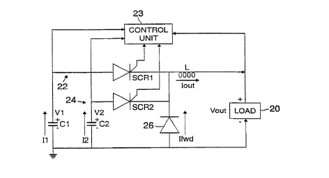
sequential ~;C~-h~ge circuit 10 shown in Fig. 1. Circuit
10 includes two capacitors, C1 and C2, from which power
will be extracted into a load 20 to produce an GuL~L
30 voltage, VOUt. It should be understood that there is an
implied charging system in front of the capacitors. For
example, the capacitors might be the capacitors of a PCS
module that is configured to provide DC step-up or step-
down module, such as is described in U.S. 5,270,913. Or
SUBSTITUTE S~IEET ~ULE 26)
CA 02223679 1997-12-0~
WO 97/01213 PCTAUS96~10740
- 15 -
the capacitors might be the ouL~uL capacitors of a simple
LC charging stage, an example of which will be presented
later (see Fig. 7). In general, the c~p~citors are first
charged during a charging cycle to some predetermined
5 level and then they are sequentially ~;arh~ged into load
20 during a ~is~h~rge cycle.
Circuit 10 includes two ~;C~-h~rge paths 22 and 24,
one connected to capacitor C1 and the other ~o~nected to
capacitor C2. The first ~;Cch~rge path includes a
10 silicon controlled rectifier, SCRl, that is ~on~ected
through inductor L to load 20. The a~o~ discharge path
includes a seco~ silicon ~l.L~olled rectifier, SCR2,
that is also connected through the same inductor L to
load 20. SCR1 and SCR2 are arranged so that when they are
15 triggered on they discharge their respective capacitors
through inductor L. A free wheeling diode 26 is
co~n~cted between ~u.,d and the side of inductor L to
which SCR1 and SCR2 are ~onn~cted Free whe~l ;ng diode
prevents the voltage on either of the capacitors to
20 reversing at the end of a complete ~ia~h~ge. A
le control unit 23 (e.g. a ~_ uLer or general
data processing unit) samples the voltages across the
capacitors Vl and V2, samples the ouL~uL voltage VOUt~ and
triggers the SCR's at the a~ Gp~iate times.
In general, ~iach~ge circuit 10 discharges
capacitors C1 and C2 in sequence and through the shared
~uL~uL inductor L. In addition, for every charge cycle,
there is a discharge cycle in which both capacitors are
typically discharged. The capacitor with the highest
30 voltage is discharged first, followed by the discharge of
the capacitor with the lower voltage. If properly timed,
the excess energy from the high voltage input module
helps to pull out the energy from the low voltage input
module. This method enables input charging to occur at
35 constant intervals and thus it reduces the ~. uLational
SUBSTITUTE SHEET (RULE 26~
CA 02223679 1997-12-0~
W O 97/01213 PCTAUS96/10740
requi~ nts.
As an aside, it should be understood that the term
~load~ when used herein, is meant to have a very general
-~n;ng unless indicated otherwise by the specification
5 or the context in which it is being used. It includes a
node, a power distribution point, a motor, a simple
resistive load, the input of a circuit to which power is
being supplied, etc. In addition, though we have
referred to SCR's in this and subsequent embodiments, any
10 of a wide variety of switching devices can be substituted
for the SCR, depending upon the requirements of the
particular application, including, for example,
thyristors, Crossatrons, GTO's, any semiconductor
unidirectional sWitCh; ng devices, etc.
The following ~;~c~ ion presents the details of a
~s~h~ging cycle that immediately follows a charging
cycle during which capacitors C1 and C2 are charged to
initial voltages of V0l and V02, respectively. For the
following discussion, we assume the ouL~L voltage to be
20 VOUt = 10 kV and an initial voltage condition of V0l >
V02 .
Two different sequential ~ h~ge modes of
operation will be described. In both modes of operation,
it is assumed that the voltage V0l is greater than or
25 equal to twice the ouL~uL voltage VOUt and SCRl is
triggered first to discharge C1 and then SCR2 is triggered
to ~l;~hArge C2. The requirement that V0l 2 Vout iS
n~C~cC~y in order to assure that Cl will completely
~;~ch~ge during its discharge cycle. In the following
30 example, we select V0l = 25 kV which meets this
requirement. The difference between the two modes is in
the timing of the triggering of SCR2. In the first mode,
SCR2 is triggered when V1 reaches zero volts. In the
~qco~ mode, SCR2 is triggered when Vl reaches the value
35 of V02
~STITUrE $~1F~ E 2
CA 02223679 1997-12-05
WO 97/01213 PCT~US96~10740
-- 17 --
When SCR1 is triggered, capacitor C~ h~rges
through inductor L into o~L~L load 20. At the end of
~h~rge (i.e., when vl equal zero), free wheel ~ng diode
J 26 prevents the voltage on C1 from reversing and it
5 permits the energy rem~ini n~ in the inductor L to be
transferred to ouL~L load 20. At the point that Vl
r~h~s zero, the current in the inductor is given by:
(V0l - 2Xvolxvout)
I~ = tL/C1)
and at that point the energy stored in the inductor L is:
EL = 2 XC1X(VO12 - 2XVolXVout)
If we trigger SCR2 when Vl r~Ac-h~s 0 and connect
capacitor C2 through inductor L to ouL~L load 20, the
current in the inductor, IoUt~ represents an initial
condition for the ~;c~-h~rge of the ~con~ capacitor C2.
15 Thus, there will be a certain range of voltages V2 < 2Vout
for which it will be possible to fully ~ hArge the
c~r~s;tor C2. If V02 2 2Vout~ then sequential ~ h~rge
is not required, since the voltage on C2 is sufficiently
large to enable the capacitor to completely ~;sch~rge by
20 itself. However, sequential ~i~h~rging may still be
used in this case in order to combine the effect of the
~Yc~cc voltage of Cl and C2 to aid in ~l;s-h~rging
additional capacitors that have lower voltage levels.
The range of voltages less than 2Vout for which
25 this is true can be solved either analytically,
graphically, or with the use of circuit ~1; ng codes.
If we plot the voltage and current for a ~ h~rge with a
capacitor voltage equal to twice that of the ouL~L
voltage, both the voltage and current will be zero at the
30 end of the ~;~h~rge. If we look at the curve, we will
find that for any current that is less than the maximum
current of:
SUBSTITUTE SHrE~ L~
CA 02223679 1997-12-0~
W O 97/01213 PCT~US96/10740
- 18 -
~ x V ( Cl ) 2
the capacitor voltage V2 has two solutions. The two
solutions correspond to the initial voltages that
capacitor C2 must have in order to fully ~l;cchArge all of
5 the energy from capacitor C2. If the initial voltage of
C2 is between those two solutions, the capacitor cannot
be completely ~i-c~-h~ged. If current remains in inductor
L when V2 reaches zero, an additional capacitor, such as
the input from a third phase, can then be discharged.
As should be readily apparent, the energy and
voltage in each capacitor varies throughout the 60 Hz
cycle if the capacitors are charged from the AC grid.
However, what may not be so apparent is that the total
energy of all of the capacitors is constant and that this
15 is true for any number of capacitors charged from a
multi-phase power source with any number of phases larger
than one. This fact has a very important implication.
It does not matter when in the 60 Hz cycle the ~;cch~rge
is begun since the total energy in all of the capacitors
20 remains constant throughout the cycle. Thus, there will
be a constant power flow through the circuit so long as
the capacitors are completely ~i-c~h~ged and they are
originally charged at constant time intervals.
The complete ~ h~rge of Cl and C2 is possible
25 only if their initial conditions are properly selected.
V0l must be at least 2Vout to enable it to fully ~icch~ge
into a node that is at VOUt. Even if V0l is above 2Vout,
if it is not sufficiently above 2Vout, the residual
current that ~~ ~i nC in inductor L when Vl reaches zero
30 may not be sufficient to cause the complete ~icch~rge of
C2 into the node at VOUt. Fig. 2 presents a plot of the
different operating regions of the circuit shown in Fig.
1. The x-axis represents the ratio of the initial
voltage across Cl to the vuL~uL voltage (i.e., Vol/VOUt);
SvBsTlTuTE SHEET (RULE ~6)
CA 02223679 1997-12-0~
WO 97101213 PCT~lJS96~10740
and the y-axis r e~_ents the ratio of the initial
~ voltage across C2 to the ouL~uL voltage (i.e., V02/VOut).
If the initial voltages on capacitors C1 and C2
are properly selected, both capacitors can be fully
5 discharged at the end of a sequential discharge cycle,
with no residual current remaining in inductor L. The
set of conditions which produce such a result are shown
by curve 30. The e~uatio~ for curve 30 is as follows:
V02 = Vout+ (Vou~2- Vol2+2xvOuexvol)l/2
10 The condition can be put in a simpler form:
El+E2 = 2x(E1l/2~E21/2)
where Em is the ratio of ~he initial energy stored in
capacitor Cm divided by the energy r ~ ~; n i~g when its
voltage equals the ou~uL voltage, V0ut. If the condition
15 is such that the left side of the e~uation is smaller
than the right side, then the initial condition falls to
the left of the curve in the Fig. 2 and the second
capacitor cannot be ~;sch~ged.
If the initial conditions fall within the region
20 to the left of curve 30 but to the right of Vol/VOut =
2.0, then it will be possible to fully discharge
capacitor C1 but not capacitor C2. In the region to the
left of the line Vol/VoUt=2.0, it will not be possible to
fully discharge either C1 or C2.
If initial conditions fall within the region to
the right of curve 30, then both capacitors can be fully
discharged through sequential discharging with some
residual current rem~; n; ng in inductor L. As noted
above, the residual ~ Le~l~ in inductor ~ can supply the
30 initial condition for discharging a third capacitor (not
shown), where the combined condition of the first two
capacitors, if a~- ~r iately selected, will permit the
full ~is~hA~ge of the third capacitor. Following the
above reA ~on; ng, it should be apparent that the solution
SUBSTITUTE SHEET (~E ~)
CA 02223679 l997-l2-0~
W O 97/01213 PCT~US96/10740
- 20 -
for V03 (i.e., the voltage(s) at which full ~i~h~ge is
possible) will have four roots or, once the voltage for
the first two capacitors is specified, two roots. This
process can be cont;nl~e~ as long as a residual inductor
5 current remains on subsequent ~;s~h~rges. The ~iR~rge
sequence is best performed with the discharge of
capacitors in the order of decreasing voltages.
Figs. 3A and 3B show simulated G~L~uL ~u. e~lL and
voltage waveforms, respectively, for one complete
10 ~ hA~ge cycle of operation of the above-described
sequential ~;~h~rge tech~;~ue. In this example, SCRl is
triggered first and when Vl reaches zero volts, SCR2 is
triggered. The initial voltage V0l was selected to be 25
kV and V02 is some smaller value, as ; n~ i r~ted on the
15 curves. By selecting V0l to be 2.5 times the o~L~uL
voltage VOUt~ this permits the full discharge of C2 over
the complete range of initial voltages that C2 might
have. If the voltage V0l is between 25 kV and 20 kV, the
voltage range for V02 which will allow full ~;~ch~ge is
20 restricted in the ~nner which will be described below.
For the numerical calculations that were performed, the
capacitors all had values of 1 ~F and the inductors all
had values of 6.338 mH. In Figs. 2A and 2B, the family
of curves represent the different values of V02, i.e., the
25 initial voltage across C2.
As indicated in Fig. 3A, the o~L~uL current IoUt
through inductor L is relatively large at the time that
Vl reaches zero volts and SCR2 is triggered on. This
residual current helps to completely pull out the charge
that is stored in c2. As indicated in Fig. 3B, the
voltage across C2 remains at V02 until SCR2 is triggered
on and then C2 fully discharges to zero volts. It should
be apparent that in all cases there is a residual ~Ul' ellL
remaining in Lout at the point that C2 is fully
35 ~ h~ged In this case, free wheeling diode 26
SUBSTITUTE SHEET (RULE 26~
CA 02223679 1997-12-05
WO ~7/~2~13 PCT/US96~10740
-- 21 --
provides a bypass path for the residual current in
inductor L allowing the inductor to completely ~ hArge
ana preventing its residual current from reversing the
voltage on any of the capacitors. As noted earlier, the
5 residual current could instead be used to ~ hA~ge yet
another capacitor if there were more input stages in the
circuit.
As noted earlier, sequential ~ischA~ge may also be
performed in a Qec~ mode. Instead of triggering the
10 ~ecQn~ ~i~ch~ge at the point when the voltage of Cl is
zero, one may trigger it at the point when v1 r~he~ V02,
the initial voltage of the second capacitor. By
triggering at this point, both capacitors are effectively
connected in parallel and are being ~i~h~rged together.
15 The current and voltage waveform for this type of
~;~h~ge sequence are shown in Figs. 4A and 4B,
respectively.
Both sequential ~i~chArge modes of operation yield
about the same ~ hA~ge periods and require similar
20 ~- -l,ents. The first approach (i.e., triggering SCR2
when V1 rPAch~ zero) has the advantage that correct
timing of the s~conA phase of discharging is easier to
accomplish. From an operational point of view, the
QeCO~ approach (i.e., triggering SCR2 when V1 reaches
25 V02) is more difficult to implement. In the second mode
of operation, if the timing of the start of the ~i~chA~ge
of the second phase is not accurate, the first capacitor
will not be fully ~ic~-h~rged.
Seouential Dischar~e Rectification (SDR)
To summarize what was presented above, the
seauential discharge rectification technique involves
i ~hA~ging ; n seauence all input modules (e.g.
capacitors or PCS modules) through a shared o~u~
inductor using a shared free-w~Pel ;ng diode. In
SUBSTITUTE SHEET (RULE ~6)
CA 02223679 1997-12-0~
W O97/01213 PCT~US96/10740
- 22 -
addition, the modules are ~;~ch~ged in decreasing order
of the initial module voltage. The ~YC~s~ energy
remaining in the vuL~uL inductor from the discharge of
the first module helps "pull out" energy from the
5 capacitors of the ~CQ~ and third modules, which have
lower voltage levels.
An ouL~L section for three phase rectification
circuit is shown in Fig. 5. One SCR per phase (i.e.,
(SCRl SCR2, and SCR3) r~ hArges a correspon~;n~
10 capacitor (Cph1, Cph2, and Cph3) into a shared output
inductor Lout~ which is, in turn, conn~cted through a
filter section 27 to a load 30. Filter section 27
filters out any ripples that are caused by the pulsed
~i~ch~ge of the capacitors into the load.
The components of a low-pass ~uL~uL filter are
also shown in Fig. 5 in the fl;~Ch~ box. Note that the
illustrated filter design is very simple, consisting only
of three reactive elements: Lf, Cfl and Cf2, conn~cted as
shown. Since the energy is dumped into Cf1, its
20 capacitance should by at least about 3-5 times larger
than the capacitance of the storage capacitors, Cphi. By
selecting a filter cut-off point that is lower than the
lowest expected repetition rate of the circuit, a smooth
GuL~uL voltage is pro~t~c~A. The filter can, of course,
25 be of any a~~ iate design which is capable of
eliminating the ripple that the sequential ~ hA~ge
tends to introduce.
As noted previously, the shared ~uL~uL inductor is
a key _ _sn~nt for the sequential ~;~h~ge operation
30 since it allows any residual current ,. ~;n;n~ from the
~;~h~ge of one capacitor to assist in achieving the
complete discharge of another capacitor.
apacitors, Cph1~ Cph2~ and Cph3, each represent a
different capacitor (in this case, ~stack of capacitors~)
35 within a correspon~;ng PCS module (not shown). Each PCS
SUBSTITUTE SHEET (R'l5LE ~6)
CA 02223679 1997-12-05
W O 97~01213 PCTAUS96/10740
- 23 -
module is co~nected to a different phase of a three phase
AC line. In other words, each capacitor is charged to a
voltage that is proportional to the absolute voltage of
the ~OL e~l .o~ i n~ AC input phase at that time. It is
5 assumed for ~uL~G~es of this example that the PCS mo~ e~
each provide a step-up factor of N. Thus, the voltages
across each of the capacitors can be dete~ ; n~ as
follows:
VC1 = 2 X ¦A ~in(~ t) ¦ XN
V~ = 2x¦A sin(~ t+2~/3) ¦XN
v~ = 2x¦A sin(~ t-2~/3) ¦XN
where "A" is the AC input voltage amplitude and N is the
step up ratio of the PCS module.
As before, a ~ylammed ~GllL~ol u~it 23 ~n~ols
15 the operation of the charging circuit and the sequential
discharge circuit (e.g. the triggering of the SCR's).
The capacitor voltages ~or the three ph~c~c are
shown in Table I over an angle of 60 degrees (see columns
labeled Phase 1, Phase 2, and Phase 3). The numbers are
20 for an rms input voltage of 11 kV and a step-up ratio of
N=6. Table I has eight entries separated in time by 7.5
electrical degrees.
SIJBSTITUTE SHEET (RULE 26)
CA 02223679 1997-12-05
W O 97/01213 PC~rrUS96/10740
-24-
-w'
N
~ W
--I W ~ ~ ~ ~'7
E ~
o t~) o
~ ~ o
~D O t' In ~ t' O
' ' ' '
,. ~ a~ o o o o o o
S P
Pt
C~ W 0~
~D O O OD ~O ~ O O
0 ~ t~ ~ ~ ~q
d o
P
~ ~ ~ o o ~
O O ~O ~D CO O O ~D
d ~
.C P
~ ~ U7 ~ ~D _I ~ O
0 U ~ ~ ~ ~i
W
E~ ~
U~ O
SUBSTITUTE SHEET ~RULE 26)
CA 02223679 1997-12-0
W O 97~01213 ! P~nuss6/~a
- 25 -
By triggering the charging cycle at the listed times the
~ corr~pon~;ng c~pAc~tor voltages are ob~;n~. Identical
voltage combinations are repeated every 60 degrees with
the cyclic shift of all the columns to the right.
The SCR's are triggered starting with the
capacitor having the highest voltage and procee~ing
seguentially through the rest of the capacitor in order
of decreasing voltage. For each charge cycle, the
discharge sequence is as shown in the last colllmn of
10 Table I. For example, look at the entries in the row at
time 0.174 msec. The charging cycle associated at that
time establi~h~s voltages on Cph1, Cph2, a ph3
8g,618, and 96,657 volts, respectively. Given the
relative ordering of the capacitor voltages, the
15 ~ h~ge will be in the following order: Cph3, Cph2, and
Cphl '
It can be simply shown, either mathematically or
numerically, that the combined energy of the three
capacitors is at all times a constant and is given by:
Et = 1.5x CxN2 (2A)2
The quantity of combined charged energy is
; n~p~n~nt of the phase angle and source frequency. In
other words, the combined energy is identical for each
and every charge cycle. It follows that if one simply
25 charges and discharges these capacitors together at
cc~ rolled time intervals, the input power and c,uL~I_
power can be independent in time and no synchronization
with the AC cycle is required.
Also, by charging each capacitor at constant time
30 intervals, the energy extracted from each line is
~' V~UL Lional to the square of the instantaneous voltage.
This is exactly what the power flow is into a resistive
load. It therefore follows that by using this power
extraction method, the power factor of the AC input is
SUBSTITUTE SHEET (RULE 26)
CA 02223679 1997-12-0~
W O 97/01213 PCTAUS96/10740
- 26 -
identical to unity and no reactive power flow occurs.
Control circuit 23 monitors the load and sets the
repetition rate based upon the required th~ou~l,puL that
is demanded by the load. If the load or the input
5 voltage changes, a simple feedback loop can adjust the
frequency at which the charging/discharging cycles occur
to maintain a constant ouL~u~ voltage.
Figs. 6A and 6B show, respectively, the input
voltage waveform 40 and the input current waveform 42
10 over 60 degrees of a 60 Hz three-phase input, with the
capacitors charged to the voltage levels listed in Table
II. (Note that in this case ~input~ refers to the input
of the ouL~u- filter 27.) As can be seen, the input
condition of the c~co~ 30 degrees is the image of the
15 first 30 degrees. In addition, the input condition is
repeated every 60 degrees. Fig. 6A presents the
capacitor voltage of the switched on capacitors and the
inductor ~Ul ' ~1~. As can be seen from the current
~continuities~ the inductor current is substantial by
20 the time the ~eco~~ and third capacitors are switched on
line. In addition, the inductor and free-wheeling diode
current do not have to be zero between consecutive
capacitor ~i~ch~rge cycles.
In Figs. 6A and 6B, the charging of the three
25 capacitors occurs at the same time. It is assumed that
the charging time required to charge each of the
capacitors through a corresponding input inductor (not
shown) takes about 250 ~sec. This determines how
frequently the capacitors can be charged and how soon one
30 ~ic~hArge cycle can follow a previous ~ h~rge cycle.
It should be noted that to generate the waveforms that
are shown, in particular, the repetition frequency of the
~1~h~ge cycle, there is implied (but not shown for
purposes of simplifying the circuit) a second set
35 charging and discharging circuits, including three
SUBSTITUTE SHEEl (RULE 26)
CA 02223679 1997-12-0~
W0 97/01213 PCT/~JS96~0740
-- 27 --
additional capacitors. The second set of circuits is
- coupled into the circuit shown in Fig. 5 in parallel with
the illustrated set of discharging circuits. Each of the
capacitors in the other charging/~;schArging circuits is
5 coupled to shared inductor Lout through a ~r r e~ollding
SCR. While the ~irst set of capacitors ( i . e ., Cphl , Cph2 ,
and Cph3) is being discharged, the second set of
capacitors (not shown) is being charged. In this way,
there will always be a set of capacitors that is
10 immediately available for the next discharge cycle
without having to wait for a charging cycle to be
performed. Thus, the circuit can be operated at a higher
repetition rate.
Figs. 6A and 6B also show the low pass ~L~uL
15 filter voltage 46 and o~L~uL c~,-ellL 48. Of prime
importance is that both the o~L~L current and o~L~uL
voltage are constant. Not shown, but of equal
importance, is that both the input voltage and input
current of all three phases is sinusoidal and ripple-free
20 even with the use o~ small low-pass input filters.
Note that as the repetition rate increases so does
the ripple frequency. If the low-pass ~uL~uL filter
section is designed to handle the lowest repetition rate
that is anticipated for the system, it will then handle
25 the higher ripple frequencies that are pro~llce~ at faster
repetition rates.
If thyristors are used for the SCR's, they should
have a rapid recovery rate, i.e., a short tQ. Since the
discharge is completed within about 250 ~sec, the SCR's
30 will see forward bias in about 125 ~sec. They need to be
recovered before they experience the forward voltage.
Thyristors having the required recovery are available
commercially.
For the conditions described above, the o~L~L
35 capacitor values are 9.1 nF, the load is 7 kn for a total
SUBSTITUTE ~HEET (RULE 26)
CA 02223679 1997-12-0~
W O 97/01213 PCT~US96/10740
- 28 -
power throughput of 225 kW. A much higher throughput can
be obtained by using a single string of st~n~rd and
unparalleled high voltage thyristors for the SCR's.
Using typical 8 kA thyristors, an ouL~u~ power of over
5 200 MW can be obtAinP~ with one set of three modules.
The same t~chn i~ue can be used in the lower or consumer
voltage range. In this regime faster and lower voltage
switching devices can be used with a higher switch; nq
speed and lower forward voltage drop. This will lead to
10 a more optimized throughput and higher efficiency.
Alternative SDR Configurations:
For rectification applications, the capacitor
voltages must always be the same polarity as the o~L~L
voltage to transfer power out of the system into the
15 load. Since the input voltage to the charging circuit is
negative over half of the input waveform cycle, this
portion of the waveform cannot be used. This problem can
be solved in at least two ways. One approach is to allow
the input capacitors to charge to a negative voltage and
20 then use an inversion cycle to flip the voltage to a
positive value. The inclusion of the inversion cycle in
this later approach r~ c~ the ~Y; repetition rate
that is achievable with the system. Another approach is
to generate six ph~e~, Thus, there will always be input
25 waveforms having positive polarity throughout the entire
cycle. Examples of these two approaches are described
below.
An alternative three phase rectification circuit
without transformation (i.e., without using the PCS
30 module for transforming the input waveform) is shown in
Fig. 7. The three phases of the AC input line are
represented by the inp~ts labeled Phase 1, Phase 2, and
Phase 3. The circuit includes three charging circuits
60(1-3), one for each phase, for charging a corresponding
SUBSTITUTE SHEET (RULE 26)
_
CA 02223679 1997-12-0
WO 97/01213 PCTJUS96J2 1~74
-- 29 --
one of three capacitors, Cl, C2, and C3. The charging
circuit for C1 includes an input filter section 70(1), a
pair of SCR's (i.e., SCRinl+ and SCRinl_) and an input
inductor, Lin1~ SCRinl+ is for charging C1 from the
5 positive polarity portion of the AC input waveform and
SCRin1_ is ~or charging C1 from the negative polarity
portion of the AC input waveform. The charging circuits
for the other two capacitors (i.e., C2 and C3) are
constructed identically to the first charging circuit and
10 thus their corresponding components are similarly
labeled.
Each capacitor is resonantly charged through its
input inductor from the input phase to which it is
conn~cted. For example, Cl is resonantly charged through
15 LLnl from phase 1, and similarly for the other capacitors.
Thus, the charging period is detel ; n~ by the selection
of the value of the input inductor.
On a three phase line, at any given time there
will be either one or two phA~c which have negative
20 polarity. Thus, the corresps~; nq capacitor(s) will be
r~o~Antly charged to a negative voltage. An inversion
circuit co~nected across the capacitor invert the
negative voltage after the charging cycle is complete and
prior to the discharge cycle. In the case of capacitor
25 C1, the inversion circuit includes an inductor Li1 and
silicon ~on~rolled rectifier SCRil. Similar inversion
circuits are connected across the other capacitors C2 and
C3. With the inverting circuits, all three capacitors
can be made positive prior to the ~;C~h~rge cycle even
30 though they were charged from a negative portion of the
input waveform. This simply requires the inclusion of an
inverting cycle between the charging cycle and the
discharging cycle. Thus, all three phases can contribute
to every ~ic~h~rging cycle.
In this rectification circuit of Fig. 7, the
SUBSTITUTE SHEET (P~ULE 26)
CA 02223679 1997-12-0~
W O 97101213 PCT~US96tlO740
- 30 -
discharge circuits are constructed basically as
previously described. Each capacitor C1, C2, and C3, is
co~nected through a correspo~nq one of SCR's (i.e.,
SCRoil, SCRoi2~ and SCRoi3) into a shared ou~u~ inductor
5 LoUt~ The other side of Lout is conn~cted through an
vuL~uL ripple filter to a load 62 (e.g. power
distribution node). A co~ ol unit (not shown) ~~ ols
the triggering of the SCR's to produce the charging,
inversion, and ~ hA~ging cycles of operation.
If a six-phase source is available, the inversion
components and the inversion cycle can be eliminated, as
shown in Fig. 8. The circuit is the same as that shown
in Fig. 7 except that each capacitor can be charged from
two ph~ce~ of the six phase source. Thus, for example,
15 capacitor Cl, which is resonantly charged through Lin1, is
cQnn~cted to Phase 1 through SCRinl and to Phase 4 through
SCRin4. The two phA~e~ from which C1 is charged are
selected to be 180~ out of phase with each other so that
when the voltage of one waveform is negative the voltage
20 of the other waveform is positive. The charging of each
of the other capacitors C2 and C3. Thus, at all times
throughout the AC cycle, each capacitor can be charged
from a positive voltage source. With this arrangement,
the inverting circuit are not needed; instead, the
25 triggering of the SCR's is controlled to correctly select
that Phase from which power will be extract during each
charging cycle.
The configuration of Fig. 8 provides each input
phase with the correct polarity, requires no inversion,
30 and permits a 50% higher throughput than for the three-
phase throughput. This configuration can be further
exploited by adding a seco~ rectification circuit of
identical design to generate both a positive and a
negative DC ouL~L polarity.
For large power systems, the six phases can be
SUBSTITUTE SHEET (RULE 26)
CA 02223679 1997-12-0~
WO 97~01213 PCT~lJS9C~10740
generated simply by using two sets of transformers with
half of full ratio. A three phase system can be easily
converted to a six phase system with the use of center-
tapped transformers, such as are shown in Fig. 9. The
5 center tap of the s~con~A~y is the neutral line and the
outside lines of the s~con~ry furnish the two ph~Pc,
one being the inverse of the other.
The six-phase rectification and step-up may also
be attractive with transformation. The complexity of the
10 transformation modules can be reduced ~epe~ing on power
throughput. In addition, efficiency can be increased and
triggering re~uirements r~A~ , since several diodes can
be used in place of SCRs.
Another beneficial configuration is rectification
15 of a six-phase power source generating a plus and minus
DC ouL~L source. The six phases may be made available
with small modifications of generators by bringing out
three additional phases from the generator w; n~; n~,
Using the typical ouL~uL of 10 kV a one-step
20 rectification and step-up to a voltage range of +40 to
+120 kV can be o~tained with a power level in excess of
100 MW.
Control Module:
The interpulse separation sets the ou~uL voltage
25 to the desired level. The algorithm for co..L~olling the
interpulse separation or repetition rate of the
charging/discharging cycles is straight forward. Note
that the same amount of energy is taken in per pulse of
operation. Thus, the power throughput of the system is
30 proportional to A2 x (repetition rate). If the input
voltage drops by 10%, the power throughput will drop by
about 20%. To compensate for the 10% drop in input
voltage, the repetition rate must be increased by about
20%. Similarly, if the ouL~uL power drops by 10% (e.g.
SUBSTITUTE SHEET (F~IJLE 26)
CA 02223679 1997-12-0~
W O 97/01213 PCTrUS96/10740
- 32 -
because loading is less), then to compensate, the
repetition rate must be decreased by 10~. If the
repetition rate is not decreased, the ~uL~uL voltage will
rise.
By measuring the input voltage, the G~L~uL
voltage, and the ouL~uL current, one has all of the
information that is required to control the operation of
the system.
To accurately set the firing sequence, it is
10 n~c~fi~Ary to know where you are within the cycle of the
input waveform. This can easily be dete~ ;n~ by
locating the zero crossings of the waveform. one
approach to detecting the precise time at which zero
crossings occur is to use a small transformer with an
15 easily saturated iron core. Referring to Fig. lOA, such
the primary of such a transformer 80 is co~n~cted between
the phase line and ground with an a~ iately large
resistor limiting the current through the primary.
Throughout most of the AC cycle on the phase 1 line, the
core will r~~ saturated, except for a very short
period when the voltage waveform crosses zero. While the
core is saturated, the ouL~uL voltage on the ~co~ry
will be zero. When the core comes out of saturation at
the zero crossing, a pulse or blip will appear on the
25 secondary marking the precise location of the zero
crossing, as illustrated in Fig. lOB.
Rectif;cation with Step-down Transformation
The conversion of power from AC to DC is typically
~c~ _lished using a rectification bridge in concert with
30 other active and discrete components. The most common
bridge configurations are half-wave, full-wave and six-
phase, with the latter producing the most refined ouL~uL
voltage. Less common is the twelve-phase configuration,
which can be accomplished by placing two six-phase
SUBSTITUTE SI~EET (RULE 2~)
CA 02223679 1997-12-0~
WO 97~0~Z~3 PCT~US96~10740
rectifiers in series. The twelve-phase system minimizes
ouL~uL voltage ripple by increasing the fre~uency at
which power is delivered to the load. In high current
applications where the ouL~uL voltage is relatively low
(<50v), half-wave rectification is used because the
inherent losses are lower.
The above-descri~ed SDR systems are regulated high
power AC to DC converters. The relatively high operating
frequency and continuous power transfer produce a ripple-
10 free uuL~L voltage that can be effectively regulated byvarying the rate of conversion. The conversion process
continuously draws current from the source thereby
eliminating reactive power generation.
However, the SDR systems depicted in Figs. 5, 7
15 and 8, have losses that are even higher than those found
in a full-wave bridge rectifier. As in the full-wave
bridge rectifier, the above-described SDR systems also
use two solid state devices (i.e., SCR's) in series: one
for the r~o~nt charge cycle and the second for the
20 ~ hArge cycle. Unfortunately, the SCR's, which are
typically multijunction devices, have much larger forward
voltage drops than the single junction diodes that are
used in the conventional full-wave bridge rectifier (e.g.
2 volts versus 0.7 volts). In low voltage applications
25 where the ratio of the operating voltage to the SCR
forward voltage drop to (Vo/Vf) is small, the losses can
become significant. In applications such as aluminum
production, electro-plating or copper refinement where
high currents at voltages less than 50v are required,
30 thus a modified SDR configuration would be more suitable
to reduce the impact of the losses on system efficiency.
In general, the modified SDR system includes a
front end which performs the sequential ~ hA~ge
functions at high voltage levels and it includes an
35 ouL~L stage which uses a small, high frequency
SUBSTITUTE S~EET (RIJLE 26)
CA 02223679 1997-12-0~
W O 97/01213 PCT~US96/10740
transformer to step down the voltage to the re~uired low
voltage level. This greatly improves the overall system
efficiency by increasing the Vo/Vf ratio of the sequential
~ h~ge section of the circuit. The modified SDR
5 system has an efficiency similar to that of the s~n~rd
half-wave rectifier while eliminating the need for an AC
power transformer. The front end which performs the
sequential discharge appears as a resistive load to the
grid. Thus, it exhibits of the previously described
10 benefits of SDR including harmonic free rectification and
producing a power flow of unity power factor.
An illustrative configuration is shown in Fig. 11.
As before, there are three capacitors, Cl, C2, and C3,
each of which is charged from some power source, e.g. a
15 three phase line (not shown). The charging circuit for
each capacitor might be a corresponding different PCS
module or it might be a simple reCo~nt charging circuit,
such as is illustrated in Fig. 8. In the latter case,
each capacitor Cl, C2 and C3 is resonantly charged by an
20 SCR and inductor in series. The resulting voltage on
each capacitor will be twice the instantaneous voltage of
input line and it will have the same polarity as that
instantaneous line voltage. When the resonant charging
is complete, the capacitors are sequentially ~;~h~rged
25 in order of their absolute voltage levels, as has been
described previously.
In the circuit of Fig. 11, the capacitors are
~;~çh~rged through a coupling pulse transformer 100 into
a shared ouL~uL inductor, Lout~ Transformer 100 has two
30 primaries 102(a) and 102(b) and it has two s~con~ries
104(a) and 104(b). Each of the dual secondaries 104(a)
and 104(b) is connected to inductor Lout through a
corresponding one of two ouL~L diodes Da and Db, which
select the positive voltage output polarity. The rest of
35 the o~L~uL section is as previously described. It
SUBSTITUTE S~EFI (RULE 26)
CA 02223679 1997-12-0~
W O 97/012~3 PC~AUS96~0740
- 35 -
includes a free-wheel;ng diode DfW and a low pass ouL~L
~ filter section including Lfilter, cf1~ and Cf2. Free
wh~el;~ diode DfW assures that any energy ~ in~ in
the ouL~uL inductor Lout is transferred to the load
5 following the last capacitor ~;~chA~ge and it also
prevents the voltages across the capacitors from
reversing after they are discharged to zero volts during
the ~;~hA~ging cycle.
An array of SCR's coupling the capacitors to the
10 transformer 100 steer the discharge of each capacitor to
the appropriate one of the two primaries 102(a) and
102(b) of transformer 100, depending upon the polarity o~
the voltage on the capacitor that is being discharged and
d~p~n~;ng upon the direction of the magnetic flux within
15 the core of transformer 100 from a prece~ing discharge
cycle. Four SCR's (namely, SCRla+, SCR1a_, SCRlb+, and
SCRlb_) provide separate ~;C~hArge paths from capacitor C
to trans~ormer 100. SCRla+ iS used to ~ hAl-ge a
positively charged Cl through primary 102(a); SCRlb~ is
20 used to ~i~chArge a positively charged C1 through primary
102(b); SCRla_ is used to discharge a negatively charged
Cl through primary 102(a); and SCR1b_ is used to discharge
a negatively charged Cl through primary 102(b). A
correspo~;ng set of SCR's, which are labeled in a
25 similar manner, are used steer the discharge of
capacitors C2 and C3.
A control module (not shown, but previously
described) establishes the triggering sequence which
assures proper transformer flux reversal from one
30 ~;~hArge cycle to the next. The circuit of Fig. 11
permits the use of three-phase input power directly, and
eliminates the need for both a AC step-down transformer
and a polarity inverting transformer.
Note that the use of the dual primary - dual
35 seco~Ary transformer allows one to reverse the magnetic
SUBSTITUTE SHEET (RULE 26)
CA 02223679 1997-12-05
W O 97/01213 PCTrUS96/10740
- 36 -
flux in the core from one triggering sequence to the
next. This means that an even smaller transformer can be
used without fear of saturating its core during
operation.
An example of a triggering sequence will now be
presented in detail to further illustrate the operation
of the circuit shown in Fig. 11. Assume, for purposes of
this example, that the three capacitors C1, C2 and C3 are
being charged from a three-phase 440 V, 60 Hz AC line and
10 that the trigger rate is 48 times per cycle or 2,880
times per ~eco~. The voltage on each capacitor at the
end of each charging cycle can be determined by the
following equations:
Vcl=2xA sin(~t)
Vc2=2xA sin(~t+2~/3)
Vc3=2xA sin(~t-2~/3)
where "A" i5 the AC input voltage amplitude of 392 volts.
Table II shows capacitor voltages vs. time and it
presents the triggering sequence over an angle of 60
20 degrees. The table has eight entries separated in time
by 7.5 electrical degrees, or every 0.347 msec. The
capacitor charge voltage and polarity is shown in columns
2 through 4. Column 5 shows the capacitor ~;~ch~rge
sequence, and column 6 shows the SCR triggering sequence.
SUBSTITUTE SHEET (RULE ~)
CA 02223679 l997-l2-05
W O 97/01213 PCTAUS96~0740
- 37 -
~D+++++++~
U 'I '~ '~ --I
.,. ~,,~________
b'~________
o q) -- ~ ~ ~ ~ _ _ _
~ U ~ ~ ~ ~ ~1 ~1 ~1 ~1
~________
U ~ ~7 ~ ~ ~ ~ ~ ~ r~
d
O CO
o ~ a~ ~ ~ c~ ~ ~1
,~ . . . . . . .
O ~ ~ r o
I
o
.~,co~a~U7t~ o o ~r~
,.~. . . . . .
U o~
p ~o _I ~ ~ ~ ~~ _I 00 ~
.
o o O ~
U~ o
_I
SUBSTITUTE SHEET (RULE 26)
CA 02223679 1997-12-0~
W O 97/01213 PCTAUS96/10740
- 38 -
To understand how to interpret Table II, look at
the first row where time equals 0.174 msec. A charging
cycle o~u~ling at this point in the input voltage cycle,
charges each of the capacitors to the voltages shown in
5 the columns labeled Vcl, Vc2, and Vc3~ Thus, at the end
of the first charging cycle, the voltages on C1, C2, and
C3 are +51.3, +651. 8, and -703.0, respectively. Since
the magnitude of the voltage on C3 is largest and the
magnitude of the voltage on Cl is smallest, the ~i~ch~ge
10 sequence will be 3-2-1, as indicated in the column which
i8 entitled 'ICapacitor SequenceJ. Since C3 is charged to
a negative voltage, either SCR3a_ or SCR3b_ must be used
to ~i~h~ge it through coupling transformer 100. In
this case, the choice was SCR3b-, as indicated in the
15 column entitled ~Triggering Sequence~. once the voltage
across Cl reaches zero volts, C2 is discharged through
SCR2a+, followed by the discharge of Cl through SCRla+.
Notice that the SCR's that are selected to steer the
~ifich~ge are selected to keep the magnetic flux in the
20 transformer core going in the same direction throughout
the entire discharge sequence.
At the end of the ~ hA~ge sequence the voltages
on the capacitors will be zero. During the next charging
cycle, which oc~u - at T=0.521 msec, the capacitors will
25 be charged to the voltages shown in the second row of
Table II. Since C3 again has the largest voltage and Cl
the smallest, the ~ifichA~ge sequence will be the same as
before, namely, 3-2-1. This time, however, the SCR's are
selected so as to reverse the magnetic flux in the
30 transformer core as ~ _A~ed to the previous discharge
cycle. Thus, to ~isch~rge Cl instead of triggering SCR3b,
the control module triggers SCR3a_. When Vcl reaches
zero, SCR2b+ is triggered to ~i~hA~ge C2 and then SCRlb+
is triggered to discharge C1.
By adding a c~con~ bank of capacitors as shown in
SUBSTITUTE SHEET (PLU~ 26~
CA 02223679 1997-12-0~
WO 97/0~213 PCT/US96/1~740
-- 39 --
the dual input configuration shown in Fig. 12, we can
effectively double the power throughput of the system.
In this configuration, there are two banks of capacitors,
an upper bank labeled "a" and a lower bank labeled "b".
5 The upper bank includes capacitors C1~, C2a, and C3a, each
of which is charged from a different phase of a three
phase input grid. The lower bank includes capacitors Clb,
C2b, and C3b, each of which is also charged from a
different phase of a three phase input grid. The
10 capacitors are grouped in pairs (e.g. C1a and Clb), each
pair being charged from the same phase of the input grid.
As one capacitor of a pair is being charged, the other
capacitor of that pair is being discharged.
Each of the capacitors in the upper bank is
15 conn~cted to an upper primary 102(a) of coupling
transformer lOo through two SCR's that are arranged in
parallel but with their polarities reversed with respect
to each other. For example, Cla is co~nected to upper
primary 102(a) through SCRla+ which when triggered allows
20 current to flow from capacitor C1a to upper primary
102(a), and through SCRla_ which when triggered allows
current to flow from upper primary 102(a) to capacitor
C1a. SCR1a+ is used to discharge capacitor C1a when its
voltage is positive and SCRla_ iS used to ~ ~hAl~ge
25 capacitor C1a when its voltage is negative. The discharge
circuits for capacitors C2a and C3a are arranged similarly
and thus the correspo~; ng components in Fig. 12 are
labeled in like fashion.
Similarly, each of the capacitors in the lower
30 bank is conn~cted to a lower primary 102(b) of coupling
transformer 100 through two SCR's that are arranged in
parallel but with their polarities reversed with respect
to each other.
This circuit configuration greatly improves the
3S utilization of the thyristors by allowing the first set
SUBSTmlTE SHEET (RIJLE 2~)
CA 02223679 1997-12-0~
W O 97/01213 PCT~US96/10740
- 40 -
of capacitors to be charged from the input grid during
the ~i~h~ge cycle of the second set. It also allows
the operating frequency to be about twice that of the
configuration of Fig. 11. If the operating frequency is
5 doubled, this r~ the filter requirements and l~c~n~
the total cost per unit power throughput.
In the dual input configuration, each pair of
capacitors (e.g. Cla and Clb) shares an input filter, and
all capacitors may share an GuL~L transformer, ouL~L
10 diodes and the ~uL~uL filter. Thus, this configuration
also has the effect of lowering the overall system cost.
The doubled operation is shown in Table III. As
can be seen, the charging rate and power throughput has
been increased by a factor of two. The charging and
15 discharging sequence is identical to than of Table II,
except that the rate has been increased.
Si.lB~TlTUTE SHEET (RULE 26)
=
CA 02223679 l997-l2-05
W O 97/01213 PC~USg6~10740
- 41 -
-~ o ~ N N N N ~ N N +
~1~S+ + + + + + + + + + + + + + + t~
R ~ R ~ ~ ~ ~ ~ ~ ~ ~ ~ ~ ~
N N _ N N N N N ~1 ~1 ~ I +
~ Q ~ ~ ~ Q ~ ~ ~ Q ~ ~ ~ Q
~~1 d ~ ~ R ~ .4 a~
H
HH
m ~ ~ . . . . . . . . . . . . . .
E~ -- O O ~ ~ ~ ~ ~ D U) ~ ~ O
I
~1~ 0 a~ ~ ~7 ~ ~ ~ o 1~ o o ~ o ~ ~r~
U--0~ O ~ ~ ~~
~n ~ oo ~ _I t~ ~ a~ ~ o ~ o u~ ~ Ir. ~
U--ol ~ O ~D ,i In ~ ~ d' O~ _i _~ co
P p ~r~ ~ ~ ~ ~ O ~ a.
,. ~ ~ O O O O O _i _i _i _i ,i _i
~ o In
SUBSTITUTE SHEET (RULE 26)
CA 02223679 1997-12-0~
W O 97/01213 PCTAUS96/10740
- 42 -
Notice that in Table III the time steps have been
re~llc~ and there is reference to capacitor banks a and b
(for the upper or lower capacitors, respectively).
The trigger t; ;ng of the second and third ~uL~L
5 SCR's, in the sequence shown in Table III, is such that
no energy ~ -; nC in the capacitors and no free-wheeling
current flows until the last capacitor is discharged.
During normal operation, the maximum free-wh~el;ng
current is only a fraction of the total ouL~uL current.
10 The free-wh~l ;ng diode's function is not only to
facilitate the full capacitor energy transfer but also to
permit ouL~uL voltage regulation.
The losses in the output diode of a st~n~d half-
wave rectification system are identical to those in the
15 free-wheeling diode in a SDR system. For low ouL~uL
voltage systems the dominating losses occur in the ~L~L
diodes. In either configuration, the total ou~L
current has to flow through one of the two diodes. The
SDR system ove~c~ -- the inherently greater losses by
20 operating at a higher voltage, thus ;n; ; zing the
current through the switches. The losses in the
thyristor are inversely ~}o~o~Lional to the input
voltage. If the input current is a factor of 20% to 50%
higher than the ouL~uL voltage, the thyristors increase
25 the effective rectification losses by less than 10%. A
large SDR installation could efficiently operate directly
off the 11 kV substation voltage, thereby reducing the
thyristor losses to an insignificant value.
An SDR system operating at a frequency of 1.5 kHz
30 will be able to use a much smaller step-down transformer
with a smaller amount of core material than can a system
that operates at 60 Hz. The cost savings realized by
using a significantly smaller transformer can be used to
improve the quality of the core, improving the overall
35 system efficiency without effecting the overall cost.
SUBSTITUTE SHEET (RULE 26)
CA 02223679 1997-12-05
WO 97~ 2l3 PCT~USg6~0740
This will, in part or completely cancel the thyristor
losses, ~ep~n~ ~ nq on the detailed operating conditions.
Also, it should not be foLyoLLen that SDR systems do not
require any harmonic filtering or VAR compensation,
5 there~ore, the losses of these ~ ,~ents are also
eliminated.
The triggering se~-~ncec given in Tables II and
III are such that the flux in the core is not e~e~ed
during a single ~;~h~rge sequence. This requires a
10 minimum core size based on the full duration of a
~ch~rge sequence. The core flux is reversed for the
next sequential ~;~c~h~rge~ completing the trans~ormer
uuL~uL cycle.
The core size can be r~tlc~ even further with the
15 same _ _onents by reversing the core flux during each
oùL~L sequence. Selecting a charging and triggering
sequence as shown in Table IV meets this objective. The
core flux is typically alternated for the first pulse of
each co~eclltive discharged sequence, while the current
20 and flux for the seco~ and third ~ h~rge of the
sequence is reversed from that of the first ~;~ch~rge.
This results in a nearly complete core reset ~or each
sequential ouL~L. The net result is an additional
reduction of the core size over the cores with the
25 discharge sequence shown in Table II and Table III.
SUBSTITUTE SHEET (RULE 26)
CA 02223679 1997-12-05
W O 97/01213 PCTAJS96/10740
- 44 -
o ~ 3 ~ ~ ~ 3O ~ 3 ~ 3 ~ ~ 3 3O
o 3 ~ 3O ~ o ~ 3 ~ o ~ 3
o ~ o3 ~ 3 ~ 3 ~ 3
R ~ R
I .4 0 .Q ~ + +
N N N N N C~
~D ID 1~ R ~d Q~d R ~ N N N N N N N R
d R ~ n ~R ~ R ~d R ~d n ~~ R ~" N
~ N C~l N NN N N N ~1 _I _I ~1 ~i _I ~ R
111 Q ~ dR 1~1 Q
E~
O ~I N ~ I N a~ N _I CD N ~ N
~'') ~r N~ N ~ N t~ N 'r ~t ~
~, O O N ~ tt~ ~D 1' 0 C~ CD ~ ~D It~ '':t N O t'
0~N Itl O 1' 0 0 0~ O ~r ,~.
~1 ~ ~ ~~O ~ It~ N ~D O N N ~rl N ,,~
--ol~D ~D U~U~In ~ ~ ~ ~ 1'~ N N
-
o ~ o~ In N a~ N ~ ~ I' ~
V l , ~ N N N ~i 0 ~ W ~ ~ I 0
o u~ o 11 o ~ a~ 0 N 11~ ~
--I ~I N N ~~ 0 0 ~ ~1-'1 11~ In ~0 W ~0
O U ~ ~-- _I ~r 0 N Ina~ D O t~ 1' _~ ~ 0
~ ~D 1' 'r N 0~ ~0 ~~1 0 ~D 0 _1 0 1~ 0 O ~
0 O N ~ U~ O N d'
o O O O O ~ i N N NN N
O, _I
~1 ,
SUBSTlTlrrE SHEET (Rl JLE 2~3
CA 02223679 1997-12-0~
W O 97/01213 !F P~uss6na7~0
SDR systems have several advantages over st~n~d
half-wave rectification systems. The output can be
precisely regulated, and one can provide short circuit
protection and fast disconnect capability. Should a
5 fault occur, the ~ystem can ~e shut down in less than one
mill;~-c~n~. Only the residual energy stored in the
filter capacitor can rush into the fault. With the
typical energy stored in the filter capacitors this is
generally les~ than the energy used in 2.5 mill; ~?CO~
To see how the SDR system stacks up against a
system of similar performance, one could compare it with
a rh~e control regulated system with regulated o~L~uL
and fault protection. A phase-control regulated system
increases the half-wave system losses by the losses of
15 the phase-~o..~ol thyristors. ~ to be on the input
side of the AC step-down transformer, the additional
losses equal that of the SDR thyristors and make the
total solid-state device losses for both systems
identical. Furthermore, the phase ~o,.~ol devices
20 produce additional harmonics that need to be neutralized
with additional and larger harmonic filters.
Using the SDR te~hnology will significantly reduce
transformer size, as well as system size and volume. The
transformer couplings, in conjunction with sequential
25 ~i~ch~ging, permits several different electrical
configurations. Multiple input transformer windings may
be used. For example, one is not restricted to use the
phase-to-neutral configurations implied in Figs. 11 and
12. Instead, one may use the phase-to-phase input
30 voltage directly in conjunction with isolated transformer
w;n~inqs. This opens up additional options and, for some
applications, improves the perfo r ~nç~ even further.
In addition, full wave rectification may replace
the half wave rectification if the required ouL~uL
35 voltage level is higher.
SUBSTITUTE SHEEr (RULE 26)
CA 02223679 1997-12-0~
W O 97/01213 PCTrUS96/10740
- 46 -
Fig. 13 shows a three-phase configuration that
permits charging directly from a three-phase grid using a
phase-to-phase input. Six capacitors, labeled Cla, Clb,
C2a~ C2b~ c3a, and C3b, make up two separate sets of three
5 capacitors that can be charged and discharged
alternately, as described above. The circuit of Fig. 13
uses three dual primaries llO(la) and llO(lb), 110(2a)
and 110(2b), and 110(3a) and 110(3b), and one dual
reCon~y 112(a) and 112(b), permitting flux reversal for
10 each capacitor discharge within a discharge cycle. The
system is configured so that each pair of capacitors
(i.e., C1a and C1b, C2a and C2b, and C3a and C3b) has in
its uuL~uL leg a corresponding pair of dual primaries
which makes it possible to reverse the flux between
15 alternate ~;~ch~rges, as previously described in
connection with Fig. 12. In each case, the shared ouL~uL
inductor Lout is the one being 'charged'.
Note that Fig. 13 also includes the input charging
circuits ~or all of the capacitors. The power from each
20 phase is filtered by a low pass filter which, in this
example, includes a series inductor Lf and a shunt
capacitor Cf. Each of the capacitors is then r~on~ntly
charged through an inductor LINi (where I=1,2,3). The
charging cycles for each capacitor are co.~L~olled by a
25 pair of parallel SCR's. the discharging circuits are the
same as those which were illustrated in Fig. 12, except
that each pair of capacitors (e.g. Cla and Clb) is
connected to a different dual primary instead of the same
dual primary (e.g. in the case of Cla and C1b it is dual
30 primaries llO(la) and llO(lb)).
The discharging is controlled so that a first set
of capacitors, consisting of C1a, C2a~ and C3a, may
one set of three primary w; n~ i ngs during one ~;~chA~ge
phase while a second set of capacitors, consisting of Clb,
35 C2b, and C3b, uses the other set of three primary w; n~ i ngS
SUBSTITUTE SHEET (RULE 26)
CA 02223679 1997-12-05
W~ 97~ Z}3 PCT/~S96~0740
during the next ~ h~rge phase. In this way, the
voltage polarity is reversed on each dual w; n~; ng per
charge and dischar~e cycle. Typically, the core would
see an operation similar to that covered in Table IV.
Finally, a transformer, configured as in the
previous operation, would create a complete flux reversal
only between each charge and ~;Cç-h~rge cycle. This would
correspond to the operation as described in Table III.
D~p~n~; ~g on the operating conditions and f ~n~nt
10 characteristics, each configuration (i.e., the circuits
of Figs. 11, 12, and 13) may have an advantage over the
other two. The ~~on~ operating con~iguration (i.e.,
Fig. 12) would per~it use of a smaller total core volume,
while the first and third configurations (i.e., Figs 11
15 and 13) might be more appropriate for high power
throughput requirements.
The transformer-coupled configuration permits
isolation between t:he primary and s~co~y and increases
system ~lexibility This permits the secoY~-y to float
20 and permits the use of the phase to phase voltage or a
dual input power system. In addition, a st~n~Ardized
input section with optimum design might be developed for
many different ouLL,uL voltage requirements. Only the
ouL~uL transformer and filtering section need to be
25 modified for the different voltage requirements. No
problems can occur while parallel modules are
operational, since the power throughput sharing can be
precisely ~Gl.L~olled.
In ~l ~y, the SDR can be adopted to any voltage
30 range of interest with high efficiency with the use of a
high frequency ouL~uL transformer. This permits the
sequential ~l,L~ol to be performed at a high voltage to
minimize the thyristor losses. In addition, this
t~chnique produces a reduction in cost, losses, volume
35 and weight of the AC step-down transformer.
SUBSTITUTE SHEEr (RULE 26)
CA 02223679 1997-12-OS
W O 97/01213 PCTAJS96/10740
- 48 -
~Js;nq Transformer In~ut/O~L~uuL with the PCS
Step-Up Configurations:
As indicated in the earlier patent, an advantage
of the Power Conditio~;~g System (PCS) is that it
5 requires no transformer or AC link to change the voltage.
~1; ;n~ting AC transformers from the power distribution
system significantly r~lceC complexity and cost,
increases efficiency, and most importantly appeals to the
t~hn;cal _ ;ty. However, as suggested above, there
10 may be inst~nces in which it is beneficial to also use
transformers in the PCS system.
For example, note that the PCS losses are mainly
switc~;ng losses from the thyristors. It can be shown
that the loses (i.e., ~) are approximately equal to:
~(%)=lOOx2x(Vf/Vo)x(N+2);
where N is the transformation ratio of the PCS, Vf is the
forward voltage drop of the switch, and VO is the switch
voltage operating level. The advantage of a thyristor is
that devices up to Vo-12,000 volts are available for
20 efficient high voltage operation. Since the typical
thyristor has a forward voltage drop of Vf=2.0 volts, the
efficiency is better than 99.5% for a transformation
ratio on the order of N=10. The problem, however, is
that thyristors, both SCRs and GTOs, are four layer
25 devices with a voltage drop that is independent of the
operating voltage. Therefore, it follows that if we use
a thyristor for low voltage operation, such as 10 volt
solar or fuel cells or 110 volt consumer power, the ratio
(Vf/Vo) is high, thus lowering the overall efficiency of
30 the system. If lower input voltages are used to generate
higher ~uL~L voltages, the transformation ratio N also
needs to be larger, thereby causing an additional
reduction in efficiency. With such losses, the PCS would
have limited appeal in consumer markets and some
35 industrial markets in comparison to alternative more
Su~sTlTuTE SHEET (RULE 26)
~ =
CA 02223679 1997-12-05
W O 97~1213 PCTAUS96~10740
- 49 -
~ollv~llLional approaches. However, by ~in~ a r~
transformer to the PCS that operates at high frequencies,
the efficiencies can be significantly ; ~ved and the
overall transformation ratio can also be increased.
In this hybrid configuration, which is used for
medium power, lower voltage operation, the pulsed
transformer can be either added to the input or the
o~L~L of the PCS. If the initial voltage is in the low
voltage range and it must be stepped up to a higher
10 voltage, the transformer would be added to the input
side. If the input voltage is high and it must be
stepped down, then the transformer would be added on the
~L~uL side. To illustrate this approach, I will first
describe a PCS step-up circuit using a modified low
15 voltage input, as ~how in Fig. 14.
The circuit includes a basic step-up PCS module
200 ~onn~cted to a pulsed transformer input section 202.
~he basic PCS circuit is a 1:6 voltage step-up
configuration constructed as described in U.S. 5,270,913,
20 with the exception that a diode (Do) is used in place of
an SCR on the input side of the PCS module.
Pulsed transformer input section 202 includes a
transformer TIN configured to step-up the input voltage ~y
a moderate amount. In the described embodiment,
25 transformer TIN includes multiple (e.g. three) primary
input w;n~ings 204(1), 204(2), and 204(3) operated in
parallel and three ~on~y w;n~in~c 206(1), 206(2), and
206(3) conn~cted in series. Depending on the magnetics
design, one may eit:her use a separate transformer core
30 for each primary input win~;~g or a single core with
multiple primary input wi n-l; ngs. In the illustrated
ho~; ~nt, three cores each with an associated ~eCon~ ~y
win~;ng are used. In this configuration, the effective
transformer step-up ratio is the product of the h~ of
35 cores times the turns ratio of each transformer section.
SUBSTITUTE SHFET (RULE 26~
CA 02223679 1997-12-0~
W O 97/01213 PCT~US96/10740
- 50 -
Transformer input section 202 also includes three
input switches labeled Sl, S2, and S3, each of which
co~.L~ols the power to a correspo~i ng one of the primary
W; n~ ~ ngs . This configuration permits good ~ul~ei.L
5 sharing control and full average current rating
utilization. Transformer input section 202 steps-up the
input voltage before it is applied to the PCS charging
system. ~his permits us to operate the SCR's (e.g.
thyristors) in the PCS ~~~le at a higher voltage and
10 thus achieve a higher efficiency, since both the (V~/V0)
ratio and the PCS multiplication of N (N=6) is kept low.
Solid state switch i ng devices have ~een developed
to operate at the low to medium voltage ranges with a
significantly lower forward voltage drop than is found in
15 thyristors. Examples of devices which can be used for
the switches Sl-S3 are power FE~'s, IGPT's and, ~p~n~ing
upon the application, even conventional bipolar
transistors.
The r~ input transformer is shown in an
20 equivalent configuration in Fig. 15. It includes an
input inductance La~ an ouL~uL inductance Lb, and a shunt
inductance Ls. Typically, shunt inductance Ls is large
80 that, from an operational point of view, the charging
inductance as seen by the transformer input section
25 consists of three inductors in series: La~ Lb, and L$n.
The operation of the circuit includes a charge
cycle, an inversion cycle, and a ~h~ge cycle. During
the charge cycle, capacitors Cl-C6 of the PCS module are
all charged to the same voltage from the power source.
30 During the inversion cycle, the voltages on capacitors
C2, C4, and C6 are inverted with the aid of inductors Ll,
L2, and L3, respectively. And during the discharge cycle,
the charge that was stored in the series ronnected
capacitors Cl-C6 is injected at the transformed voltage
35 into a load through output inductor, L
SUBSTITUTE SHEEr (P~ULE 26)
_
CA 02223679 1997-12-0~
WO 97/01213 PCT~S96~0740
-- 51 --
Charging is started by simultaneously closing the
low voltage input switches Sl, S2, and S3 and triggering
the return current thyristors SCRl, SCR2, and SCR3.
Ag~l ; n~ that the transformer ratio is N, then each of
5 the capacitors will be re~o~ntly charged t~o~h a
resonant charging inductor LIN to 2x3xNxV~N. Note that
diode Do ~e~..Ls capacitor Cl from ~;~hA~ging through
the secondary pulse trans~ormer.
In this voltage step-up mode, the capacitor string
10 is charged in an alternating sequence such that each
adjacent capacitor has the opposite voltage polarity.
The voltage of the capacitor string, when fully charged,
is thus zero. The charging period is defined by the
input charging inductance (i.e., LIN + La + Lb) and the
15 parallel capacitor value (i.e., six times Cl, assuming
the capacitors are all of the same value).
With SCRl, SCR2, and SCR3 re~ed, the
triggering of SCR4, SCR5, and SCR6 starts the inversion
cycle. The ~uL~ose of the step-up inversion cycle is to
20 change the polarity of half of the capacitors in the
capacitor string such that all of the capacitors have the
same polarity. In the circuit shown in Fig. 14, the
polarity of capacitors C2, C4, and C6 are reversed to
generate a positive o~L~L voltage. The SCR's are
25 important for the inversion process because they prevent
the current from ring back through the inductor and allow
the extraction of the inverted energy in an efficiently
and ~onL~olled fashion.
At the conclusion of the inversion cycle, the
30 total voltage across the ~tring of series connected
capacitors (i.e., Cl through C6) will be six times the
voltage across Cl (or twelve times the output voltage of
the transformer). The positive voltage across the Cl to
C6 capacitor stack can then be switched to the o~L~L by
35 another SCR (i-e-r SCRout)
SUBSTITUTE SHEET (Rl~l E 26)
CA 02223679 1997-12-0~
W O 97/01213 PCT~US96/10740
- 52 -
Note that as previously described, the sequence of
charging, inversion, and ~;c~h~ging occurs multiple
times per ~con~l, e.g. 1-2 kHz or hi~h~. Thus, if the
voltage source is a 60 Hz AC voltage source, then VIN to
transformer input section 202 is the instantaneous
voltage of the AC voltage waveform at the time at which
the charge cycle. The components are selected so that
the charge cycle, the inversion cycle, and the ~i~h~rge
cycle can each complete in a short time, e.g. shorter
10 than 1 ms.
Assuming that we start out with a low voltage
(Vin) from a low voltage power source such as solar cells,
storage batteries or fuel cells, the input voltage will
be significantly lower than 100 volts and the required
step-up ratio that is required will typically be much
h;gh~ than 6. If only a PCS module were to be used to
handle the entire transformation, the low input voltage
and the high step-up ratio that is required would result
in poor efficiency. However, by using the pulsed
20 transformer input section to provide some of the step-up
transformation, the overall efficiency of the circuit can
be greatly im~L~v~d.
Additional windings may be used on each core to
implement additional input from separate voltage sources
or Fources of opposite polarity. An example of such an
implementation is shown in Fig. 16. In that case, a dual
polarity source, identified as -Input and +Input, is
used. In this case, transformer input section 212
includes a pulse transformer with two primary win~ings
30 214(1) and 214(2) wound in opposite directions around a
~. core. A ~con~y winding input 216 is conneoted
to the input side of the PCS module as previously
described. In all other respects, the circuit is the
same as that shown in Fig. 14 and thus the other
_ _onents are similarly identified.
SuBsTlTuTE SHEET (RULE 26)
=
CA 02223679 1997-12-0~
WO 97/01213 P ~ nUS96rlO740
- 53 -
To utilize both polarities of the AC input
waveform in the basic PCS module, it is n~ceC~Ary to add
thyristors in parallel (but of opposite polarity) with
the thyristor~ in the charging and inversion circuits.
5 As can be seen, in the embodiment of Fig. 16, the ~CQn~
set of thyristors is not nece~Ary. Thus, this modified
circuit with the dual polarity input section
significantly r~lc~s the parts count and cuts the
probability of thyristor failure nearly in half, in
10 _ _~~ison with a basic PCS module without a transformer
input section. In addition, if diodes are be used for
the PCS interstage isolation components, such as Dl and D2
in Figs. 14 and 16, additional benefits are obt~i n~ .
First, the use of a high voltage diode with only one
15 junction for a thyristor which has three junctions,
re~ncec the losses in those locations where this
substitution is possible. Secon~ly~ the ~l.LrOl system
is simplified, since diodes require no triggering. And
finally, the cost is re~llc~, since diodes with similar
20 power ratings are less ~yp~ncive.
As indicated above, each input may have several
switches and cores ro~cted in parallel. This concept
may be ext~ to multiple input s~ul~ea in polarity
and/or AC rhA~s, and to ~ultiple AC s~u~e~. In
25 addition, the capacitor charging voltage may be regulated
by using input switch on/off control, of specific benefit
for lower power flow and input/GuL~ filter
optimization.
Step-Down Configurations:
A transformer may also be used in a step-down
configuration, as shown in Fig. 17. In this example, a
PCS module 300, which is configured as a step-down
module, is used as a high voltage input section to the
circuit. An additional step-down ratio is ob~; n~ by
SuBsTlTuTE SHEET (RIJLE 26~
CA 02223679 1997-12-0~
W O 97/01213 PCTAUS96/10740
- S4 -
then using a low-loss, ouL~uL step-down pulse
transformer(s) 302 at the low voltage end. Transformer
302 include a primary 304 and three r~~onAAries 306(1),
306(2), and 306(3). One side of each ~con~Ary is
5 conn~cted to y~ OU1~ and the other side of each ~eco~Ary
is co~ected through a correspo~i~g one of low loss, low
voltage switches (S1, S2, and S3) to the ouL~uL node 308.
In this example, the step-down ratio from the primary to
each ~econ~Ary is 1/N; thus the overall step-down ratio
10 of the transformer is 1/3N.
As before, there is a charge cycle, an inversion
cycle and a ~t~r-hArge cycle. During the charge cycle,
SCRIN is triggered and the series co~n~cted chain of
capacitors C1_C6 is resonantly charged through LIN UP to
15 2VINpuT. During the inversion cycle, SCRl, SCR2, and SCR3
are simultaneously triggered to enable inductors L1, L2,
and L3 to invert the voltages across each of capacitors
C2, C4, and C6, respectively. Finally, during the
~i~chArge cycle, SCR4, SCRs, and SCR6 are tri~ye~ed to
20 ~;~ch~rge the capacitors, which are now configured in
parallel arrangement through diodes D1, D2, and D3. The
tlic~h~3rge is through ~suL~uL inductor LOUT into the primary
304 of transformer 300. Simultaneously with the
triggering of SCR6, switches Sl through S3 are also turned
25 on to allow the injection of the energy from the ~uL~u~
of transformer 300 to be delivered to the ouL~uL node,
which might by a power distribution point or a te, ;nAl
of a load (not shown).
As in the case of previous embodiments, the pulsed
30 operation (consisting of a charge cycle, an inversion
cycle, and a ~ hArge cycle, occurs many times per
c~con~ e.g. 1-2 kHz.
Switches S1 through S3 can be implemented by any
one of a wide selection of conventional swit~-h;ng devices
35 such as, power FET's, IGPT's, IPET's, conventional
SUBSTITUTE SHEET (RULE 26)
CA 02223679 1997-12-0~
W0 97/01213 PCT~S96~10740
bipolar transistors, thyristors or other semico~ ctor
switr-h i n~ devices. Alternatively, for many applications
(e.g. rectification or injection into a DC load) simple
diodes may be used instead of switches. One advantage of
5 using diodes is that using them simplifies the ~ LLol
circuitry which operates the switches within the circuit.
Again, by operating the PCS module in this way at
the higher voltages, we are able to avoid that region of
operation where its efficiency begins to suffer due to
10 the relatively high forward voltage drops of the SCR's in
the module. In other words, as before we achieve the
higher efficiencies associated with high voltage
operation. Tn addition, by relying on the transformer to
achieve part of the overall step down ratio that is
15 required, we also avoid multiplying the losses within the
PCS module by the full r ul.L of the step-down ratio.
The GuL~L section utilizes for the discharge a
transfomrer and an inductor in series. These two
_ _- ~nts define the ~ h~ge period and the effective
20 inductance for the r~o~nt ~i~chA~ging mode. ~he
inductor may also be placed in the ouL~uL of the
transformer or its effected value may may ~e incorporated
into the transformer during its design. It follows that
the ouL~uL section can be coinfigured in such a way that
25 this section may be shared by several modules to permit
seguential discharging for the various applications and
configurations described in an earleir section herein.
In fact, the transformer coupled input, the PCS ~ollL~ol,
and the inversion functions, as well as the transformer
30 coupled ~uL~uL section may be selectively combined into
one module. By adding a completely or partially shared
ouL~uL section, multiple such modules may be combined to
permit dual or multiple re~o~Ant ~;~ch~ge operations as
previously described. Such modules may be used
35 beneficially in any of the circuit applications ~v~Led
SUBSTITUTE SHEET (RULE 26~
CA 02223679 1997-12-0~
W O 97/01213 PCT~US96/10740
- 56 -
herein or described in the earlier patent.
It should be noted that the input voltage to the
circuits shown in Fig. 14-17, as with the previously
described embs~i ~nts, can be either AC or DC. This
should be readily apparent from the fact that the circuit
is being operated in a pulsed mode which samples the
voltage of the waveform many times per ~co~.
~A l and Reactive Power Control
In U.s. Patent 5,270,913, filed April 6, 1992,
10 entitled ~Compact and Efficient Transformerless Power
CollveL~ion~ and incorporated herein by reference, I
disclosed that energy can be extracted and injected into
a terminal using r~Qo~nt charging and discharging. In
U.S. Patent Application Serial No. 08/494,236 filed June
15 23, 1995, entitled ~Sequential Discharge and Its Use for
Rectification,~ and also in~oL~o~ated herein by
reference, I disclosed a t~chnique that permits the
~l.Llolled extraction of energy and power from a multi-
phase AC system to produce harmonic free rectification.
20 I have also configured a circuit that permits the inverse
process of reconstructing a multi-phase system either
from a DC potential or from an AC source. I utilized
multiple interactions of a capacitor with one or more
terminals to permit the control of real and reactive
25 power extraction and injection. Below, I give the
specific mathematical derivations as well as how to
implement the process with practical circuitry. The
following topics are covered with practical
implementations:
a. Real power flow control
b. Reactive power flow control
c. Combined real and reactive power flow ~O11~LO1
d. Harmonic power flow control
SUBSTITUTE SHEFI (F~U~E 2~)
CA 02223679 1997-12-05
WO 97/01213 PC'rJUS96~10740
-- 57 --
Mathematics of Power Co~ ol
In this section, I show that by ~ ~e. selection
of the initial conditions on the capacitors in the charge
5 transfer circuits, it is possible to ~ollL.ol power flow
into and out of the charge transfer circuit and to
determine its character, i.e., what pLu~o~ion of it is
real and what p~ ~G~I_ion of it is reactive. For this
mathematical presentation, we assume a three phase system
10 with a voltage on each of the three rh~c of:
V~=VOsin(~t)
Eq. l(a)
V~ = VO sin (~t - 3~)
Eq. l(b)
1 2 \
Vc = VO sln \~t
Eq. l(c)
Referring to Fig. 18, it can be readily show that
by charging a capacitor C through an inductor L from a
voltage source of voltage V(t) and by ~llL olling this
charging with a switch, such as an SCR, the voltage of
the capacitor will be 2V(t). By repeating this process
25 at a frequency f; with f larger than ~/2~, we will be
loading down that terminal as if the load was resistive.
This was demonstrated in my rectification system which
was described above and in U.S. Patent Application Serial
No. 08/494,236. However, if we start out with an initial
- 30 voltage Vi on the capacitor, after resonant charging the
capacitor voltage Vf will be as follows:
SuBsTlTuTE SHEET (RULE 26
CA 02223679 1997-12-0~
W O 97/01213 PCTrUS96/10740
~ 58 ~
V~ = 2 Vin~ Vi
Eq. 2
This yields a change in the potential of the capacitor of
5 ~V = 2(Vin - Vi). The change in the charge of the
capacitor is C~V and thus if we repeat this process at a
frequency f, the current flow in or out of the teL inAl
will be:
I = ~VCf = 2Cf(Vin~Vi) Eq. 3
10 For the purposes of drawing any repetitive current
waveform, we can define the current in terms of a Fourier
series, as follows:
m m Eq. 4
I(t) = + ~ Ansin~n~ t) + ~ Bncos(n~ t)
n-l n-l
with Al being the real current component I and Bl being
15 the reactive current Ii. The component An is the
harmonics amplitude for the nth harmonic with n > 1. By
combining Eq. 3 with E~. 4, we can calculate the initial
voltage requirements for the capacitors in order to draw
or inject any desired current from the voltage te~ ; n~ 1,
20 The resulting equation is as follows:
m ~ Eq. 5
V~(t) = V~sin(~ t) - (~ Ansin(n~ t) + ~ ~ncos(n~ t)) / Cf
n-l n-l
This can be done by either operating at a constant
frequency or by varying the interpulse duration, i.e., f
25 = f(t), as long as this is reflected in Eq. 5.
Real Power F1QW Co.,L~ol
With the voltage on the first phase given by the
following equation:
Va = VOsin(~t) Eq. 6
30 we may solve specific problems. For example, we can
generate a current that is in phase with the voltage:
SuBsTlTuTE SHEFr (RUE~ 26)
CA 02223679 1997-12-0~
W~ 97~1~213 PCT~7S96/~07,~0
-- 59 --
I(t) = Isin(~t) Eq. 7
and thereby achieve real power flow with no reactive
component. First, we let I = Io(l+y), where Io is the
current amplitude and where y is a parameter that
5 describes the amount of residual capacitor charge. To
see that y is ; n~ a fair representation of the -ul~L
of residual charge, notice that Eq. 3 above can be
rewritten as follows:
I = 2 Cf ( Vin ~ Vl) = 2 Cf Vin ( 1 - vi )
in
10 Thus, -y corresponds represents Vi/Vin, and is thus indeed
proportional to the residual charge.
Substituting Eqs. 6 and 7 into Eq. 5, we f~ind an
expression for what the initial voltage of the capacitor
must be:
15 Vl(~t) =(VO ~ - )sin(~ t) Eq. 8
With the initial voltage of the capacitor equal to zero,
it follows that:
Io = 2CfVo~ Eq. 9
and thus
Vi(~t) = ~yva( l,)t) Eq. 10
In other words,
I(t) = 2VoCf(l+y)sin(~t) Eq. 11
In this case, the power throughput is equal to:
P(t) = I(t)Vin(t)
= 2Cf(l+y)V02sin2(~t) Eq. 12
= Po(t) (l+y),
where Po(t) = 2CfVO2sin2(~t)
From Eqs. 11 and 12, it can be seen that the power
throughput can be controlled by simply controlling the
~ 30 initial voltage Vi on the capacitor and without changing
the frequency f.
The same applies for the other two phases such
that the total throughput is independent of time. This
SuBsTlTuTE SHEEr (RULE 2~
CA 02223679 1997-12-05
W O 97/01213 PCT~US96/10740
- 60 -
can be seen by summing the power of all three phA~~A,
which equals:
P(t) = 2Cf(l+y)VO2{sin2(~t) + sin2(~t-120~) + sin2(~t-
240~)}.
5 The quantity in the brackets {} equals a constant, i.e.,
3/2. Thus, the total power is not a function of time.
Also of importance is that the ~u~uL can be
varied over a large range and that the power flow can be
bi-directional. This ~e~-hn;que permits one to transfer
10 power from a lower voltage AC line to a higher AC line.
Reaative Power Flow Control
Assuming again that the voltages are as shown in
Eq. 1, then reactive power flow is represented by:
Ir(t) = Ir cos(~t) Eq. 13
15 Substituting Ir(t) into the right side of Eq. 5, one
obtains
Ir Eq. 14
Vf ( t) = VOsin (~ t) -- 2Cf cos(~3 t)
or, equivalently:
Vf ( t) = Vo(1+(Ir)) sin(~ t-~) Eq. 15
20 where:
~=tan~1(- ) Eq. 16
o
The total energy in all three capacitors is given by:
E = 3 CV2(l + _) Eq. 17
which is also independent of time.
Eqs. 13 and 16 show that one may produce both
leading or lagging VAR. Again, this is produced without
changing the frequency f. However, to change the VAR,
SUBSTITUTE SHFET (RULE 2~
CA 02223679 1997-12-05
WO 97/01213 PC'r~lJS9C~0740
Eq. 17 makes it clear that the total energy must be
changed. This can be accompl;sh~ by drawing or dumping
energy back into the power source for one cycle.
3 The c- _uLation for the real and reactive power
5 flow is given in the next section. The VAR requirement
can be changed immediately without a change of the total
energy in the capacitors by simply changing the pul~e
repetition rate f.
In a practical device, however, we must actually
10 control the system so as to draw real power since we have
to ~. ,~ te for component losses.
Real and Reactive Power Flow
I have shown that both the real and reactive power
~low can be ~o..~lolled separately by ~~ olling the
15 initial capacitor voltage. They can also be col,Lrolled
together. How to do this can be seen by looking at an
expression for current which contains both real and
reactive components as follows:
I(t) = Io(l + y)sin(~t) + Ircos(~t) Eq. 18
20 Using the approach described above, one obtains the
following expression for the initial voltage that must be
created on the capacitors prior to each charge transfer
cycle:
V~ ( t) = (Vo~ ~ 2Cf ) sin(~ t) - 2cf cos(~ t) Eq. 19
25 When one uses Vi(t) = Asin(~t - ~) for Eq. 19, one
obtains:
V~ = V,¦ _ + y2~ sin(~ t - tan-1(I (lr ))) Eq. 20
By taking the limit as y -1, one obtains only the
reactive term. Si ;l~ly, with Ir = ~, one obtains the
30 real power flow.
SUBSTITUTE SHEET (RULE ~6)
CA 02223679 1997-12-05
W O 97/01213 pcTrus96/lo74o
- 62 -
It should be understood that for a three phase
system, the current voltage and residual voltage must be
shi~ted by -120 and -240 electrical degrees for the other
two phA~c, respectively. r
Power, VAR, and Harmonics
Power flow, harmonics correction, and VAR ~u~L~ol
can all be combined. This is done as follows. Assume
that the current is given by:
I(t) = Io(1 + y)sin(~t) + Ircos(~t) + Insin(n~t~q. 21
10 where In is the amplitude of the nth harmonic. Then, one
proceeds through the same steps as described above and
derives the following requirement for the initial
voltage:
V~tt) = (Vo - ~2fcY )sin(~ t) - 2 fncsin(n ~ t) - 2 fcCOS(~ t)
Vi( t) = -y VOsin(~ t) ~ ( 2 Cf) co~(~ t) ~ I n sin (n ~ t)
That is, Eq. 22 specifies the initial voltage condition
that is required to control the real power, VAR and the
nth harmonic.
One may also proceed to control all of the
harmonics along with the real power by letting:
m Eq. 23
I(t) = Io(1 + y)sin(~ t) + ~ Insin(n ~ t)
n-2
which yields:
Vl(t) = -y VOsin(~)t) - VO ~ ( I ) sin (n(i) t) Eq. 24
From a circuit point of view, it can also be
readily shown that VAR and harmonics correction can be
performed in a single device by letting:
SUBSTITUTE SH,~T (RULI- 263
=
CA 02223679 1997-12-0~
W O 97/01213 PCT~US96~07~0
~ 63 ~
m Eq. 25
I( t) = Irco~ (~ t) + ~ (Insin(n~ t) )
n-2
It then follows that the initial voltage must be:
Vi ( t) = - Vo( I cos(~ t) + ~ ( I sin (n~ t) )¦ Eq. 26
With Ir and In given by measurements of the VAR and
5 harmonics, the correction can be readily implemented.
The harmonic and VAR power per phase can be
obtained by multiplying the current by V(t)=vOsin (~t).
If one pro~e~C with the other two ph~e~,
V z V (~t i 2~), it can again be seen that the total
10 power flow is zero and that the total energy in the
combined capacitor does not change over time unless Ir or
In changes, as~l i ng that n is a multiple of 3. (Note:
For harmonics other than multiples of 3, energy must be
stored.) It follows that if the frequency f is high, all
15 harmonics, to a specific number, may be simultaneously
corrected or ;n~
If the frequency f is lower, corrections must be
applied to take into consideration that the requirement
for the next Vi at the correct time when the charge
20 interchange between the capacitor and the line takes
place.
In a practical device for VAR and harmonics
generation, the circuit of course has losses. To make up
for these losses, a small additional term needs to be
25 added to Eq. 26. The real and reactive term then has the
form of Eq. 20, while the harmonics term does not change.
To start such a Static VAR and Harmonics
Generator, real power has to be drawn off the grid to
build up the capacitor voltages. This can be performed
30 in one charge cycle of over several AC cycles.
SUBSTIT~JTE SHEET (RULE 2B~
CA 02223679 1997-12-0~
W O 97/01213 PCT~US96/10740
AC-AC Freouency Charger
The prece~i ng mathematical analysis yields the
voltage requirements for the operation of various
systems. Fig. 19 shows a practical circuit with which f
5 the above-described t~c-hniques can be implemented. The
circuit of Fig. 19 includes a rectification section 300
at the front end to produce a DC ouL~L, a filter
capacitor Cf receiving the DC ouL~uL of the rectification
section, and a derectification section 302 on the back
10 end to reconstruct three-phase AC from the DC voltage on
Cf. The technique for operating this circuit relies in
part on harmonic free rectification and on
derectification, which is described in detail below.
Suffice it to say at this point that derectification is
15 in essence the inverse process to rectification, i.e., it
is rectification performed in reverse to generate an AC
waveform, typically, but not n~cecc~ily from a DC source
. Note that if both the ~iC~hA~ging process of the
rectification section and the charging process of the
20 derectification section are synchronized, then filtering
(i.e., capacitor Cf) is not required.
In the AC to AC frequency changer circuit of Fig.
19, there are three inputs, each co~nected to a
respective phase of a three phase AC line through a
25 correspon~ing input filter 310, and there are three
ouL~uLs~ each connected to a respective phase of another
three phase AC line through a correspo~ing o~L~uL filter
312. In some of the subsequent circuit diagrams, we may
not always show the input and ouL~L filters, but it
30 should be understood that such filters are present where
and when it would be a~L O~L iate to use them. In
addition, since the design and construction of such
filters is well know to persons of ordinary skill in the
art, no further details about the filters will be provide
35 here.
SUBSTlTlrrE SHEFr (RULE 26)
CA 02223679 1997-12-0~
WO 97/01213 PCT~US96~0740
-- 65 --
The rectification section 300 includes for each
phase, a resonant charging inductor Linj which is coupled
through a pair of SCR's (i.e., SCRinjp and SCRinjn, where
j51~ 2,3) to a correspo~ing charge storage capacitor
5 Cinj. The pair of SCR's is co~nected in parallel and
with their polarities in opposite directions so that the
corresponding charge storage capacitor can be charged
from a voltage source of either positive or negative
polarity. The capacitors are coupled to a filter
lo capacitor Cf through an o~L~L inductor Lo.
The derectification section 302 is basically the
same as the rectification section 300 except that it is
arranged in reverse order.
I will be using the circuit of Fig. 19 and
15 modifications of it to illustrate the use of residual
voltage on both the input and ouL~uL capacitors to show
that we can control both the real and reactive power flow
on the input as well as on the ouL~u~ side. In a later
section, I will describe a second techn;que that will
20 permit the same functions with a simpler circuit.
Tnnut Power C~l.L~l
First, I summarize the rectification process that
was described above and in U.S.S.N. 08/494,236, but this
time with two additional features. In this circuit, I
25 use two three phase, c on bridge circuits 304 and 306,
one at the ouL~L of the rectification section 300 to
charge the capacitor Cf to have the desired polarity and
one at the input of the derectification section 302 to
charge the capacitors in the derectification section to
30 the desired polarity. In Fig. 19, the SCR's labeled
SCRip and SCRin form the bridge circuit 304 on the
rectification side and the SCR's labeled SCRik and SCRis
form the bridge circuit 306 on the derectification side.
The simultaneous charging or discharging from or to a
S~!BsTlTuTE S~ ET (RULE 26)
CA 02223679 1997-12-0~
W O 97/01213 PCTAJS96/10740
three phase grid is initiated by triggering the correct
input SCR (or other switches). By using the common
bridge circuit, one does not need a neutral LeLU~l. This
permits the common capacitor connection to float. In
5 addition, the use of the common bridge circuit also
eliminates the need for an inversion circuit. (Note that
an inversion circuit is described in U.S. Patent
5,270,913, elsewhere in this description, and in U.S.
Patent Application Serial No. 08/494,236.) That is, Cf
10 can be charged to a positive voltage regardless of
whether the source is positive or negative. For example,
if phase l is positive, capacitor Cf can be charged
positive simply by triggering ~oth SCRlp and SCRnp; and
if phase l is negative, capacitor Cf can be charged
15 positive simply by triggering both SCRln and SCRnn.
However, there is a price to pay for using the bridge
circuit, namely, higher voltage swings on the thyristors.
Note that the SCR's in the circuit of Fig. 19, and
the switches in the other circuits described herein, are
20 controlled by a programmed ~--Lloller 310. Though this
cGll~.oller is not shown in the other figures, it should
be assumed that one is present for porposes of performing
the triggering and establ; ~hing the timing of that
triggering.
The following example will illustrate the
sequential discharge sequence that might be implemented
by the rectification section in Fig. 19. If one charges
at the 70~ electrical angle, the voltages in three phases
are Vl/Vo=1.88, V2/Vo=-1.53, and V3/Vo=-o.35, with the
30 unity being the ~i input voltage. In that case, one
would have the following ~ h~ge sequence. One starts
the sequential discharge sequence in order of decreasing
absolute voltage level by first triggering SCRlp to
~;~r-h~ge Cl. If one chooses to ~ifir-h~ge Cl completely,
35 one would trigger SCR2n next at the point in time when C
SUBSmUTE Sl IE~ (RULE 2~)
CA 02223679 1997-12-0~
W O 97/01213 PCTrUS96/10740
- 67 -
i~ fully ~ h~rged. The bridge circuit permits the flow
o~ current through the c inductor Lo that is used in
this section, as shown. At the point when the voltage of
C2 is zero, one triggers SCR3n to discharge C3. The
5 . _ -nts SCRnn and SCRpn permit the ~eL~r~- of ~u~,el~L
to all three capacitors. Alternatively, if one uses
diodes in place of SCRnn and SCRpn, these components then
perform as free wheeling diodes at the point where the
voltage in C3 h~c- -~ zero. At that point, all the
10 ou~uL SCRs are off and the recharging of the capacitors
of the input section (i.e., Clin, C2in, and C3in) can
c_ nce ~or the next ~;~ch~ge cycle.
Alternatively, a second ~;sch~rge mode may be used
that permits a faster discharge and also yields a higher
15 ~uL~uL voltage. In this case, SCRlp and SCR2n are
triggered simultaneously to ~i~çh~ge Cl and C2 together.
As capacitor C2 reaches the zero voltage level, SCR3n is
triggered, turning off SCR2n and cont;nll;ng the discharge
of C1 together with C3. In a balanced system, both
20 capacitors will reach zero at the same time. Also, the
h~rge can be stopped at any time by selectively using
free wh~el; nq switches at the same time.
We can also trigger the second, third, and free
wheeling switches (FWS, e.g. SCRnn and SCRns)) such that
25 residual voltage ,,- -; n~ on the capacitors. For example,
if SCR2n is triggered before Cl reaches zero, a partial
residual voltage will be left on the capacitor. If we
delay the triggering, capacitor Cl will recharge to a
negative value. The same applies for the last capacitor
30 using the trigger timing of the FWS. For example, if one
permits a residual voltage with a value of y as given by
Eg. 10, one can control the real power without changing
the repetition rate. If one lets y=O.l by triggering
SCR2n late, capacitor Cl will be charged up to a negative
35 voltage and power flow is increased, as given by Eq. 12.
SUBSTITUTE SHEET (RU~E ~6~
CA 02223679 1997-12-0~
W O 97/01213 PCTrUS96/10740
- 68 -
The residual voltage requirements for the other two
phases are identical to that of Eq. 10 but shifted in
phase by 120~ and 240~, respectively.
The above operation permits the use of self-
5 commutating switches or switches that do not have to be
actively opened. Also, since the bridge circuit does not
require an inversion process, this allows one to increase
the throughput. Finally, ~ollLlolling the residual
voltage on the capacitors permits one to actively ~Lr ol
10 the throughput power with a constant repetition rate.
The charging can be directly performed on a three phase
AC grid, and a transformer or transformer isolation is
not required. The residual voltage on the input side
also permits us, using the inverse or reconstruction
15 process, to synthesize a three phase ouL~L voltage
higher than the input voltage. This allows us to
transfer power from a lower voltage AC bus to higher
voltage AC bus. However, this is achieved at the ~Yp~nc~
of including an additional inversion cycle.
Being able to control real and reactive power flow
is of practical importance in many applications. In the
case of induction generators, for example, both the
extraction of real power and the supply of VAR is
important. To ~ollLLol both real and reactive power flow,
25 the residual voltage, as given by Eq. 14, must be
supplied for each phase. In a later section, I will give
a specific example for a VAR controller.
AC-Reconstruction
As described previously, AC can be reconstructed
30 from a DC bus using a sequential charging t~chnique that
is the inverse of the sequential discharging te~hnique
previously described. That is, the three capacitors are
charged in order of increasing ~uL~uL voltage
requirements. For ~Yi efficiency and ini ~ number
SUBSTIT(JTE SHEFI (RULE 26)
CA 02223679 1997-12-05
W O 97~01213 PC~AUS96~07~0
- 69 -
of energy transfer cycles, the preference is to
completely ~ic~h~rge the ouL~uL capacitors to obtain
-Y; charge transfer. However, this is not absolutely
nece~cAry and, in some cases, residual energy may be left
5 in the capacitors. Tn~ee~, residual energy is required
if the ~L is designed for both real and reactive
power flow ~O1.~LO1.
Assuming that the desired reconstructed wave form
has a ~Y; voltage of Va and phase angle ~'t, the
10 required charge voltage on each of the o~L~u~ capacitors
(e.g. capacitors Coutl, Cout2, and Cout3 in Fig. 19 or
capacitors Cml, cm2, and Cm3 in Fig. 20) is:
V1 = 2Va~l/2sin(~'t) Eq. 27(a)
V2 = 2Va~l/2sin(~'t-120~) Eq. 27(b)
V3 = 2Va~1/2sin(~'t-240~) Eq. 27(c)
The energy in each capacitor is thus:
E1 = 2c~va2sin2(~t) Eq. 28(a)
E2 = 2C~Va2sin2(~'t-120~) Eq. 28(b)
E3 = 2C~Va2sin2(~t-240~) Eq. 28(c)
20 with the total energy of all three capacitors given by
Eq. 28(d) below:
E1 = 2C~V2a (3/2) Eq. 28(d)
If ~ is unity or higher, then the ou~uL
capacitors will be charged to the correct voltage for
25 complete energy transfer during the ~i~çhA~ge cycle and
the product of the energy in the capacitors and the
repetition rate will yield the desired energy flow in
each phase and for the total throughput. With a lower ~
the discharge will not be complete and will leave part of
SUBST17VTE SHEET ~Rll!.~ 2~
CA 02223679 1997-12-0~
W O 97/01213 PCTrUS96/10740
- 70 -
the energy in the G~L~L capacitors. The sequential
r~co~nt charging process, without the use of op~ni ng
switches, yields a beta that is ~ G~ L;on~l to the
square of the DC voltage and the instantaneous phase
5 angle (~'t) of the reconstructed waveform and ~1/2 is
~1/2 = (2Vdc/3Va)(¦sin(~'t)¦ + ¦sin(~'t-120-)¦ + ¦sin(~'t-
240 )l)
The value of ~ must be computed for each cycle to
permit the correct energy ratio and the ~OL L e-t power
10 flow in each phase. By proper selection of ~, we can
avoid having to use a turn-off switch and the last
capacitor bank will fully complete its charge transfer
cycle and produce the correct charge voltage. In other
words, the energy in the inductor will be completely
15 transferred to the third capacitor and the energy ratio
of all three capacitors will have the correct value for
only one value of ~ to satisfy Eqs. 27 and 28 without
having to either prolong or terminate the third capacitor
charging ~oce~s. The ~(~'t) value is a function of the
20 required o~L~uL phase. With a DC or DC bus input the
inter-pulse duration must be adjusted to compensate for
the beta variation to yield the correct power throughput.
From E~s. 27 and 28 it follows that the interpulse
duration must be modulated over the 360 degree cycle to
25 be inversely ~L~Lional to the value of ~(~'t).
Plots of ~ and the interpulse duration are shown
in Figs. 22a and 22b, respectively, for the
derectification section of Fig. 19. In both figures the
horizontal axis is in electrical degrees and in Fig. 22a
30 the vertical axis is in microseconds. The information
which is presented in thee two figures is used to co-,L~ol
the timing of the SCR triggering. It can be computed in
real time by the controller or more preferrably it can be
SUBSTITUTE ~HEEr (P~ULE 26)
CA 02223679 1997-12-0~
WO 97/01213 PCTAUS96/10740
precomputed and stored in a table that is accessible by
the cul.LLoller.
The triggering of the SCR can be either ~ Lolled
r by monitoring the voltage on the capacitor or ~y
5 precalculating the time the triggering needs to be
performed with the information of both the input voltage
and ouL~uL condition.
The sequential capacitor charging triggering
sequence for the DC to AC reconstruction is the inverse
10 of the sequential capacitor ~i~r-h~ging sequence for the
rectification process. The circuit which I will use to
describe the derectification process is shown in Fig. 20.
The derectification circuit receives transforms a
DC voltage (Vdcin) on its input to a three phase AC
15 G~L~L signal. The circuit includes a r~Fo~nt charging
inductor Lin co~n~cted through SC~;n1, SCRin2, and
SCRin3 to charge storage capacitors Cml, cm2, and Cm3,
respectively. Each capacitor has a corresron~;ng
inverting circuit co~n~cted across it. The inverting
20 circuits include an SCRvi in series with an inductor Lvi,
where i=1,2,3. Each of the capacitors is, in turn,
conn~cted to one side of a correspon~;ng ouL~uL inductor
Louti through a pair of SCRs, namely, SCRoin and SCRoip.
The SCR's in this pair are co~cted in parallel and with
25 their polarities in opposite directions. The input side
of each of the inductors Louti is connected to ground
(or the other side of the DC supply) through another pair
of SCR's, namely, SCRfwin and SCRfwfwip, which are
~onn~cted in parallel and with their polarities in
30 opposite directions. These pairs of SCR's function as
free wh~el;ng SCR's.
Referring to Fig. 20, the SCR for the lowest
voltage capacitor is triggered first. As the voltage
reaches the desired level, the capacitor requiring the
SUBSTITUTE ~EET (RULE 26)
CA 02223679 1997-12-0~
W O 97/01213 PCTAUS96/10740
- 72 -
~~con~ highest voltage is then triggered. At that point
the ~irst SCR is back biased and forced to turn off. The
initial condition for the s~cQn~ capacitor ~ch~ge will
include the .. ~;ning inductor ~ulLel.L of the first
5 capacitor charging process. With the voltage having
rQ~c-h~ the ~o .e~-t value on the second capacitor, the
third capacitor SC~ is then turned on, stopping the
charging of the ~o~ capacitor. The r; ~i n; ng inductor
current, forming part of the third capacitor initial
10 condition, will yield a higher ouL~L voltage on the
third and final capacitor. The third capacitor charge
cycle is completed with all the energy transferred from
the inductor to the last capacitor. If the ~ and timing
i8 correctly selected, the ener~y ratio of all three
15 capacitors will be correct for each cycle. The use of
the bridge circuit permits the charging to the ~r le~-t
polarity and allows the i - ;Ate ~i~h~ge of the
capacitors. The capacitors having the incorrect polarity
must to go through an inversion cycle. ~he discharging
20 of the three capacitors can be performed at the same
time. Free wh~eli~g SCRs or other switches permit the
complete energy ouL~L transfer or may be used to aid in
the co~lL~ol of residual voltage levels for ouL~uL YAR and
harmonics compensation.
Using an ouL~uL bridge circuit such as bridge
circuit 306 in Fig. 19 permits me to elimina~e the
inversion process and, as a result, increase the power
throughput. The bridge circuit permits me to charge the
capacitors not only to the correct voltage, but also to
30 the correct polarity.
Using Fig. 20 and a phase angle of 70 degrees, the
three reconstruction voltages are Vl=338 V, V2=-276 V, and
V3=-62 V for a 440 V AC ouL~uL. With a DC supply voltage
of Vdcin = 393 V DC, we charge the capacitors Cml, Cm2,
35 and Cm3 in sequence to the 926 V, 756 V and 170 volts,
SUBSTITUTE SHEET (~ULE 26)
CA 02223679 1997-12-0~
W O ~7~12~3 PCTnUS96~1074a
- 73 -
respectively, by triggering SCRin3, SCRin2 and SCRinl in
sequence and at the correct time. The current through
the charging inductor Lin and the voltage at the ~L~L
~ of the charging inductor Lin are shown in Figs. 22a and
5 22b, respectively.
More specifically, the sequential charging process
starts by first triggering SCRin3. In response the
current through Lin increases and capacitor Cm3 begins
charging to a positive voltage. As soon as the voltage
lO on Cm3 reAch~e the correct value, SCRin2 is triggered to
terminate the charging of Cm3 and to begin the charging
of Cm2. The ~ur~enL that is in Lin, i.e., Ia) provides
an initial condition for the charging of CmZ thereby
enabling it to charge to a higher value. During the
15 charging of Cm2, the current through Lin increases as
shown in Fig. 2Za. As soon as the voltage across Cm2
reaches the desired value, e.g. 756 V, then SCRinl is
triggered to terminate its further charging and to begin
the charging of Cml. Again the current in inductor Lin
20 when SCRinl is triggered (i.e., Ib) establshes the
intitial condition for the charging of Cml. As the
current through Lin drops to zero, SCRinl will self-
commutate off and the voltage across Cml will have its
desired value.
Note that the triggering times of SCRin2 and
SCRinl determine the correct voltage levels of Cm3 and
Cm2, respectively, while Cml reaches its correct voltage
level as S~; nl commutates. Since the voltage on
capacitors Cm2 and Cm3 have the incorrect polarity, we
30 trigger SCRv2 and SCRv3 to invert their polarity. With
the inversion completed, we trigger the ouL~L SCRs of
SCROlp, SCR02n and SCR03n to ~;~h~ge the capacitors
into the ouL~ùL filters through the three ~uL~L
inductors. Since ~1/2 has a value of about 1.37, the
35 capacitors will fully ~;ec-h~ge, requiring the triggering
SuBsTlTuTE SH~ ULE 26)
CA 02223679 1997-12-0~
W O 97/01213 PCT~US96/10740
- 74 -
of the free wh~el ;ng SCRs SCRfwlp, SCRfw2n and SCRfW3n as
the capacitor voltage becomes zero to assure full energy
transfer. At that point the next recharging cycle may
start.
D;rect AC to AC FreouencY Chanaer
AC to DC rectification with a DC filter and a
derectification section permits AC to AC conversion going
through a DC bus, a~ noted above. This architecture
permits us to c~nn~-t additional energy storage in
10 parallel with the filter capacitor to configure it as an
uninteLlu~Lible power supply (UPS). However, if there
are no energy storage requirements, the DC bus can be
eliminated by removing one of the inductors and filters,
e.g Cf and Lin of ~ig. 19, and by simply conn~cting the
15 rectification section directly to the derectification
section (i.e., the AC reconstruction module). This
involves combining the sequential ~i~ch~ge cycle of the
rectification section with the sequential charge cycle of
the derectification section. In this case, referring to
20 Fig. 19, the ouL~L inductor Lo of the ~isch~ge cycle is
used as the input inductor for the charge cycle of the
o~L~uL section. The ~i~h~rging of the capacitors of the
rectification section is simult~n~oll~ly performed with
the charging of the AC reconstruction section, since they
25 are conn~cted in series.
The SCR of the capacitor with the highest voltage
of the ~uL~uL section is triggered first together with
the SCR of the lowest voltage capacitor in the input
section. As soon as the voltage of the input capacitor
30 reaches the correct value, the SCR ~or the input
capacitor with the next highest voltage is triggered.
When the ouL~u~ capacitor is discharged or reaches the
correct voltage level, the input capacitor with the next
higher voltage is co~nected. This process is repeated
SuBsTlTuTE Sl !EET (~ULE 26)
CA 02223679 1997-12-0~
WO 97lO1213 PCT,'US96~0740
-- 75 --
until all energy has been ~ransferred. Again, the bridge
circuit permits the elimination of the inversion process
for both the rectification and derectification p~o~,C~L.
If no bridge circuit is used, an inversion cycle has to
5 be inserted between the simult~n~o~c charge cycle and
sequential ~;cch~rge cycle. The power transfer can be
both col,L,olled by the repetition rate and by the ~o.lLLol
of the residual input capacitor voltage.
The reactive power cG..L~ol may be implemented on
10 both the AC input and AC ~uL~uL end. For most
applications, it is best to use only reactive power
co,lL~vl for one end in order to keep the ~l.Ll~l
complexity down. It appears that a good mode o~
operation is to draw only real power from the inputs by
15 collL~vlling the y parameter of Eq. 9 and then ~llL ~1 the
reactive power on the ouL~u~ end to supply the reactive
demand of the load. This is part;c~ ~ly important if
the system is used as a stand alone power source, such as
a UPS, a variable speed motor drive, or with any other
20 load that has no other AC power source.
As power is transferred from the input o~r~c;tors,
Clin, C2in, and C3in, through the common inductor Lo,
residual voltage and charge may be left in the input
capacitor for the next input charge cycle. This permits
25 one to draw both real and reactive power from the input
source. The voltage requirement is defined by Eq. 20 for
the first phase. The remaining rh~ R~C are the same, but
shifted by -120 and -240 electrical degrees. The
operational process for the direct AC to AC frequency
30 changer is the same as the back to back rectification and
derectification system. The major exception is that the
operation of both proc~sC~R needs to be coordinated and
precisely c~llL~olled. This is not a problem using
today's col-L~oller ~hnology~
The typical operation of an AC to AC frequency
SUBSTITUTE Sl~ ~T (RULE 26)
CA 02223679 1997-12-0~
W O 97/01213 PCTrUS96/10740
changer would be to draw only real power from the input
side and supply both real and reactive power to the load,
such as a variable speed motor. Referring to Fig. 23,
such a system could be ~ollL~olled over its normal
5 operating range by using no residual voltage and by
~onL,olling the power f low with the repetition rate.
This mode of operation, which is represented by line 400
exten~ing from the origin, yields the best efficiency.
However, under maximum power requirements a maximum
10 repetition rate will be reached beyond which the
circuitry will not be able to perform. At that point, one
can switch into a constant frequency operation and use
residual input voltage ~G.lLLol to yield additional power
throughput. This mode of operation is r e~ ented by the
15 vertical line 402 (also 1 ~h~l 1 ed Vin~o) at fmax. It
should also be noted that operating with a variable
inverter frequency requires a low pass filter. Such a
filters are typically not effective at and below their
cut-off frequencies during low power operation. Thus, to
20 solve this problem, one can again transition into a
constant frequency operation at lower frequency and use
residual input voltage col.LLol to reduce the power
throllghrllt in a low power range. This type of operation,
which is illustrated by the vertical line 404 (also
25 lAh~lled Vin~o) located at fmin, could be used, for
example, to start a motor, to transition through the low
power requirement to normal operation, and to provide
intermittent high power requirement as n~e~
Under normal operation, power is typically
30 transferred from one end to the other with the ~uL~uL
voltage being lower than the input voltage. However,
with the residual voltage cGnL ol an o~L~L voltage can
be provided that is higher than the input. In addition,
since the circuit is symmetrical, the power flow can be
35 cG~L~olled in both directions. It follows that such a
SUBSTITUTE SHEET (RULE 26)
CA 02223679 1997-12-0
W O 97/01213 PCTJUS96J1074
- 77 -
circuit may include regenerative br~Aking~ as required
for so~e motor drive applications.
Fig. 19 and the described modifications are only
representative of many other possible circuit
5 configurations. Most of these circuits use the charge
transfer operation between a set of capacitors and an AC
system, e.g. a sequential charge transfer operation that
typically uses a shared inductor. With residual voltages
in the capacitor, we may control the charge transfer
10 process to yield the desired, on average, current flow
between the capacitor and the AC terminal. Derc~n~ ing on
the details of operational requirements and the system
configuration, we may find that it is desirable to use
capacitor polarity inversion circuits.
~eactive Power COlltL ol
Static Var Controllers (SVC) operate and are
available in both a voltage or a current source mode
configuration. The typical voltage source mode consists
of a rectification section transferring power into a
20 voltage source that consists typically of a charge
capacitor bank. It is basically an inverter operating
into a capacitor. The net transfer of power between the
voltage source and AC system, neglecting losses, is zero.
A typical configuration is shown in Fig. 24a. The
25 voltage level Vs typically determines the reactive power
flow. The rectification section typically consist of
power sources shifted in phase with the input source.
The current source inverter configuration shown in
Fig. 24b is a similar scheme with the exception of having
30 circulating current. The current source inverter has
typically an inductor as the current source. The timing
in the bridge rectification circuit again determines the
energy or VAR flow. The major problem with this
- configuration is that harmonics are generated by the
SuBsTlTuTE SI~EcT (F~ULE 2~)
CA 02223679 1997-12-0~
W O 97/01213 PCTrUS96/10740
- 78 ~
inverter. In addition, most available inverters require
opening switches.
The PCS/SVC, which embodies the invention, can be
configured in both the voltage source and current source
5 inverter mode and it permits direct line to line power
transfer, eliminating the transformer(s). Since the
PCS/SVC inverters can use self-commutation switches, high
voltage and high power thyristors may be used.
As an example, the PCS AC to DC rectification
10 circuit (previously described above and in U.S.S.N.
08/494,236) can be directly configured as a PCS/SVC
voltage source inverter. And, if the capacitor is
shorted out, it becomes a modified current source
inverter. The advantage of the PCS/SVC is its simplicity
15 and, most importantly, its harmonic-free operation.
Furthermore, it essentially yields an instantaneous
response.
T~ical Pcs/Svc OPeration
The objective is to inject and extract energy and
20 charge out of each phase and at a high enough frequency
to yield harmonic-free operation. To accomplish this, we
set the initial voltages of the capacitors to the correct
values, as given by Eqs. 14 or 15, for the first phase to
obtain the desired charge transfer between the capacitor
25 bank and the AC system to meet the average reactive
current requirements as given by Eq. 13. The resonant
interaction between the working capacitors and the input
line will, according to Eq. 2, yield a final capacitor
voltage of:
I Eq. 29
Vf ( t) = VOsin (~ t) + r COS(~ t)
or, stated differently:
SUBSTITUTE SHEET (RULE 26
=_
CA 02223679 l997-l2-0~
W O 97/01213 PCTnJS96/10740
- 79 -
Vf( t) = VO (1 + (--) ) sin ~ t l ~) E~;{. 30
where
( Io) Eq. 31
C _-~ing the initial and final capacitor voltages of
5 Eqs. 15 and 30, we see a phase shi~t of plus and minus ~,
respectively. Since, according to Eq. 17, no net energy
has been transferred during the charge transfer process,
the second cycle of the SvC operation is simply to
redistribute the capacitor energy to obtain the desired
10 initial capacitor voltage. The voltage is again given by
Eq. 15 to be .;~ _uLed at t+l~t, with l~t being the time
interval between charge interaction.
Fig. 25 shows a circuit configuration for a
Psc/SVC. It consists of an input ~iltering section 420,
15 an input or charge interchange section 422, and a charge
redistribution section 424. The filter section can be
either configured in a Y or ~ configuration and can be
either a low pass filter or tuned filters, if operating
at a fixed frequency. In the input filtering section
20 420, there is an input filter for each phase of the
three-phase line. Each filter includes an inductor Lfi
and a capacitor Cfi. The input section 422 includes
three charging sections, each similar to the charging
sections used in the circuit of Fig. 19 and including an
25 inductor Lini, a parallel arrangement of SCR's (i.e.,
SCRpi and SCRni) with opposite polarities, and a charge
storage capacitor Ci. The parallel arrangement of SCR's
allows the corresponding capacitor to be charge from
either a positive or a negative voltage source. The
30 charge redistribution section includes an inductor Lo
- conn~cted to the three capacitors Cl, C2, and C3, through
a bridge circuit which includes a network of SCR's
SUBSTITUTE SHEEl (RULE 26)
CA 02223679 1997-12-0~
W O 97/01213 PCT~US96/10740
- 80 -
~onnPcted in the manner previously described.
Three input SCRs, one per phase are triggered
during a charging period, resulting in a charge transfer
as a consequence of the voltages changing in accordance
5 with Eq.2. In Tables 1 and 2, I have presented the
voltages on capacitors Cl-C3 for one such charging
sequence occurring at a phase angle of 54 electrical
degrees. To simplify, I have normalized the voltages and
listed them as the ratio of the voltage of the capacitor
10 to the maximum phase to neutral voltage Vo, as defined in
Eq. 1. The first column identifies the parameter for
which data is provide in the corresponding row. The
~con~ and third columns labeled initial and final,
respectively, contain the ~after~ and the ~before~
15 capacitor voltages for the charge transfer sequence. The
initial or ~after~ voltage is the voltage that exists on
the capacitor at the start of the next charge transfer
cycle. The 4th row contains a h~ which is
proportional to the energy in the inductor Lo normalized
20 to the total energy stored in the three capacitors.
Finally, the bottom column identifies - by subscripts -
the thyristors which are triggered on ~or each operation.
The control and trigger timing of the thyristors
permit the redistribution of the energy in the capacitors
25 from the final condition (see column 3) from the last
charge transfer sequence to the next initial condition
(see column 2) for the next capacitor charging sequence.
There are several ways we can accomplish this with the
circuit of Fig. 25. Two different illustrative se~lence~
30 are described for the illustrated phase angle of 54
electrical degree. The first sequence given in Table 1
~ch~ges all of the energy in a sequential way into the
ouL~uL inductor and then recharges the capacitor, using
the inductor as a current source to yield the desired
35 initial voltage for the next charge transfer with the
SUBSTITUTE SHEET (RULE 26)
-
CA 02223679 1997-12-05
WO 97J~)1213 PC~M~96Jln74D
-- 81 --
three phase AC terminal. The discharging process follows
the typical PCS rectification procedure described above
and in U.S.S.N. 08/494,236, while the recharging process
is similar to the charging process in the derectification
5 process, described elsewhere in this document. The step
by step proce~l~e is presented in Table 1 as steps 1
through 5.
Su3sTlTlrrE SHEI~ ~RULE 26)
CA 02223679 1997-12-05
W O 97/01213 PCTrUS96/10740
- 82 -
_I oa t--
U) ~7 to P.
o ~ ~ o Ll
~ o ~i _I o
_I
er CO ~--I
a) ~0~ o
~, o ~ ~o s~
o _I _Io ~,
to I
o~
O ~ o ~
a~ o o _Io
Q ~ ~
.,1~q
L
U oo
C: o o
~ ~ ~ ~
o o _Io
~~o
S~
U~
@ ~ O O ~1 0 S:l~
E~ ~ I I ,~
q~
D CO t' O
o
i o _i o _I
a)
_I
.Q
~ o ~r ~ o
.,1. . ~ ~
~ o _1 ,1 o _~
H I
~ ~ g g ~
~ ~ ~~8 ~n
Ll ~ g ~ v
SUBSTITUrE SHEET (RULE 26'J
CA 02223679 1997-12-0~
WO 97J0~213 PCTJIJS96~10740
-- 83 --
The operation of the circuit that is presented in
Table 1 is also illustrated in Fig. 26 which shows how
the capacitor voltages change in response to the
triggering sequence presented in Table 1. It should be
5 note, however, that for clarity the voltage transitions
~pp~ing in Fig. 26 are shown as being linear, when in
reality they follow a ~UL ved paths that are
characteristic of resonant charging and discharging
processes. I will now explain the steps of the process
10 shown in Table 1.
First, capacitor Cl, which has the largest
voltage, is discharged by triggering SCRlp and SCRrn
(shown in Table 1 as lp and rn) (step 1). Capacitor Cl
will then begin to transfer its energy to inductor Lo and
15 its voltage will drop towards zero. When the voltage
across C1 reaches zero, we then trigger SCR2n and SCRrp
which prevents the recharging of C1 and starts the
discharging of C2 (step 2). Note that the triggering of
SCR2n back biases SCRlp, thereby automatically turning
20 o~f SCRlp (i.e., SCRlp is force-~l Lated). capacitor
C2 is permitted to ~i~hArge to zero voltage at which
point SCR3n is turned on, thereby automatically turning
off SCR2n and the flow of current into C2 and allowing C3
to ~;~hArge. When the voltage across C3 r~Ach~ zero,
25 all of the energy that was originally in the three
capacitors, Cl, C2, and C3, will now be residing in the
inductor Lo. C3 was selected to be the last ~;~chArging
capacitor because a voltage polarity change is required
in C3. In other words, we let C3 transition into a
30 recharging mode and proceed until the voltage on
capacitor C3 reaches its required voltage (i.e., 1.387).
When the voltage of C3 reaches the correct level, SCR2p
and SCRrn are triggered to terminate further recharging
of C3 and to begin the recharging of C2 (step 4). This
35 then completes the second recharging step. In step 4, C2
Sl1BSmUTE SH~Er (RULL 2~)
CA 02223679 1997-12-0~
W O 97/01213 PCT~US96/10740
- 84 -
recharges to -1.1438 at which point, SCRln and SCRrp are
triggered to terminate the charging of C2 and begin the
charging of Cl (step 5). At that point, there is only a
small amount of energy left in the inductor and, assuming
5 negligible losses, this will charge Cl to the final
desired voltage. The current in the inductor Lo will go
to zero and all of the SCRs will self-commutate off.
once the charge has been completely redistributed in the
capacitors, the next charge interchange with the grid can
10 take place after which the next cycle can start.
The advantage of this redistribution scheme is
that it is conceptually simple. As can be seen from the
operation the SCRs, the SCRrp and SCRrn can be replaced
by diodes. Its disadvantage is that by ~i~ch~rging all
15 of the capacitors, such as Cl and C2, the losses are
potentially higher and more time may be required to
complete the charge redistribution process. In this
regard, note that five steps are required. I will next
describe a second sequence that may be more efficient,
20 uses fewer steps, and takes less time.
A second redistribution sequence, which is
presented in Table 2 and illustrated in Fig. 27, requires
only three steps. In the first step, SCRlp and SCR3n are
triggered on at the same time causing both capacitor Cl
25 and C3 to ~iS~h~ge simultaneously (step 1). Notice that
in this case the capacitors with the highest positive and
highest negative voltages are selected to begin the
charge redistribution process. As capacitors Cl and C3
discharge, current builds up in the inductor Lo. The
30 voltage on Cl decreases to zero and Cl then recharges to
a negative polarity. Since we cannot turn SCRlp off at
its desired voltage of +0.051 volts, we let it continue
to ~;~ch~ge and then recharge until it reaches about - ~
1.567 volts. At this point, the voltage on C3 will be
35 0.916 volts. We now trigger SCR2p (step 2). This will
SuBsTlTlJTE SH~ I tL~ 2~
_
CA 02223679 l997-l2-05
W O 97~0t213 PCTrUS96)1~74n
- 85 -
back bias SCRlp and stop the recharging of C1 and it
cause the charging of C2 and C3. As the voltage on C3
reaches its desired voltage of 1.387, we trigger SCRln to
turn o~ the charging of C3 and to begin charging C1 to a
5 positive voltage (step 3). At this time, both Cl and C2
are charging. We let this charging process go to
completion and obtain a final voltage of 0.051 volts on
Cl and -1.438 volts on C2. At that point, all o~ the
energy from the inductor Lo has been dumped back into the
10 capacitors, the current through Lo begins to reverse and
all of the SCRs self-~_ Late to off, thereby permitting
the next charge interchange with the AC grid.
Table 2 Charge transfer and Distribution Sequence #2
Parameter Initial Final step 1 step 2 step 3
15 Vcl/Vo0.051 1.567-0.528 -0.528 0.051
Vc2/Vo-1.438 -0.389-0.389 -0.859 -1.438
Vc3/Vo1.387 -1.1780.916 1.387 1.387
Eind/Etota ~ 0.682 0.263 0.0
20 SCRs pl,p2,n3 all off lp,3n 2p,3n 2p,1n
The second sequence (Table 2) is ~aster and more
efficient than the first sequence (Table 1). First, the
charge flows only through half as many solid state
devices. ~econ~, the energy in the capacitors is not
25 completely t~ h;~rged~ as can be seen in the 4th row.
Third, the nllmher of steps is r~ e~ from 5 to 3. In
~ addition, the distribution bridge circuit can be r~-lre~
SuBsTlTurE SI~EEr ~P.ULF 26~
-
CA 02223679 1997-12-0~
W O 97/01213 PCTAUS96/10740
- 86 -
to a total number of six SCRs by eliminating SCRrp and
SCRrn, which are not needed.
The triggering se~l~n~c given in the 5th row
remain the same over a phase angle of 60 degrees, and f
5 only the timing needs to be changed. For each subsequent
sixty degree phase angle, the SCR designations have to be
permutated. Also, the three step operation can be
utilized over the complete AC cycle.
It should be understood that the above-described
10 triggering sequences are by no means the only workable
sequences. Other triggering sequences, which can be
readily dete~ i n~ by persons skilled in the art, exist
and can also be used. In any case, the main objective is
to redistribute the charge in the capacitors so that the
15 next charge transfer with the AC system can take place.
Moreover, it may be desirable that the sequence of
triggering be selected so that the switches self-
c Late off. If self-~_ Lation is not ne~ry or
desired (for example, if switches such as GTO's are used
20 which can be turned off), then other triggering sequences
can be used.
Active Harmonics Filter
For a hAl~nc~ system, a PSC/SVC does not need to
store and inject energy, since the combined power flow of
25 all three phAc~c is zero. This also applies for the
harmonics power flow for the 3rd, 6th, 9th, etc.
harmonics. It follows that one can combine the VAR and
harmonic correction for harmonics that are a multiple of
three, and the circuit and the triggering se~enceC
30 described in the previous section, can be used.
For the L I ~;n;ng harmonics, however, power must
be stored and re-injected into the AC system during a
complete AC cycle. This requires energy storage that
must be sufficient to satisfy the total energy
SUBsllTUrE SHE~T (RULE 26~
==
- =
CA 02223679 1997-12-05
WO 97/01213 PCT~US9~74
- 87 -
fluctuations which will occur. Obviously, both a voltage
source inverter and a current source inverter may be used
for harmonics mitigation. In a voltage source inverter,
the size of the capacitor must be selected to meet the
5 power fluctuations. To store energy in a current source
inverter, the energy has to be stored in the inductor
with current flowing all the time.
A third approach is to modify the PCS/SVc ~u~ enL
source inverter to permit its operation in the current
10 source mode while also A~ i ng capacitor energy storage.
Such a circuit is shown in Fig. 28 and its operation is
described below. This circuit is identical to the
circuit of Fig. 25 ex~ for the addition of Ces to
store energy that can be injectd back into or extract
Crom the capacitors Cl, C2, and C3 through two SCR's,
i.e., SCRsp and SCRsn. This is only one of several
circuit configurations that can be used. The basic
process involves a first cycle during which charge is
interchanged between the grid and a set of charged
20 capacitors, and a ceco~ cycle during which the energy in
the charged capacitors is redistributed. During the
redistribution cycle, energy is either absorbed or
supplied, depending on what the capacitor voltage
distribution requires. The charge storage in the
25 capacitors appears to yield good efficiency and can be
implemented using commercially available components.
With the harmonics give by:
m Eq. 32
I = ~ In ~in (n~ t)
n=2
the initial capacitor voltage requirement is:
m I E~. 33
n-2 ( Io)
This results in a final capacitor voltage of:
SllBSTlTUTE SffEET ~RULE 26~
CA 02223679 1997-12-0~
W O 97/01213 PCTnUS96/10740
- 88 -
m I Eq. 34
Vf = VO~in(~ t) + VO ~ (I ) sin(n~ t)
Following a charge interchange, the energy in the
capacitor i5 given by Eq. 34. The new initial voltage
requirement for the next interchange is given by Eq. 33.
5 Since this interchange occurs at t+~t, where ~t is the
interval between charge interchanges, the initial voltage
has to be computed for the next interchange. Performing
the same ~ ~uLation for the other two ph~cec~ by
replacing ~t with ~t-~2/3 and ~t-~5/3, respectively,
10 produces the complete set of initial voltages for the
ne~xt charge transfer condition. With this information,
we can determine the net increase and or decrease of the
energy for this specific interchange. If a net energy
absorption is required, energy will be deposited in the
15 energy storage capacitor Ces or if a net energy increase
is required, energy will be released from the energy
storage capacitor Ces.
The energy redistribution in the three capacitors
is similar to the PSC/SVC operation described above.
20 Conceptually, the simplest redistribution sequence would
follow the process in Table 1 where all of the capacitors
are being discharged into the inductor Lo during the
first half of the distribution cycle. With the three
normalized voltages being 1.567, -0.389, and -1.178 and
25 with the energy storage capacitor voltage Ves/Vo being
1.OO, we may proceed to the step 1 sequence by first
extracting the necess~ry energy from Ces by triggering
SCRsp and SCRrn. As soon as the additional energy for
the next charge transfer has been extracted, we trigger
30 SCRlp to terminate the energy extraction from Ces, shut
off SCRsp, and proceed with the complete extraction of
the three charge ~YrhAnge capacitor. The only
requirement is that the capacitor ~;cr-h~rged after the
SUBSTITUTE S~!EEr (RULE 26~
=_
CA 02223679 1997-12-0~
WO 97/01213 PCTJUS96J10740
- 89 -
energy extraction from Cep has an absolute voltage higher
than the Ces voltage. The recharging of the capacitor
can proceed in the same order and if the extracted energy
and the computation was correct the desired voltage level
5 will be obt~;n~.
on the other hand, if energy needs to be absorbed
from the set of three capacitors, we insert a charge
sequence by triggering SCRsp. For the conditions shown
in Table 1, such a sequence may, for example, be inserted
10 between step 3 and step 4 or between step 4 and step 5,
if the normalized voltage of Ces is on the order of 1Ø
Similar analysis indicates that either extraction
or deposition cycles can be inserted into the second
sequence described in Table 2. The ; __-Lance is that
15 the capacitor size and voltage requirements must be such
that the Ces voltage is in the average capacitor range.
With the capacitor voltage identified, the capacitor
value must reflect the magnitude of the total harmonics
correction requirement. This circuit can operate with
20 either positive or negative voltage polarity.
The utilization and integration of an energy
storage circuit, as described above, is not limited to
the harmonics mitigation operation but can be also used
for several other functions. This includes the
25 simplified AC to AC frequency changer covered in the next
section, UPS and SVC. In the SVC, VAR level changes
requiring a change of energy in the working capacitors,
as given by Eq. 17, may be implemented more effectively.
Simplified AC-AC Converter
For the SVC application shown in Fig. 25, the
three capacitor voltages and energy are redistributed for
the next charge interaction with the input grid. The
redistribution does not produce any energy change and,
during the redistribution phase, the voltages in all
SUBSTITUTE ~IEET (RULE 26)
CA 02223679 1997-12-0~
W O 97/01213 PCTnJS96/10740
-- 90 --
three capacitors are shifted in phase by a specific
h~~ of electrical degrees. The change in the
electrical angle is the difference between the phase
angle of the initial voltage and the final voltage. For
5 the SVC, the phase angle change is two times the
expression given by Eq. 31. However, with the
redistribution t~chn; que described above, we may change
the phase angle from any phase angle to any other phase
angle with a phase angle difference from zero to 360
10 electrical degrees. This permits us to configure a
frequency changer as shown in the simplified schematic as
shown in Fig. 29. This circuit is the same as the
circuit shown in Fig. 25 but with the addition of a
derectification section added at its ouL~uL to inject
15 power onto a second grid. In other words, rather than
simply feeding the energy back onto the original grid, as
was the case for the circuit of Fig. 25, we inject it
onto another grid and at the frequency used on that grid
(which may be different from the frequency used on the
20 first grid).
After charging the three capacitors from the input
grid, starting with either residual voltage or no
residual voltage on the capacitors, we redistribute the
energy in these capacitors to obtain a voltage to match
25 the phase of the desired three phase ouL~uL. With the
redistribution complete, the additional SCR's SCRjoi can
be used to discharge the capacitor energy into the
c ~L~LL. This permits the reconstruction of a multiphase
AC ouL~uL with any frequency and any phase. In addition
30 to the ollL~uL filter shown, we may add free-wheeling
SCR~s to add full power transfer control or further
residual energy ~;u~lLl ol.
The circuit shown may be used to transfer real
power from one end to the other end. This reguires a
35 charge cycle from the input, a redistribution of the
SUBSTITUTE Sl iEET (F~ULE 263
CA 02223679 1997-12-0
W O 97~01213 P~TAUS96J1074
-- 91 --
energy stored in the three capacitors to yield both the
correct energy and voltage polarity, and a ~i~h~rge
cycle to the designated o~L~uL. Both real and reactive
power can be controlled on either end by adding an
5 additional redistribution cycle between the ~ hArge
cycle and the next charge cycle. The energy for this
redistribution cycle may originate from an incomplete
~ h~rge or by drawing reactive poWer from the o~L~
The redistribution of the energy can be performed to aid
10 the control of both real and reactive power flf ~n~l of
either the input or ~L~UL or both.
Since the circuit can be configured to be
symmetrical, it should be obvious that the power flow can
be bi-directional. Using residual voltage, power flow
15 can be also provided and controlled originating from an
input power source having a voltage that is lower than
the o~L~uL voltage. The basis of this requirement is
given above.
In addition to the real power transfer and VAR
20 control, we may implement harmonic cancellation and
harmonic current injection as has been described in
previous section. Both the charge and discharge consists
of a charge transfer between a set of capacitors and a
multi~h~e AC terminal. This interchange may be
25 configured to operate in any mode of operation, as
described above. In addition, it should also be obvious
that the charge interchange is not restricted to two AC
ter i n~ 1 S system. For example, an additional input would
permit the power transfer between three te. ;nAls, with a
30 two bus input and one bus o~u~ an instantaneous input
bus transfer may be implemented should a problem with the
power supply of one bus occur. In addition, power can be
drawn in any power ratio ~rom the two inputs or power
transfer may be performed over any selected time.
SUBSTITUTE S~ET (RULE 26)
CA 02223679 1997-12-0~
W O 97/01213 PCTrUS96/10740
- 92 -
Further Techniques for Real and Reactive Power Flow
~ontrQl
I~ the PCS system transfers power from either an
AC or DC source and injects that power into an existing
5 AC network it is desira}~le to transfer only real power to
that system. It follows that the system into which the
power is injected will handle the reactive power of the
load. However, if we reconstruct an AC waveform and no
other means is available to source the reactive power by
10 the line or the load, then the system must supply both
the real and the reactive power.
Fig. 30 shows a block diagram of a basic PCS flow
cOl.Lrol configuration with real power P drawn from the
left. The configuration includes a PCS module 500, a
15 multi-phase power line 502, a load 504, and a shunt
~l.L~oller 506. Power (P) may be AC or DC and may go
through a voltage transformation ~Lo~e_S provided by the
PCS module 500. The power provided by the PCS module 500
and the shunt ~llL~oller 506 has to supply both the real
20 and reactive power for the load 504. This can be
expressed mathematically in the following form:
PPCS + Psc = P + Q Eq. 35
where
P = 31/2ILVLcos(e) Eq. 36
Q = 31/2ILVLsin(~) Eq. 37
P~(t) = V~IOsin2(~t) Eq. 38
Q~(t) = V~Ircos(~t)sin(~t) Eq. 39(a)
- V~Irsin(2~t)/2 Eq. 39(b)
30 Eqs. 38 and 39 give the time ~ep~n~ent terms of the real
and reactive power of one phase, where V~ is the maximum
phase to neutral voltage, and Io and Ir are the maximum
real and reactive currents, respectively. As an example,
SLlBsTlTuTE SHEEr (RULE 26)
_
CA 02223679 1997-12-0~
WO 97/0121~ PCT~US96~0740
-- 93 --
real power, reactive power and total power are plotted in
Fig. 31. The important point is that the real power term
is only positive, indicating that real power is flowing
only to the load; while the reactive power ~low
S oscillates back and forth to the load at twice the line
frequency (2~t).
In principle, both mathematically and also from a
circui~ and component point of view, the PCS module can
be configured to supply both real and reactive power.
lo This, of course, completely el; ;nAtes the need for a
Shunt Controller. However, this is not too practical for
both high power applications that require voltage
transformation. The reverse power requires additional
PCS cycles, thus reducing the power thLv~l,~uL. In
15 addition, the losses are significantly increased.
1l Static VAR O~eration
Another option is to configure the shunt
c~llLLoller 506 as a static VAR c~ _-n~Ator (SVC), as
described above. It follows that the power P that is
20 supplied by the PCS ~Allle 500 and the shunt cGl.L~oller
506 do not have to be coordinated and the devices can be
ceparated. However, it is practical to have them share
the same ~uL~uL filter and to synchronize both units to
;ni ;7e filter requirements. Synchronization is easily
25 accompli~he~ by using the same cGl.LLoller to control both
modules. The coordination and CG11LLO1 is desirable if no
real power is drawn from the filter and the capacitive
elements draw reactive power, allowing the voltage and
the frequency to be main~; ne~ . In this case, the shunt
30 ~l-LLoller 506, in its SVC mode, supplies the reactive
power and it supplies the ~i ; ng required to maintain the
specified frequency. The PCS module 500, on the other
~ hand, monitors the real load requirements and maintains
the ~uL~uL voltage at the specified ouL~L voltage.
35 Under this condition, the shunt cGl.L.oller 506 supplies
SUBSTITUTE SHEET (~ULE 26)
_
CA 02223679 1997-12-0~
W O 97/01213 PCT~US96/10740
- 94 -
the reactive power and maintains the oscillatory
waveform, by recirculating the reactive power between the
three phA~e~ at the desired frequency.
Negative Power Shunt ConL,ol O~eration
Fig. 32 shows the total power flow of one phase to
the ouL~uL load with the reactive power being of the
order of the real power. The total power, as shown per
phase, is positive if the sum of the reactive and real
power to the load is positive. This implies that power
10 is flowing to the load and that all of that power can be
delivered by the PCS module. On the other hand, if the
sum is negative, the power flow is from the inductive
part of the load back to the source. In this operating
mode, either the PCS module or the shunt ~v--L oller has
15 to absorbed that returning power in order to maintain a
sinusoidal waveform.
As shown, only a small fraction of net power has
to circulate back to the power source. It is
significantly less than the reactive power recirculated
20 by the SVC above. In the interest of efficiency, the
shunt controller 506 can be operated to only absorb the
negative power returning from the load (shown below the
base line in Fig. 32). The power absorbed by the shunt
~u~.L oller 506 from the phase shown is being re-injected
25 into one or both of the other two ph~se~. To yield the
total positive power flow for each phase, as shown above
the hA~oline, the PCS module output provides the rest o~
the positive power flow. The operation of both the shunt
col.Lloller and the PCS module are coordinated and
30 synchronized.
The synchronization reduces the current flow
requirements through the shunt col.LLoller and with it,
reduces the losses. On the other hand, positive power
flows through the PCS Module at maximum efficiency.
SUBST!TUTE SHEET (RULE 26)
-
CA 02223679 1997-12-05
WO 97/01213 PCT/lJS96/10740
If the shunt controller is used as an SVC, it can
also be used as a negative power ~ol.Lloller. In
addition, an SVC can also perform harmonics COL le~tion in
both the SVC mode and the Negative Power flow Control
5 tNPC) mode. I~ only shunt control is required, however,
with the real and reactive load béing of equal magnitude,
the shunt controller can be simplified and reduced in
cost by reducing the c ~ nt count, since only the
energy that is absorbed from one phase will be re-
10 injected into another phase. Fig. 33 shows such asimplified shunt controller. In this configuration it is
assumed that an o~L~L filter 518 is shared by both Pcs
module and the shunt controller. The shunt controller
incluaes a bridge circuit 520, similar to those described
15 before, and it includes a shunt capacitor Csh in series
with an inductor ~sh. An inverting SCR SCRinv is
~on~ected in parallel with the series connected Csh and
Lsh.
The bridge circuit 520 permits the extraction of
20 the negative flowing power out of the filter, with the
line voltage at either a positive or a negative
potential. The energy deposited in the capacitor Csh
from one of the lines is then re-injected into one of the
two other lines following an inversion using SCRinv. A
25 multiple charge cycle may be adopted to build up the
voltage in Csh to eliminate re-injection voltage issues.
However, this should not be a problem for most
applications. What is of importance is that the charge,
discharge, and inversion cycles use Lsh. Each cycle may
30 yield a complete half cycle waveform. This operation is
compatible with high voltage thyristors and their higher
tq and does not require inverter grade thyristor~.
This type of shunt controller is only applicable
if the period of the negative power is 60 electrical
35 degree or less. This is not a full SVC and is to be used
SUBST(TUTE SHEET (RULE 28~
CA 02223679 1997-12-0~
WO 97/01213 PCT~US96/10740
- 96 -
in conjunction with a PCS module. The PCS module could
be a derectification module or AC to AC module with or
without transformation. Its cost simplicity and high
overall electrical efficiency will make it both
5 t~hn;cally and ~onl ically attractive.
Dlrect reactive power CO11~LO1 of a Derectification Module
As described above, Fig. 20 illustrates the basic
circuit of a derectification module. Two such modules
can be run in parallel for a 144 kVA variable speed motor
10 drive application. For operation at low ouL~uL frequency,
the voltage waveform will be satisfactory without the
need for full static VAR ~u~oLL. However, at 80 Hz
operation, voltage distortion are more likely to occur
which may or may not influence the perfo} ~n~ of the
15 motor.
In applications where no voltage transformation is
performed, the basic derectification circuit can be used
to fully support the VAR or negative power follow
provided the negative power flow does not extend over
20 more than 60 electr'ical degrees. I will discuss this
mode of operation using the circuit of Fig. 20.
Fig. 32, shows the real, reactive and total power
requirement for a reactive load of phase 1. The real
power requirements can be met by sequentially charging
2S the capacitors to the correct voltage ratio from the DC
input source. We will focus on the negative power flow
requirement of phase 1 over the range of 134 to 180 and
314 to 360 electrical degrees. Over the first range, the
voltage is positive and h~ zero at the 180 degree
30 point. To draw power from the filter capacitor, SCRoln
is triggered to back-charge Cml to a positive value, as
shown in the plot of Fig. 34. If the residual voltage
was zero (note: this is not absolutely n~c~cc~y), the
capacitor voltage will be twice that of the ouL~L filter
SUBSmUTE SHEET (F~UI~ 26~
CA 02223679 1997-12-0~
WO 97~(~1213 PCT~US96~10740
voltage. Next SCRvl is triggered to invert the polarity
of Cml. This yields a negative capacitor voltage. We
next perform the sequential charging process of all three
capacitors by first triggering SCRinl. This ~;sch~ges
5 the Cml capacitor until the voltage is zero followed by a
recharge to a positive polarity. SCRinl is turned off by
triggering either SCRin2 or SCRin3 and Cml having a
slightly positive potential. Capacitor Cml is almost
completely discharged and the charging of the Cm2 and Cm3
10 proceeds to the desired voltage level. The energy of Cml
was momentarily transferred to the ~in inductor and then
distributed to Cm2 and Cm3 capacitors. The initial
current caused by the Cml energy ~;sc~ge will cause a
net energy input to the other two capacitors. The
15 desired ~L~uL power can be ob~;ne~ by adjusting the
interpulse duration and the energy ratio between cm2 and
Cm3. Also, energy transfer flexibility can be obt~ine~
by ~nL~olling the rem~ining Cml voltage, through the
~hA~ge t~ ;nq.
The operation requires three cycles, with one
being synchronized with the charging of the other two
phA~c. Since the other two phases require also three
cycles, the reverse power flow does not increase the
total time of the derectification process. Going through
25 a si ;l~ process over the 314 to 360 degree range yields
similar results. ~owever, since the voltage on capacitor
Cml is negative the inversion cycle is not nee~
reducing it to a total of two cycles.
In summary, the real and reactive power can be
30 supplied to a load using the circuit of Fig. 20 provided
that the extent of the negative power flow is less than
60 degrees. Since most AC loads fall into this category,
this approach can be used without an increase of
additional hardware. A-lA;nq the conL~ol for the
- 35 negative power section will only require the modification
SUBSTITUTE SH~T (RULE 26)
CA 02223679 1997-12-0~
W O 97/01213 PCTrUS96/10740
- 98 -
of the derectification control algorithm.
It should be understood that the charge transfer
cycles described herein typically occur at a fre~uency
that is higher than 60 Hz, e.g lkHz and above. In other
5 words, the frquency f that was referred to above is
greater than 60 Hz and usually greater than about 1 kHz.
Other ~ ~o~iments are within the following claims.
For example, though the sequential discharge tF~chn; ~ue
has been described in the context of rectification, it
10 can also be used to reconstruct AC waveforms of any
frequency and/or phase. The triggering sequence that is
generated by the control module would, of course, have to
be different and would likely be more complicated;
however, the principles are the same.
The desired rate of the charging and discharging
dictate the values of the L and C components that are
used in the circuit. In the described embodiment, the
inductors on the input side and the inductors on the
ouL~uL side have been described as having the same value.
20 This, however, need not be the case.
I claim:
SUBSTITUTE S~l~ET (~ULE 26)