Note: Descriptions are shown in the official language in which they were submitted.
CA 02224147 1997-12-08
W O 96/40522 PCT~US96/10011
APPARATUS AND PROCESS FOR DIRECTLY PRINTING
AN ELECTRICAL CIRCUIT COMPONENT ONTO A SUBSTRATE
BACKGROUND OF THE INVENTION
1. Field of the Invention
The present invention relates to apparatus and
processes for directly printing an electrical circuit
component onto a substrate without the need for post-
printing steps such as metal etching, catalytic ink
activation, and/or electroless deposition, etc.
2. Related Art
A wide variety of products contain electrical circuitry
for carrying signals and/or power to perform
communication, display, heating, computation, etc.
Such electrical circuitry may be wired by hand, but is
typically embodied in a printed circuit board installed
in the product. Conventional printed circuit boards
comprise a rigid, non-conductive substrate upon which
conductive pathways (e.g., metal) have been formed.
Heretofore, a wide variety of processes have been used
for forming the conductive pathways on the non-
conductive substrate. For example, a metal film such
CA 02224147 1997-12-08
W O 9G/4~? PCTrUS96/10011
- 2 -
as copper can be applied to a rigid, non-conductive
substrate such as fiberglass and epoxy. In a commonly-
employed process, a sheet of the conductive metal is
laminated to the non-conductive substrate and a
photoresist is then coated on the metal sheet. The
resulting printed circuit board is subsequently exposed
to a light pattern using a light mask to reproduce the
metal pathway pattern desired. This exposure is
followed by photoresist development and then metal
etching in the area unprotected by the photoresist,
thereby producing the desired circuit pattern.
Alternatively, an etch resist can be directly printed
such as by silk screen, gravure, or the like, on the
metal laminate sheet followed by curing and then metal
etching. Of course, this multi-step process is slow,
time-consuming, labor-intensive, and quite expensive.
Another presently available process utilizes metals or
metal salts dispersed as particles in a solution,
usually in a polymeric binder, and the particles
function as seed sites for subsequent plating with a
metal. The polymeric composition containing the metal
or metal salt is applied to a substrate in a desired
pattern. The composition is then heat-cured in order
to drive off solvent and to cross-link the polymer.
The substrate is then submerged in a metal bath or
solution where metal pathways grow between the seed
sites. This multi-step process is also slow and
expensive. Typical examples of such processes are
disclosed, for example, in U.S. Patent Nos. 3,900,320;
3,775,176; and 3,600,330.
It has also been proposed to form electrically
conductive metal pathways by a process which includes
coating a substrate with a composition containing a
reducible metal complex. In one such process, a
substrate is coated with a sorbitol copper formate
CA 02224147 1997-12-08
W O ~6/1~r~ PCTrUS96/10011
-- 3
solution contA; n;ng a photo-activated reducing agent.
Upon exposure to ultraviolet radiation, unmasked areas
are reduced to copper metal and are suitable for
plating nucleation sites. Non-exposed areas are washed
clean and all copper formate is removed before plating
can be carried out. Again, much time snd expense are
involved in such processes. Examples of this
technology may be found in U.S. Patent Nos. 4,268,536;
4,181,750; 4,133,908; 4,192,764; 4,167,601; and
3,925,578.
It is also known to produce a printed circuit board by
silk-screen processes in which a silk screen is placed
on top of a rigid substrate and ink is pushed through
open areas of the silk screen onto the substrate.
This, however, is not a direct printing process since
the silk screen stencil must first be placed over the
substrate, a high viscosity ink is then pushed through
the screen onto the substrate, and then the silk screen
stencil must be removed. There are several inherent
problems in this process. Initially, the inks must be
fixed so as not to flow through the screen except where
pushed, yet they must be applied with sufficient
quantity and thickn~cc of ink to flow together after
being applied to make a uniformly conductive surface.
Furthermore, the speed of production is very slow with
only a small quantity of printéd circuit boards being
produced with given period of time. In addition, the
precision of the circuits is quite low since pulling
the stencil away from the substrate causes dispersion
at the edges. Silk screen processing cannot produce
thin or narrow lines because of the high viscosity ink.
Also, silk screen inks are quite expensive and
difficult to process. Silk screen processes cannot be
used to produce multi-layer printed circuit boards, and
silk screen processes can only be used with rigid
substrates since a firm backing is required to push the
CA 02224147 1997-12-08
WO9fr4~?2 PCTnJS96/10011
ink through the silk screen stencil and to remove the
stencil. Even if these difficulties can be overcome,
silk-scr~;ng is difficult or impossible to automate
fully for high speed printing.
In another known process, catalytic inks are applied to
a substrate and are subsequently activated for plating
by electroless surface treatment with noble and/or non-
noble metals or salts. Typical examples of these
processes are shown in U.S. Patent Nos. 4,089,993;
4,073,981; 4,100,038; and 4,006,047. The coated
substrates are heat-cured and require elevated
temperatures and long cure times. Again, such multi-
step processes are quite expensive and time consuming.
A technique for producing a flexible anti-theft tag
employing a resonant circuit is disclosed in U.S.
Patent No. 3,913,219. According to this technique, an
electrically insulated substrate has sheets of
ro~lctive foil bonded to each surface thereof. The
laminated substrate is next printed on both surfaces
with a black carbon ink in the particular patterns
required for resonant circuit anti-theft tags. The
substrate is then etched to chemically remove all of
the unprinted aluminum foil on both sides of the web.
The resultant conductive patterns on both web surfaces
may be interconnected by welding or by coupling
together the conductive surfaces. The time and costs
associated with such a t~hn;que are readily apparent.
In summary, known processes for producing electrical
circuitry such as silk-screen, catalytic ink, chemical
etching, electroless bath, etc. are expensive and time
consuming. What is needed is a method and apparatus
for inexpensive, high-speed production of electrical
component-bearing substrates, and especially printed
circuit boards.
CA 02224147 1997-12-08
W O 96/40522 PCTAJS96/10011
-- 5 --
SU~ RY OF THE l~v~ ON
An object of the present invention is to overcome the
disadvantages of known printed circuit t~-hn i ques
discussed above.
According to one aspect of the present invention,
apparatus for directly printing an electrical circuit
component (and/or the electrical circuit itself) onto a
substrate comprises a printing station, and means for
transporting the substrate to the printing station.
Means are provided, at the printing station, for
directly printing an electrical circuit component onto
the substrate using an electrically-conductive liquid.
The electrical circuit component as printed is capable
of performing its circuit function and is not an
inte~ te-stage catalytic ink or a component upon
which post-printing process steps must be performed in
order for the component to perform that function.
According to another aspect of the present invention, a
method for directly printing an electrical circuit
component onto a substrate comprises the steps of
providing a printing station and transporting the
substrate to the printing station. At the printing
station, the electrical circuit component is directly
printed onto the substrate using an electrically-
conductive solution.
BRIEF DESCRIPTION OF THE DRAWINGS
The present invention will be fully understood from the
following detailed description of presently preferred
~ h5~ ,nts and the a~cl- -nying drawings, in which:
FIG. 1 is a schematic view of a direct printing station
according to the present invention;
-
CA 02224147 1997-12-08
W O 96/40522 PCTrUS96/10011
- 6 -
FIG. 2 is a close-up view of the engraving in a prior-
art picture-printing cylinder;
FIG. 3 is a close-up view of the engraving in a direct
printing cylinder according to the present invention;
FIG. 4 is a cross-sectional view of the FIG. 3 cylinder
taken along line 4-4 of FIG. 3;
FIG. 5 is a schematic view depicting the apparatus and
process for producing directly-printed electrical
components;
FIG. 6 is a plan view of an electrical circuit produced
according to the present invention;
FIG. 7 is a cross-sectional view taken along line 7-7
of FIG. 6;
.
FIG. 8 is a cross-sectional view showing a number of
electrical circuit components produced according to the
present invention;
FIG. 9 is a cross-sectional view showing further
electrical circuit components produced according to the
present invention; and
FIG. 10 is a plan view of an anti-theft detection tag
and activator according to the present invention.
DETATT~n DESCRIPTION OF PRESENTLY
PREFERRED EXEMPLARY EMBODIMENTS
1. Introduction
The present invention employs a process we are calling
the GRAVCO-PROCESSTM (The Gravco Inc. Process to be
described below) to "directly print" an electrical
circuit component onto a substrate. That is, the
CA 02224147 1997-12-08
w o ~/4r'~ PCTrUS96/10011
- 7 -
conductive liquid (which forms the electrical circuit
component) is transferred directly from the surface of
the liquid-carrier to the surface of the substrate; the
electrical circuit component is thus directly printed
onto the substrate and is capable of performing its
electrical circuit function, as printed, and without
post-printing process steps such as catalytic ink
activation, electroless bath, silk-screen stencil
removal, etching, etc., known in the prior art.
Perforce, the GRAVCO-PROCESSTM is capable of producing
electrical circuitry, such as printed circuit boards
(flexible or rigid), using high-speed direct printing
equipment known to those of skill in the art, such as
rotogravure, flexographic, offset gravure, offset, and
letter press, etc. The GRAVCO-PROCESSTM differs from
known printing processes in that it can deposit
directly, in one printing step, electrically-conductive
liquid in a continuous pathway in the printing
direction and in any direction oblique thereto. Since
electrically-conductive pa~hways can be deposited
continuously in any direction, high-speed, mass
production printing equipment may be used for producing
products such as printed circuit boards and their
electrical components. Moreover, by depositing
electrically-conductive liquid in any direction and in
any configuration, a wide variety of electrical circuit
components may be printed, such as signal lines, power
lines, resistors, capacitors, resonant circuits, etc.
Thus, the GRAVC0-PROCESSTM can produce highly-detailed,
customized electrical circuits using high-speed mass-
production printing te~hn;ques. With this invention,
customized circuitry may be made at a fraction of the
cost in a fraction of the time as compared to
conventional printed circuit board technology.
CA 02224147 1997-12-08
WO 96/40522 PCT~US96/10011
-- 8
A detailed description will now be provided of The
Press; The Conductive Liquid; The Process; and The
Articles according to the present invention.
2. The Press
The printing station equipment (see Fig. 5) utilized in
the GRAVCO-PROCESSTM may be direct printing equipment
known to those of skill in the art, such as
rotogravure, flexographic, offset gravure, offset, or
letter press. The press itself may comprise a cylinder
or a plate engraved or inscribed with an image (such as
an electrical circuit and/or electrical circuit
component) to be reproduced. The engraving holds a
liquid to be applied to a substrate or web. According
to the presently preferred embodiment, the press
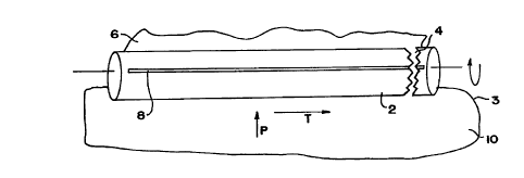
comprises a cylinder or roller 2 depicted in FIG. 1,
the roller being usable at a rotogravure printing
station. The roller 2 comprises a polished copper-
plated steel cylinder typically 0.1-3.0 meters in
circumference. The copper plate has a plurality of
liquid-carrying cells 4 engraved around the
circumference of the cylinder, as shown in exaggerated
form in FIG. 1. Those of skill in the art know that
the cells 4 may be engraved in the copper plate by
t~hn; ques such as diamond-stylus engraving, chemical
etching, laser inscribing, etc.
The roller 2 contacts a bath 3 of conductive liquid 10,
and is rotated so that the liquid 10 adheres to the
cells 4, is carried upward in the printing direction P,
and is deposited on a substrate 6 (to be described
below). A doctor blade 8 is mounted in the transverse
direction T and scrapes against the cylinder surface to
regulate the amount of ink carried on the roller 2 and
to remove excess ink therefrom.
CA 02224147 1997-12-08
WO 96/40r~ PCTAJS96/10011
_ g
FIG. 2 is a close-up view of prior art cells 4 engraved
in a roller for performing prior art rotogravure
picture printing. The plurality of cells 4 are
connected together in the printing direction P--that
is, circumferentially on roller 2. Each cell 4 is
substantially 160 by 250 microns, and has a central
portion 12 and a liquid c n; cation portion 14
disposed in the printing direction P. While the
central portion 12 of each cell 4 is deeper than the
liquid c- n i cation portion 14 thereof, liquid ink
nevertheless communicates readily in the printing
direction from cell to cell. The cells 4 may be
arranged with appropriate sizes, depths, and locations
on the roller 2 to produce a pleasing picture when the
ink is deposited on a substrate such as paper. While a
black and white picture may require only one such
roller, color pictures typically require four printing
stations, one for each of red, blue, yellow, and black,
the roller at each station bearing an appropriate array
of cells for that color.
In FIG. 2, cell walls 16 are disposed so as to separate
cells 4 in the transverse direction T. Ink must be
prevented from flowing in the transverse direction T
since this would produce a picture having unacceptable
horizontal or diagonal lines therein. Furthermore, the
cell walls 16 must support the doctor blade 8 which
regulates the ink and removes excess ink from the
roller.
FIG. 3 is a close-up view of the arrangement and
disposition of cells 4 according to the present
invention. According to the present invention, liquid
~. ;cation channels are also provided in the
transverse direction T between adjacent cells.
Preferably, each cell 4 also has a liquid communication
portion 18 exten~;ng in the transverse direction or in
CA 02224147 1997-12-08
W O ~/40r7~- PCT~US96/10011
-- 10 --
a direction oblique thereto. According to the present
. ho~; ment, the transverse liquid communication portion
18 intersects the printing direction liquid
communication portion 14 of an adjacent column of cells
4. In the printing process of this invention,
conductive liquid according to the present invention
(to be described below) is allowed to cross cell
boundaries in both the printing direction P and the
transverse direction T. Electrically conductive
pathways can thus be configured in any direction
parallel to or oblique to the printing and transverse
directions.
In FIG. 3, the cell walls 16 are oriented at plus and
minus 30-60 (preferably 45) degrees, respectively, with
respect to the axis of roller 2. As the roller 2
rotates in the printing direction P, the thus-disposed
cell walls 16 actually guide and regulate the flow of
conductive liquid according to the present invention in
the transverse direction to deposit an even and
continuous layer of conductive liquid in any direction
and in any configuration desired. The conductive
liquid 10 from the bath 3 is picked-up by the cells 4
as the roller 2 rotates in the bath. Excess liquid is
removed by the doctor blade 8, and the conductive
liquid according to the present invention is carried to
the substrate 6 where it is deposited directly thereon.
While the central portion 12 of each cell 4 may be
deeper than the liquid communication portions 14 and 18
thereof, when the liquid is deposited on the substrate
6, the free-flowing liquid according to the present
invention tends to equalize readily in all areas where
the solution contacts the substrate 6. Thus, uniform
and continuous electrical pathways are formed on the
substrate. The disposition of cell walls 16 depicted
in FIG. 3 also provides support for doctor blade 8 in
CA 02224147 1997-12-08
W O 96/40522 PCTAJS96/10011
-- 11 --
the transverse direction T around the entire
circumference of roller 2.
FIG. 4 is a cross-section taken along line 4-4 of FIG.
3, and depicts the relationship between cell central
portion 12, li~uid communication portions 14 and 18,
cell walls 16, and the doctor blade 8. Sufficient
voids are provided in roller 2 below the doctor blade 8
to carry the conductive liquid 10 from the bath 3 to
the substrate ~. The depth of central cell portion 12.
is substantially 10-100 (preferably 40 microns), and
the depth of liquid communication portions 14, 18 is
substantially 20-60 (preferably 20) microns. Since the
columns of cells 4 in the present invention are
disposed much closer together in the transverse
direction, approximately 200 columns of cells are
provided per inch in the present embodiment, as
compared to 165 columns of cells per inch in the prior
art roller depicted in FIG. 2.
While the press according to the GRAVCO-PROCESSTM has
~een described above with respect to a roller similar
~ to one used in rotogravure printing, it is to be
understood that the press according to the present
invention may comprise a flat plate, may be made of a
photopolymer or plastic, and may utilize technology
similar to rotogravures flexographic, offset gravure,
offset, and letter press printing. All such similar
and equivalent presses are, of course, included within
the scope of the appended claims.
~ 3. The Conductive Li~uid
According to the present invention, the conductive
liquid (including conductive paste) utilized to form
the electrically-conductive pathways may comprise a
solution, a suspension, or a paste having a viscosity
substantially within a range of lo to 50,000 cp; more
CA 02224l47 l997-l2-08
W O 96/40522 PCT~US96/10011
- 12 -
preferably within the range of 10 - 200 cp; even more
preferably within the range of 10 - 50 cp. The liquid
preferably comprises a solvent and/or water (or a
combination of solvent and water), solids (resins and
conductive powder), and plasticizers. Solventless
liquids may also be used and oligimers will replace the
~olvent and/or water.
Preferably, the solvent comprises between substantially
55 percent and substantially 85 percent by weight of
the liquid. (If water is used, it will comprise 25-65
percent by weight of the liquid). Even more
preferably, the solvent is between substantially 65
percent and substantially 80 percent by weight; and
even more preferably between 70 and 75 (most preferably
72) percent by weight of the liquid. The solvent
preferably includes esters, ether glycol, and ketones.
Between substantially 60 percent and substantially 95
percent by weight of the solvent are esters or
equivalents. The most preferred embodiment includes 80
percent by weight of esters in the solvent. The
solvent also should include between substantially 3
percent and substantially 20 percent, by weight ether
glycols, and most preferably 10 percent. Finally, the
solvent includes between substantially 3 percent and
substantially 20 percent by weight of ketones, most
preferably 10 percent. Of course, water-based
dispersions could be used in lieu of the solvent- based
solution. In this instance, wetting agents and foam
suppressors, known to those of skill in the art, may
also be used.
The preferred conductive liquid also includes between
substantially 10 percent and substantially 40 percent
by weight of solids, most preferably 25 percent. The
solids preferably include substantially 5 percent to
substantially 90 percent (preferably 20 percent to 90
CA 02224l47 l997-l2-08
W O 96/40522 PCTAUS96/10011
- 13 -
-
percent) by weight of polymer resin (polyester) -- a
polar resin. Preferably, the polymer resins comprise
72 percent by weight of the solids.
The solids preferably include between substantially 3
percent and substantially 80 percent (preferably 10
percent to 80 percent) by weight of a conductive
powder, most preferably 28 percent. The conductive
powder comprises particles in the range of
substantially 3 to substan~ially 50 (preferably 5 - 10)
microns in diameter and may comprise aluminum,
graphite, gold, silver, carbon, or other known
conductive materials, or any combination thereof. The
choice of conductive powder will vary in accordance
with the component being designed, the width and
thickness of the printed electrical pathway, and the
current required to be carried therethrough.
Additionally, the conductive liquid according to the
present invention preferably includes between
substantially 1 percent and substantially 7 percent by
weight, and most preferably between 2 and 3 percent by
weight, of plasticizers. A preferred plasticizer is
Dioctylphatalate.
Equivalents of the above-described electrically-
conductive liquid may include water in addition to or
as a replacement for the solvent. When replacing the
solvent, the water comprises 25-65 percent by weight of
the liquid. Solventless liquids can also be provided
where oligimers replace the solvent and comprise
substantially 25-60 percent by weight of a liquid. In
this formulation, the conductive powders comprise 15-50
percent by weight of the liquid, and the plasticizers
preferably comprise 1-5 percent by weight of the
liquid. The oligimers may be activated by heat, light,
electromagnetic radiation, etc.
CA 02224l47 l997-l2-08
WO 96/40522 PCTAJS96/lO011
- 14 -
The conductive liquids described above are merely
illustrative and are designed to be used in signal
lines for carrying low-power signals in the printed
electrical circuit. Of course, a wide variety of
solutions, suspensions, and/or pastes may be adapted
depending upon the use for which the circuit component
is designed. For example, signal lines and power lines
will be highly-conductive. On the other hand, liquids
used to print resistors will have a much lower
conductivity. Magnetic liquids may be used to prepare
inductive circuits, and electroluminescent liquids may
be used to produce light-emitting circuitry. Of
course, all such equivalent conductive liquids are
enc~mr~ed by the present invention.
Furthermore, pigments may also be included in the
conductive liquid to provide ornamental as well as
functional features. Thus, not only may the conductive
liquid perform an electrical circuit function, it may
also be used as a label to provide information
regarding the source of the goods or the product
contained within the package. For example, an
electrical circuit used in a child's toy may be
arranged so that the circuitry spells out the toy name
and/or toy instructions.
In a preferred embodiment, a conductive liquid for use
in directly printing signal lines may be manufactured
by pouring into a contA;ner substantially 88 percent by
weight of the final liquid of AQUADAGTM liquid produced
by Acheson Colloids Co., 1600 N. Washington, Port
Huron, Michigan. In a separate container, 1/2-2
percent by weight of plasticizer (preferably
Dioctylphatalate) is premixed by hand at ambient
temperature with 10 percent by weight of solvent,
esters, and/or ether glycol. After pr- ;~ing the
CA 02224147 1997-12-08
WO ~6/40'??~ PCTAJS96/10011
-- 15 --
plasticizer and solvent, the premix is added to the
AQUADAGTM and mixed by air mixer for 15-20 minutes.
.
4. The Process
The GRAVCO-PROCESSTM for directly printing an electrical
circuit component onto a substrate is schematically
depicted in FIG. 5. The process will be described with
reference to the manufacture of a computerized pill
dispenser article which is depicted in FIG. 6. Such an
article is used to monitor and schedule the
dispensation of drugs in pill form. In FIG. 6, a pill
in a plastic blister is disposed over top of each
curved conductor line. The substrate beneath the
conductor line is aluminum foil or some other easily-
tearable surface. The pill dispenser is placed in a
computerized monitoring device (not shown), and the
device will send signals through the signal lines to
determine the electrical continuity of each line. As
each pill is dispensed, it is pushed downward through
the aluminum substrate, severing the signal line to
indicate that that pill has been dispensed. A display
on the device will indicate which pills have been
dispensed and when; the display may also indicate when
the next pill should be dispensed. Where the pill
dispenser has on-board signal generating, memory, and
display circuitry, it is even possible for the
dispenser itself to determine the time at which the
pill was ~; sp~nC~, and the time the next pill is
scheduled to be dispensed.
The process of FIG. 5 feeds a substrate (web) of 1 mil
aluminum foil 52 from a roller 54 to printing station 1
which is configured similar to a well-known rotogravure
printing station. At printing station 1, a roller 56
sits in a bath of dielectric coating 58 and rotates to
deposit a thin but continuous layer of dielectric over
the bottom surface of aluminum sheet 52. The
CA 02224l47 l997-l2-08
W 0~6/40~22 PCT~US96/10011
- 16 -
dielectric coating is preferably a polymer resin and
solvent solution 10 microns thick which prevents any
electrical contact with the aluminum sheet 52. A pinch
roller 60 is disposed on the other side of aluminum
foil 52 and ensures a uniform dispersal of dielectric
coating on the aluminum sheet 52.
Printing station 1 also includes a dryer 62 which dries
the dielectric coating on the sheet 52. The dryer may
comprise a hot air oven (5 feet long @ 200~ C.)
directing an air blast at the foil for 0.5 - 1.5
seconds.
After exiting printing station 1, the sheet 52 is fed
to printing station 2 where a roller 64 (for example,
the roller 2 described above) sits in a bath 66 of
conductive liquid #1 at ambient temperature. Since the
conductive liquid may contain powders, an ink agitation
system may be used in bath 66. This first conductive
liquid will be used for signal lines, power lines, and
other high-conductivity uses, and may comprise the
conductive liquid described above. The roller 64 will
have a pattern of cells 4 disposed in the printing
direction P, in the transverse direction T, and in any
directions oblique thereto. Preferably, the roller 64
is wide enough to simultaneously print seven electrical
circuits as depicted in FIG. 6. Again, a pinch roller
68 will ensure a proper printing, and a dryer 70 will
dry the conductive liquid #1. While the dryer 70 may
comprise a hot air oven, as described above, preferably
it is a microwave or radio frequency generator (e.g.,
27 megahertz) which will dry the conductive liquid
internally and not just the skin, which is a problem
with air dryers. Thus, at printing station 2 the
electrical circuit and its components are directly
printed in a single operation without the post-printing
operations described earlier.
CA 02224l47 l997-l2-08
W O 9('4~ PCT~US96/10011
- 17 -
At printing station 3, a print roller 72 will apply
conductive liquid #2 from bath 74 onto the sheet 52.
Conductive liquid #2 is less conductive than liquid #1
and is used to deposit components such as resistors.
Again, a pinch roller 76 and a dryer 78 are used to
print and dry the conductive liquid #2. Alternatively,
printing station 3 could apply an additional layer of
conductive liquid ~1 over the previous layer to form a
thick circuit, such as a power line.
Where the circuits require an insulating layer to be
deposited on top of conductive liquids #1 and #2, a
printing station 4 may be provided. At printing
station 4, the print roller 80 sits in a bath of
insulator coating 82 (such as a lacquer) to deposit a
specified thickness of insulation over top of the
conductive liquids. The insulator coating is deposited
at any thickness required by the circuit. For example,
to form a capacitor, the insulator layer may be 1
micron to 1000 (preferably 500) microns thick.
However, if a push-pad switch is being produced, the
thickness of the insulator layer may be less, such as
10 microns. As with the previous printing stations,
printing station 4 includes a pinch roller 84 and a
dryer 86.
Alternative to printing station 4, or in addition
thereto, a laminating insulator material 88 may be
applied from a roller 90. For example, the insulator
88 may comprise paper, polymeric plastic, or any other
flexible insulating substrate or web. The insulator 88
- may have holes or electrically conductive patterns
therein to allow electrical contact between the
conductive liquid #1 and later-deposited conductive
layers, if desired. The holes in insulator 88 may be
small enough so that contact is only established by
pushing the two conductive layers together through the
CA 02224147 1997-12-08
WO 96/40522 PCT~US96/10011
- 18 -
insulator 88 to produce, for example, a push-pad
switch. In addition to laminating an insulator
material, a roller may be provided for laminating one
or more conductive layers (such as metallic foil) for
additional signal or power channels, or for radio
frequency shielding, as desired. Specific circuit
details will be described later.
In FIG. 5, the sheet 52 is then transported to printing
station 5 where a print roller 90 applies conductive
liquid #3 from a bath 94 to the sheet 52 on top of the
insulating layer. Conductive liquid #3 may comprise a
highly-conductive liquid similar to conductive liquid
#1. Again, this liquid may be used for upper-layer
signal lines, power lines, capacitors, etc. A pinch
roller 96 and a dryer 98 are also provided at printing
station 5. Again, one or more layers of conductive
liquid #3 may be printed, as desired.
If desired, a printing station 6 may be provided
wherein any one or more of specialty liquids and/or
printing inks may be applied. For example, special
effects liquids may be provided such as thermochromic
liquids, electrophosphorescent liquids, magnetochromic
liquids, electrochromic liquids, zinc oxide (glow-in-
the-dark) liquids, electroluminescent liquids, magnetic
liquids, etc. If desired, more than one printing
station may be provided for applying a series of such
specialty liquids. In addition to, or as an
alternative to the specialty liquids, graphic printing
inks may be provided for affixing well-known labels,
instructions, or decorations to the product. These
inks may include conductive liquid so that the graphic
image may comprise an electrical circuit and/or
component. At the printing station 6, a print roller
100 transfers the specialty liquid and/or the printing
CA 02224147 1997-12-08
WO 9C/~ PCT~US96/10011
-- 19 --
ink from a bath 102 and applies it to sheet 52 aided by
a pinch roller 104 and a dryer 106.
At station 7, a spiked roller 108 is used to provide
appropriate layer interconnects between the upper and
one or more lower layers of conductive liquid. Each
spike 109 will penetrate through the conductive liquid
#3, the insulating layer, and the conductive liquid #1
and/or #2 to make an electrical contact between the
upper and lower conductive layers. If dryers 98 and
106 are not activated (or are preferably modulated),
the conductive liquid #3 will still be in liquid or
semi-liquid form when spike 109 penetrates through the
insulating layer to the lower conductive layer. The
conductive liquid will move through the interconnect
hole and make a good electrical contact with the lower
conductive layer. Preferably, the spiked roller will
be disposed before the upper conductive layer printing
station so that the printing of the upper layer will
force liquid under pressure into the interconnect hole.
Of course, the number, location, and depth of each of
these spikes 109 may be specially designed depending
upon the particular circuit which is being
manufa~LuLed. As an alternative, the roller 108 may
sit in a bath (not shown) of conductive liquid to
further enhance the inter-layer electrical contact. At
station 7, the spiked roller may be a punch roller
press, a male-female die; or a backing roller or other
device 110 may be used to provide proper support for
the penetrating spikes 109. A dryer 112 may be used,
if desired, to dry the conductive liquid connecting the
conductive layers. Alternatively, crimps, rivets or
other electrical conductors (preferably those which can
be installed in an in-line process) may be used to
electrically couple two or more conductive layers.
CA 02224147 1997-12-08
WO 96/40522 PCTAUS96/10011
- 20 -
Station 8 is equipped to provide a protective coating
over the top of the finished electrical circuit. The
roller 114 applies a protective coating from bath 116
to cover the surface of the finished product. The
S protective coating may comprise lacquer, polymeric
plastic, etc. A pinch roller 118 (or smoothing bar)
and a dryer 120 may be provided, if desired. A
cutting/separating unit 122 may be provided to cut,
separate, and stack separate electrical circuits.
Alternatively, the sheet containing the printed circuit
boards may be rewound onto another roller for shipping
and subsequent processing. These units are reasonably
well known to those of skill in the art and will not be
described in further detail herein.
The process described above with respect to FIG. 5 is
capable of infinite variation depending upon the
electrical circuit being produced. For example, three,
four, or five conductive layers may be provided with
(or without) interspersed insulating layers.
Conductive liquids may be printed on top of each other
to build thick components, e.g., 5 layers for a power
line. The spiked roller 108 may be provided at any
station or in between stations depending upon the
interconnections required among the various conductive
layers (e.g., to interconnect layers 1 and 2, and then
4 and 5). The insulating layers may be transparent or
may be light-blocking. The type of conductive liquid
and the pattern dimensions may be adjusted to achieve
desired electrical characteristics such as resistance
ohms, capacitor picofarads, the wattage of any power
line, current, inductance, reactance, etc. The
characteristics of the insulator coatings may be chosen
for desirable insulating properties such as
breakthrough voltage, tangent losses, etc. Additional
aluminum sheets and/or conductive layers may be
inserted via roller, as with the insulator roller 90,
CA 02224147 1997-12-08
WO 96/40522 PCTrUS96/10011
- 21 -
at any point in the process. The aluminum sheet may
act as a ground plane for all of the electrical
components, or may carry power to all of the circuits
disposed above the dielectric layer, or may shield the
circuit from electromagnetic or static electric
interference.
As another alternative, an additional station (not
shown in FIG. 5) may be provided at any point in the
process for checking the quality of the already-printed
circuits. For example, a roller may be provided having
a plurality of electrodes disposed thereon which are
arranged (registered) to come into contact with
appropriate terminals on the sheet 52 passing beneath
the roller. The electrodes on the roller will be
activated (pulsed) to run continuity checks, resistance
~h~ck~, voltage checks, amperage checks, etc., through
the terminals in contact with the roller electrodes,
etc. High-speed in-line quality checks will ensure a
highly reliable product by quickly identifying failed
circuits for removal at cutting/separating device 122.
Alternatively, defective products may be marked as the
sheet 52 is being rewound.-
As yet another alternative, the process depicted in
FIG. 5 may be "looped" from station 8 back to station 1
80 that further additional conductive and insulating
layers may be deposited and interconnected, as
required.
As a further alternative, the electrical circuit may be
formed on a flexible substrate (such as a 1 to 15
(preferably 1) mil thick polymeric plastic), and then
bonded to a rigid substrate, such as an epoxy-
fiberglass composite. Such a product is still far less
~pe~cive to produce than the known methods of
producing known rigid printed circuit boards.
CA 02224147 1997-12-08
WO 96/405Z2 PCTAJS96/10011
- 22 -
While the substrate depicted in FIG. 5 comprises a
flexible aluminum foil, other flexible substrates may
be utilized, such as polymeric materials to include
films, plastics, combinations, coextrusions,
laminations, non-woven polymeric fabrics, cloth, paper,
wool, etc. Also, while flexible substrates are
preferred, semi-rigid or relatively rigid substrates
can also be used including polyamide, polycarbonate,
polyester, mylar, lexan, kevlar, cardboard, acrylics,
acetate, foamed or foamable polymers, fiberboard, etc.
Rigid substrates can be provided in many forms
including for example, ceramics, glass, plastics, paper
compositions, or composite substrates such as epoxy-
fiberglass, epoxy-paper laminate, etc.
The conductive liquid printed according to the GRAVC0-
PROCESSTM may be of any practical thickness, length, and
width desired. The thickness may vary from one
molecular layer to 200 microns, or even up to 500
microns if desired. Since the liquid can be made to be
relatively free-flowing, very thin, closely-spaced
components may be printed. This flexibility provides
the circuit designer with a wide range of circuit
component values which can be accommodated by the
GRAVCO--PROCESSTM.
5. The Articles
An extraordinarily wide variety of useful articles may
be produced according to the GRAVC0-PROCESSTM, and hence
many products that have never been practical or cost-
effective will become available as a result of this
invention. For example, FIG. 6 depicts one article
useful for the reliable dispensation of drugs. Some
patients are forgetful or uncertain as to whether and
when certain drugs have been or should be dispensed. A
drug dispensation system in which it is positively
CA 02224147 1997-12-08
W O ~C/~ ? PCT~US96/10011
- 23 -
known when the last drug was dispensed and when the
next drug should be dispensed is quite important. FIG.
6 depicts a plan view of a drug dispenser article which
may accurately and reliably schedule drug treatment.
The circuit shown in FIG. 6 may be produced according
to the GRAVC0-PROCESS~M described above, and its use
will be described below. Drug dispenser article 200
has a plurality of electrodes 202 disposed along one
edge thereof. The electrodes 202 are configured to be
inserted into a computerized drug scheduler (not
shown). Signal lines 204 extend from electrodes 202
and back to matching electrodes 206, making a
continuous electrically conductive path from electrodes
202 to electrodes 206. The signal lines 204 include
curvelinear portions 208 which are preferably disposed
on aluminum foil immediately beneath a pill 210
contained within a plastic blister 212.
In order to dispense a pill, the patient pushes the
pill 210 through the aluminum foil at the bottom of the
article 200, thus severing signal line 208. The
severing of the signal line 208 is detected by the
computerized scheduler, and the time is noted therein.
The computer now has a schedule indicating the identity
of and time that each pill was removed from the article
200. The patient merely observes the display of the
computerized scheduler to determine when the last drug
was taken, and when the next drug is scheduled to be
taken.
FIG. 7 is a cross-section view of a portion of the
article 200 as viewed along lines 7-7, of FIG. 6. The
flexible aluminum foil 52 has disposed thereon a
dielectric coating 58, as has been described above with
reference to FIG. 5. Signal lines LS1 and Ls2 are
deposited thereover and carry signals. A thicker line
Lp may be provided as a bus line for communication, as
CA 02224l47 l997-l2-08
W09C/4~ PCT~US96/l0011
- 24 -
a circuit-matching resistor, or as a power line for
carrying power, if required. Disposed over top of the
signal lines is a protective coating 116 of, for
example lacquer, as described earlier with respect to
FIG. 5.
FIG. 8 is a cross-sectional view of a number of
alternative circuit components which may be produced
according to the GRAVCO-PROCESSTM described above. All
circuits are depicted as being printed on a substrate
layer 53, such as 1-2 mil polymeric plastic. A
capacitor Cl is provided having plates 802 and 804
separated by an insulating layer 806. The capacitor
plates 802, 804 and the insulating layer 806 are
dimensioned to produce the appropriate capacitance
required for the circuit. Of course, the capacitor
plates 802, 804 are coupled to other conductive
circuitry (not shown).
A switch SWl is also shown in FIG. 8 and may comprise
electrodes 808 and 810. The electrodes are separated
by an insulating layer 812 which may comprise an
insulating material having a plurality of voids or
holes therein. pll~hing down on electrode 810 will
cause it to make contact with electrode 808, thus
closing switch SWl. If the insulating layer 812 has
elastic properties, releasing pressure on electrode 810
will cause the switch to open.
Energy source (battery) El is also shown in FIG. 8 and
comprises electrode 816, electrolyte 818, and electrode
820. The electrolyte 818 preferably comprises micro-
encapsulated liquid electrolyte (e.g., alkalines) which
may also be deposited via the GRAVCO-PROCESSTM printing
techniques described above. Alternatively, the
electrolyte may comprise a liquid or a gel encased in a
plastic blister which is deposited on the electrode 816
CA 02224147 1997-12-08
W O 96/405Z2 PCT~US96/lOOll
- 25 -
in an in-line process, as depicted in FIG. 5 for
insulator 88. When the power source is ready for
activation, the electrolyte 818 may be activated by the
user pressing thereon, or some other process can be
applied for causing the electrolyte 818 to make contact
with both electrodes 816 and 820 (e.g., ~?chAn;caI
pressure, electrical activation, heating, photo-
stimulation, etc.). Such a power source may be a
simple short-term, one-shot power supply, or it may
provide longer-lasting, higher-power similar to known
1.5-volt batteries, depending upon the number of
electrodes and the type of electrolyte used. In a
preferred embodiment, a battery may be printed by
printing a carbon electrode on a substrate, depositing
a dry alkaline on top of the carbon electrode, and
printing a zinc electrode over the dry alkaline. The
zinc will have a plurality of holes therein so that
dipping the battery in water will liquidify the
alkaline thus activating the electrolyte to power the
battery. If higher voltages are needed, a plurality of
such batteries may be connected in series, or an
increase in battery current may be achieved by
connecting a plurality of such batteries in parallel.
Also depicted in FIG. 8 is a simple resistor R1 which
may provide a r~sistance depending upon the thickness,
width, length, and type of conductive liquid used
therefor.
FIG. 9 depicts further articles which may be produced
according to the GRAVC0-PROCESSTM described above. FIG.
9 shows how a through (or interconnect) hole 822 which
may be provided between signal lines LS1 and LS2 The
through hole 822 may be produced, for example, by the
spiked roller 108 depicted in FIG. 5. FIG. 9 also
depicts a light electrode LE1 which may, for example,
comprise an electroluminescent layer. Upon application
CA 02224147 1997-12-08
W O 9tl4c-~2 PCTAJS96/10011
- 26 -
of the appropriate current, LE1 will emit photons for a
time and intensity ~ep~n~;ng upon the composition of
the solution and the applied current and voltage.
.
FIG. 10 depicts a theft-detection tag produced
according to the GRAVCO-PROCESSTM described above. Such
tags may also be used for registering inventory,
identifying products, tracking hospital patients
(newborns), anti-shoplifting, product labeling, etc.
The anti-theft tag of FIG. 10 comprises a resonant
circuit printed on both the top and bottom of an
insulating substrate, for example, paper, cardboard,
polymer films, nonwoven fabrics, cotton cloth, silk,
etc. The top and bottom circuits may be connected by
folding, welding, or interconnecting as described above
with reference to FIG. 5. The resonant circuit
comprises a conductive coil 900 having a thin, 1 mm
long, 0.25 mm wide bridge-portion 902 disposed therein.
When the theft-detection tag passes through a detector
unit (not shown~, RF energy emitted by the detector
unit causes the circuit to resonate and act as a
transmitter, giving off RF energy which may be detected
by the detector. If the product has been properly
purchased, a microwave capacitor 904 disposed near the
cash register may emit a low-power microwave ray to
burn and sever the bridge 902, thus decoupling the
resonant circuit and permitting the tag to be removed
from the store through the detector apparatus without
alarm. Of course, other ways of decoupling the
resonant circuit may be used, such as mechanical
severing, magnetic alteration, etc. Very few articles
of clothing currently have theft-detection circuits
affixed thereto because known circuits are not cost-
effective. However, according to the GRAVCO-PROCESSTM,
cotton or silk clothing labels bearing both product
information and anti-theft circuitry may be produced in
an in-line, high-speed process at low cost.
CA 02224147 1997-12-08
W O 96.'4Qr~?- PCTrUS96/10011
- 27 -
A wide variety of other articles may be produced
according to the GRAVCO-PROCESST~ described above. For
example, heating circuits can be printed on plastic
sheeting which is laminated to a thermoformable plastic
substrate, the laminate being subsequently thermoformed
into a three ~; e~ional product. such a process can
produce food trays made of foamed polymers may have
heating circuits printed in the bottom thereof, so that
food may be heated with an available electrical
circuit, for example, a cigarette lighter in a car.
Such a heating element may also be printed in coffee
cups, soup cups, hot cereal containers, baby bottles,
etc. The circuit need only have two electrodes and an
appropriate number of resistors disposed near the
product to be heated. Also, food products can be
heated within flexible pouches with printed heating
elements.
Other heating applications are also susceptible to the
GRAVCO-PROCESSTM described above. For example, space
heaters (e.g., for use in a van or trailer) may be
produced by thermoforming large sheets of a semi-rigid
substrate (e.g., foamable polymeric composites).
Printed on the substrate (prior to thermoforming) would
be a plurality of heating elements produced according
to the GRAVCO-PROCESSTM. The heating elements could be
readily configured to provide high heat or low heat and
for a particular space desired. The heating elements
could even be produced in interconnectable modular
form. Power could be provided through a vehicle
- cigarette lighter, from a vehicle alternator, or from a
wall outlet for use in a building space heater.
Heating elements may also be printed on cloth or on the
non-woven polymer fabrics discussed above. This could
result in inexpensive heated products such as heated
CA 02224147 1997-12-08
WO 96/4C'?~ PCT~US96/10011
- 28 -
blankets, heated towels, heated socks, heated mittens,
heated caps, heated clothes, heated automobile seats,
heated furniture, etc.
Furthermore, large sheets of polyethylene having heated
elements printed thereon may be produced for use in hot
houses for personal or ~- ~~cial use. The heating
elements may be designed to produce a wide range of
btu's depending on the type of hot house being
assembled.
.Alternatively, electrical circuits produced according
to the GRAVCO-PROCESSTM may be used to cool products.
It is well known that semi-conductor materials (P-N
junctions) may generate heat or absorb heat dep~n~; ng
upon the current (and direction of current) applied
thereto. All of the above-noted heating applications
may have complementary cooling applications which can
be satisfied according to the electrical circuits
produced by the GRAVCO-PROCESSTM. As one example, the
foam labels adhered to soda bottles may have circuitry
printed therein to absorb heat from the bottle, thus
cooling the liquid. The cooling circuitry may be
coupled to an external power source, or a power source
may be printed into the label, as described above.
Thus, the GRAVCO-PROCESSTM may produce a great number of
products capable of being heated and/or cooled.
Electrically conductive liquids may also be printed
according to the GRAVCO-PROCESSTM on documents requiring
authentication, such as bonds, stocks, currency, etc.
Electrical circuitry having particular characteristics
may be printed on the document and later verified with
a small electrical authenticator which ascertains the
characteristics of the electrical circuit printed on
the document.
CA 02224147 1997-12-08
W O ~'40-~ PCTAJS96/lO011
- 29 -
Furthermore, electrically conductive liquids may be
printed according to the GRAVCO-PROCESSTM to perform the
r function of product registration in well-known in-line
bag-making, sheeting, or pouch-making processes and in
any process requiring position detecting and
triggering. Currently, a large black or dark
registration mark is provided on a bag web. An optical
reader dete ;ne~ the location of the registration mark
to control the feeding, and cutting of the printed web.
However, optical readers are susceptible to dirt and
other reliability problems. By using a conductive ink
as a small registration mark, a small roller (or wheel)
with one or more electrodes thereon may be used to
detect the passage of the conductive ink registration
mark, e.g., with a continuity check.
Microwave susceptors may also be printed into products
to be used in microwave ovens, such as microwave
popcorn bags or boxes (plastic or paper). Currently,
microwave susceptors must be mechAn;cally (or manually)
inserted into pouches or between layers of a microwave
container, (e.g., a popcorn bag). With the GRAVC0-
PROCESSTM, such susceptors may be printed on or within
container layers in an in-line, low-cost process.
Indeed, the
GRAVC0-PROCESSTM may combine printing electrically
conductive circuits with ornamental labels, as
di~cll~ce~ earlier. Thus, the name of the microwave
popcorn manufacturer may be printed with an
electrically-conductive liquid so that the
manufacturer's name itself acts as a microwave
susceptor.
Electroluminescent liquids may be advantageously used
in light-up displays attractive to the consumer. For
example, soda cans may be printed with
electroluminescent liquids, power lines, and terminals
CA 02224147 1997-12-08
WO 96/40S22 PCTrUS96/10011
- 30 -
using the GRAVC0-PROCESSTM described above. The soda
can display at the store may have matching electrodes
and a power source such that the displayed soda cans
actually light up with the manufacturer's name and/or
trademark.
Furthermore, tamper-evident packaging may also be
created utilizing electrical circuits produced by the
GRAVC0-PROCESSTM described above. For example, signal
lines may be printed on shrink-wrap product coverings
such that the signal lines break to show tampering. A
simple circuit located at the cash register would be
used to detect broken signal lines indicating that the
package had been tampered with.
As described above, any known or useful electrical
circuit can be produced according to the GRAVC0-
PROCESSTM including, but not limited to, signal lines,
power lines, connectors, switches, antennas, induction
heaters, radiant heaters, coolers, radiation
reflectors, diodes, capacitors, transistors, resistors,
inductors, coils, batteries, sensors, fuel cells,
piezoelectric elements, light emitting circuits,
photovoltaic cells, photo-imaging cells, etc.
6. Conclusion
Thus, what has been described above is a method and
apparatus for the high-speed mass production of
electrical circuit components by directly printing
electrically conductive liquids onto a substrate
without post-printing processes. The GRAVC0-PROCESSTM
is far superior to the best-known printed circuit board
te~hn;ques, such as silk-screen. The GRAVC0-PROCESSTM
can produce printed circuit boards 10-50 times faster
than silk-screen processes. The precision and
geometric tolerances produced according to the present
invention are also far superior to silk-screening since
CA 02224147 1997-12-08
W O ~6/40!~ PCTAJS96/10011
- 31 -
a stencil does not have to be pulled away from the
substrate allowing the thick ink to cause dispersion at
the edges. The silk-screen process can produce signal
line the order of 500 microns, whereas the present
invention can produce signal lines tolerances an order
of magnitude narrower. Silk-screen inks are also quite
expensive, from 600-700 dollars per pound, orders of
magnitude more expensive than the present invention.
In addition, a large amount of ink wastage is seen in
silk-screen processes, where the present invention will
waste very little ink. The present invention can
miniaturize or downsize circuits because the direct
printing process can produce much finer and smaller
dimensions than silk-screen stencils. For example,
silk-screen processes can only approximately space
signal lines 2 millimeters apart, whereas the present
invention can space signal lines approximately 0.1
millimeters apart. Further, the GRAVCO-PROCESST~ can
easily produce multi-layer circuitry, whereas silk
screening can only produce a single layer. Finally,
silk-screen processes cannot print circuit boards on
flexible substrates, whereas the present invention can
print on one mil flexible substrates such as plastic,
paper, or aluminum foil. Accordingly, the present
invention can produce electrical circuit components
and/or electrically circuits at-a fraction of the cost
and in a fraction of the time of the best-known current
printed circuit board t~chn; ques.
While the present invention has been described with
what are presently considered to be the preferred
- embodiments, the claims are not to be limited to the
disclosed embodiments. To the contrary, the claims are
intended to cover various modifications and equivalent
structures and functions as are apparent from the
appended claims.