Note: Descriptions are shown in the official language in which they were submitted.
CA 02224189 1997-12-09
WO 97/39308 PCT/US97/05982
1
WAVELET ANALYSIS FOR LASER ULTRASONIC
MEASUREMENT OF MATERIAL PROPERTIES
FIELD OF THE INVENTION'
This invention relates generally to non-destructive
materials characterization systems and methods and, in
particular, relates to methods and apparatus for
determining at least one property of a material using a
laser ultrasonic approach.
BACKGROUND OF THE INVENTION'
Many types of materials processing require real-time
monitoring of physical characteristics such as, by example,
temperature, material phase, case hardening depth, and
thickness. Often the processing environment or motion of
the material makes direct contact measurement impossible.
Conventional remote techniques have typically relied on the
radiative properties of the material, as i~ the case with
optical pyrometry for temperature measurement. However,
emissivity changes during processing, and reduced
sensitivity at low temperatures, preclude the use of this
technique in many application.
~ A more suitable method for remote sensing of material
properties is laser ultrasvnics, in which a short intense
laser pulse (impulse beam) generates a sudden localized
thermal expansion which subsequently launches ultrasonic
waves through the material. The passage of the waves is
detected a short distance away on the surface of the
material by a probe beam from an interferometer, and the
CA 02224189 1997-12-09
WO 97!39308 PCT/US97/05982
2
speed of the ultrasound waves is calculated from the time
of flight. The velocity of the wave propagation depends on
the elastic constants of the target material, and thus is
a function of the material properties, such as temperature.
The separation of the two optical beam paths (impulse and
probe) can be relatively small, enabling only localized
material properties to be evaluated and mapped. This
technique has been used extensively for nondestructive
evaluation (NDE) and materials characterization. Reference
in this regard can be made to Hutchins, D. and Tam, A.C.,
"Pulsed Photoacoustic Materials Characterization", IEEE
Transactions on Ultrasonics, Ferroelectrics, and Frequency
Control, Vol. UFFC-33, No. 5, September 1986, pp. 429-449.
However, in some cases the broadband laser ultrasound
generation results in a surface displacement that is a
complex function of frequency dependent wave velocities,
making accurate time-of-flight measurements difficult.
This problem can be further compounded by the typically low
signal to noise ratios.
A standard signal processing technique is Fourier analysis,
which presumes that a given signal can be expressed as the
superposition of a series of sine waves. Each sine wave
component has a given frequency and amplitude, where the
amplitude corresponds to the energy of the original signal
which is contained within that frequency. Thus a plot of
amplitude versus frequency can readily show the dominant
frequencies. This signal processing is useful for
identifying predominant frequencies in periodic signals
over many cycles, but since it has poor time-frequency
localization it does not readily accommodate the case of a
short, transient signal as is found in most laser
ultrasonics applications.
A representative, but not exhaustive, list of U.S. Patents
. . CA 02224189 1997-12-09
WO 97/39308 PCT/US97/05982
3
in the laser ultrasonics and related technical areas
include the following: U.S. Patent 3,601,490, issued
8/24/71 to K. Erickson and entitled "Laser Interferometer":
U.S. Patent 3,694,088, issued 9/26/72 to J. Gallagher et
al. and entitled "Wavefront Measurement"; and U.S. Patent
4,633,715, issued 1/6/87 to J. Monchalin and entitled
"Laser Heterodyne Interferometric. Method and System for
Measuring Ultrasonic Displacements".
Also of interest is U.S. Patent 5,286,313, issued 2/15/94
to Thomas J. Schultz, Petros A. Kotidis (an inventor of the
subject matter of this patent application), Jaime A.
Woodroffe, and Peter S. Rostler. The preferred embodiment
of the system described in this patent employs an XeCl
impulse laser in combination with a Helium-Neon based
polarizing interferometer to provide, by example, remote
detection of a temperature of a workpiece.
OBJECTS OF THE INVENTION:
It is a first object of this invention to provide an
improved laser ultrasonics materials measurement system.
It is a second object of this invention to~provide a laser
ultrasonics system that employs wavelet analysis to
accurately determine a material property of interest, such
as temperature, thickness, surface properties, and coating
thickness.
It is a further object of this invention to provide a laser
ultrasonics system that employs wavelet analysis to
accurately determine a temperature of a silicon wafer
during thermal processing of the wafer.
CA 02224189 1997-12-09
WO 97/39308 PCT/US97/05982
4
SUMMARY OF THE INVENTION
The foregoing and other problems are overcome and the
objects of the invention are realized by methods and
apparatus in accordance with embodiments of this invention,
wherein a laser ultrasonics technique is used to
characterize a composite dispersive response signal from a
sample under analysis, such as a semiconductor wafer.
Rather than measuring individual acoustic wave velocities
at specific frequencies, an entire dispersive response
signal is analyzed. In a presently preferred~embodiment of
this invention the entire dispersive response signal is
analyzed using a wavelet-based technique, such as a
discrete wavelet transform analysis technique. The discrete
wavelet transform analysis technique is shown to provide an
accurate, non-contact measurement of the temperature of the
wafer.
It is shown that the discrete wavelet transform captures
information expressive of the overall pattern of a signal,
and therefore quantifies more than just the time of flight
of the ultrasound signal. For example, if there is a change
in the relative amplitudes of the ultrasound signal at two
different frequencies, indicating a shift in the input
energy distribution to the two frequencies, the times of
flight may remain the same. Wavelet analysis, however, is
shown to indicate the redistribution of the energy, which
is indicative of a change in material properties, such as
temperature.
BRIEF DESCRIPTION OF THE DRAWINGS
The above set forth and other features of the invention are
made more apparent in the ensuing Detailed Description of
the Invention when read in conjunction with the attached
Drawings, wherein:
CA 02224189 1997-12-09
WO 97/39308 PCT/US97/05982
Fig. 1 is a block diagram of a presently preferred
embodiment of a laser ultrasonics materials characterizing
system:
5 Fig. 2 is a cross-sectional view, partly in block diagram
form, of a rapid thermal processing (RTP) system that is
constructed and operated in accordance with this invention;
Figs. 3a and 3b illustrate two graphs showing exemplary
Daubachies wavelet functions, the graphs being useful in
explaining the wavelet analysis technique that is a feature
of this invention;
Fig. 4a illustrates windowed Fourier transform basis
functions and Fig. 4b illustrates wavelet transform basis
functions, Figs. 4a and 4b providing a comparison of the
two basis functions as the frequency is doubled:
Fig. 5 is a phase-plane representation of a wavelet
transformed signal with uniform frequency and position
intervals;
Fig. 6 is a phase-plane representation of a wavelet
transformed signal with optimal frequency and position
intervals;
Fig. 7 is a graph illustrating a leading edge of a typical
ultrasound signal that is generated in a silicon wafer by
the system shown in Figs. 1 and 2;
Fig. 8 is a graph showing squared and averaged ultrasound
signals taken at two different temperatures for a <111>
silicon wafer; and
Fig. 9 illustrates, in accordance with this invention, the
results of wavelet analysis for the silicon wafer
CA 02224189 1997-12-09
WO 97/39308 PCT/US97/05982
6
ultrasound data shown in Fig. 8 for the <111> silicon
wafer, and also the results of wavelet analysis for a <100>
silicon wafer.
DETAILED DESCRIPTION OF THE INVENTION
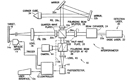
Fig. 1 is a block diagram of a presently preferred
embodiment of a laser ultrasonics materials analysis system
that is constructed and operated in accordance with this
10 invention. The system 10 generally operates by launching an
elastic wave within a target, sensing a varying surface
displacement of the target due to the elastic wave, and
then correlating the sensed displacement with a value of a
property or properties of interest. As employed herein an
elastic wave is intended to also encompass an acoustic
wave. Also as employed herein a target may be a solid, a
semi-solid, or a liquid.
A system controller 12, such as an embedded microprocessor
or an externally connected computer or workstation,
includes a user interface 12a that,includes, by example, a
touchscreen and/or a conventional keyboard and/or a
pointing device (e.g., mouse) in combination with a
graphical display device through which a user is enabled to
interact and direct the operation of the system 10. An
impulse laser 14 is controlled by the controller 14 to
provide an impulse beam 14a to the surface of an object,
hereafter referred to as a target 16 (the target forms no
part of the system 10, and is shown only for completeness) .
The impulse beam 14a causes a localized heating of the
target 16 and launches an elastic wave within the target as
described previously. A displacement of the surface of the
target 16 due to the elastic wave is detected by a
polarizing interferometer 18, and the detected displacement
is analyzed in accordance with a wavelet analysis
technique, described in detail below, in accordance with
CA 02224189 1997-12-09
WO 97/39308 PCT/US97/05982
7
this invention.
The interferometer 18 includes a detection laser assembly
20 which comprises a suitable laser 22, by example, a He-Ne
laser, a Nd:YAG laser, an argon laser, or a diode laser.
The selection of a particular laser 22 for use in the
system 10 is a function of the required power, coherence
length, wavelength, system compactness, and cost. Included
with the detection laser 20 can be a conventional Faraday
rotator (not shown) to prevent any reflected laser light
that returns from the target 16 from effecting the
performance of the laser 22. The output of the detection
laser assembly 20 is a source beam 20a.
The source beam 20a is provided to a beam expander 24. The
characteristics of the beam expander 24 directly impact the
light collecting power of the sensor system described
below. In general, the larger the beam diameter, the larger
the return speckle size, and thus the greater _is the
fraction of the total returned power that is available to
interference signal generation.
The beam expander 24 can be placed either before or after
a polarizing beam splitter 28 that is._described below.
Placing the beam expander 24 after the beam splitter 28 has
the advantage that the interferometer optics can be made
smaller and also independent of the expansion ratio of the
beam expander 24. However, placing the beam expander 24 at
this position requires that the detection or probe beam
(PB) 28b pass through the beam expander 24 twice. As a
result, the quality (cost) and alignment of the beam
expander 24 becomes important to the overall operation of
the system 10. As such, and although it is preferred to
place the beam expander 24 before the polarizing beam
splitter 28, as illustrated in Fig. 1, the teaching of this
invention is not so limited.
CA 02224189 1997-12-09
WO 97139308 PCT/L1S97/05982
8
The expanded source beam 24a next encounters a halfwave
plate 26 that is located before the polarizing beam
splitter 28. The halfwave plate 26 provides a mechanism for
setting a desired ratio for a reference beam (RB 28a) to
probe beam (PB 28b) intensity. Varying the rotation angle
of the halfwave plate 26 rotates the polarization of the
laser beam and, in combination with the operation of the
polarizing beam splitter 28 that is described next, thereby
controls the fraction of the beam going into the PB 28b and
into the RB 28a of the interferometer 18.
The halfwave plate 26 may be coupled to a mechanism, such
as a motor, for imparting a rotary motion to the halfwawe
plate 26. In this embodiment the controller 12
automatically monitors the signal returned from the target
16 and controllably rotates the halfwave plate 26, via
signal line 12b, so as to optimize the relative intensities
of the reference and probe beams. Alternately, this
function can be performed by a user who monitors a
graphical display provided by a camera 44 (described
below).
The rotated beam 26a that passes through the halfwave plate
26 is split into the RB 28a and PB 28b by the polarizing
beam splitter 28, with the RB 28a and PB 28b having
relative intensities set by the rotation imparted by the
halfwave plate 26. After the reference and probe beams 28a
and 28b leave the polarizing beam splitter 28 each passes
through an associated 1/4 wave retardation plate 30a and
30b, respectively. Plates 30a and 30b are aligned so that
both of the RB 28a and PB 28b are~circularly polarized.
The path length of the RB 28a is adjusted to reduce the
noise in the signal that is detected from a combined beam
(CB) 28c. The degree to which the lengths of the probe leg
and the reference leg are matched is a function of the
CA 02224189 1997-12-09
WO 97/39308 PCT/US97/05982
9
bandwidth of the laser 22, the fraction of the signal noise
that is attributed to any frequency j fitter of the laser 22 ,
and the impact of the length of the reference leg on the
overall compactness of the interferometer 18.
Included within the RB 28a leg are a plurality of folding
mirrors 32a and 32b and a corner cube reflector 34. It is
important to the operation of the interferometer 18 that
the reference leg return beam be at the same angle
(opposite direction) as the outgoing reference beam. This
important goal is achieved in a simple, compact, and
inexpensive manner using the corner cube 34. In contrast,
a simple mirror would require careful and precise
adjustment, and very high quality mounts all along the
reference path to maintain the alignment. In the presently
preferred embodiment of this invention these requirements
are eliminated by the use of the corner cube 34 (preferably
gold coated and hollow) which terminates the reference beam
path leg while preserving the polarization characteristics
of the RB 28a.
The PB 28b is focussed to a point on the target 16 using a
lens 36 that has a focal length equal to the distance to
the target 16. That portion of the PS 28b that reflects
from the surface of the target 16 is subsequently
collimated by the lens 36 as it travels back into the
interferometer 18.
The same prism (the polarizing beam splitter 28) that is
used to split the polarized beam 26a into the RB 28a and
the PB 28b is also is used to recombine the RB 28a and the
returned (reflected) portion of the PB 28b into a combined
beam (CB) 28c. Because the RB 28a and the PB 28b are
circularly polarized, and must pass back through the 1/4
wave plates 30a and Sob, respectively, they are again
linearly polarized, but at the opposite orientation than
CA 02224189 1997-12-09
WO 97/39308 PCT/US97/05982
their original linear polarizations. Because of this, the
CB 28c does not go back toward the laser 22, but instead is
directed into a signal detection portion of the
interferometer 18.
5
As was stated, after the RB 28a and the PB 28b are combined
they are both linearly polarized, but of the opposite
sense. In order to generate an interference signal
(detectable interference fringes), a polarizing prism or
10 beam splitter 38 oriented at 45° is used to select a
projection of the polarization axis of each of the RB 28a
and the PB 28b along a common axis. This results in two
combined beams whose interference signal is 180° out of
phase. Either or both of these beams can be used to provide
the signal necessary for process analysis. For example,
two photodetectors can be used for detecting two combined
beams. A combined beam focussing lens 40 is used to focus
the CB(s) 28c onto a radiation sensitive surface of one or
more photodetectors 42. The lens 38, in combination with an
aperture 41, can also be used to spatially block out light
other than that of the combined beams from impinging on the
photodetector 42.
The photodetector 42 may be provided in a number of
suitable forms, depending on performance characteristics.
Both conventional photomultiplier tubes and hybrid
photodiode/amplifiers are suitable embodiments for
detecting the light and dark pattern that results from the
interference of the RB 28a and the returned portion of the
PB 28b within the CB 28c. The output of the detector 42 is
provided to the controller 12 for wavelet analysis signal
processing in the manner described below.
An optional camera 44 is primarily used as a diagnostic
tool, i.e., the camera 44 useful for optimizing the
detected signal when an operator is setting up and
CA 02224189 1997-12-09
WO 97139308 PCT/US97105982
11
controlling the system l0. For example the camera 44, which
may be a conventional CCD device that provides an output to
a display monitor of the user interface 12a, provides
' visual feedback to the operator for best signal return,
which implies a best pointing angle to the target 16.
However, an automatic beam steering system can also perform
this function without operator intervention. The camera 44
may also be used for alignment of the signal and reference
beams. The camera 44 can also be employed to determine the
relative intensity of the reference and signal beams and,
based on the indicated intensities, the operator is enabled
to rotate the halfwave plate 26 to achieve an optimum
intensity distribution for optimum fringe contrast.
It should be realized that if the .camera 44 is eliminated
a second photodiode can be installed in its place. The use
of a second photodiode enables a square and add signal
processing technique to be used, as described in the above-
referenced U.S. Patent 5,286,313.
An application of the system l0, and in particular the
navel wavelet processing technique of this invention, is
illustrated in Fig. 2. This figure generally shows a rapid
thermal processing (RTP) system 110 which is used for the
thermal processing of a silicon wafer 112s. A heater module
114 surrounds a portion of a process chamber 116 which is
covered by a layer of thermal insulation 118. A lower
transfer chamber 120 enables the wafer 112 to be loaded
into and extracted from the process chamber 116. After
being loaded an elevator assembly 122 is used to raise and
lower the wafer 112 within the process chamber 116. A very
rapid heating (e. g., 50-100°/sec) of the wafer 112 occurs
during this process. Also shown in Fig. 2 are various
other system components such as a process controller 124,
an elevation motion controller 126, and an associated
motor/encoder 128 and amplifier 130 for raising and
CA 02224189 1997-12-09
WO 97/39308 PCT/US97/05982
12
lowering the elevator assembly 122. A pyrometer head 132
is connected via an optical fiber 134 to a pyrometer 136
for measuring, by emissivity, the temperature within the
process chamber 116. The pyrometer 136 is interfaced to
the process controller 124 to close the temperature control
loop.
In accordance with the invention the RTP system further
includes the laser ultrasonics materials analysis system l0
of this invention that employs wavelet transform analysis
processing. A laser head 11 is disposed so as to direct
the impulse beam 14a and the probe beam 28b onto a surface
of the wafer 112 during the thermal processing of the
wafer.
The temperature measurement of the wafer 112 occurs without
using the emissivity of the silicon wafer, which would be
difficult to accurately measure within the high ambient
temperature of the process chamber 116.
This is an important application of the invention as it
avoids processing errors which can result in the
destruction of the wafer 112. As larger wafers come into
use (e. g., 8" to 12" wafers) the expense of a single wafer,
which may have a very significant production cost
associated therewith, makes an accurate measurement of
wafer temperature an important goal.
Having thus described an embodiment of a laser ultrasonics
system that is suitable for use in practicing this
invention, and having also described one important but not
limiting application of the invention, a detailed
description is now made of the wavelet analysis processing
technique, in accordance with this invention, for
determining a characteristic, such as temperature, of a
material, such as the wafer 112 of Fig. 2.
CA 02224189 1997-12-09
WO 97/39308 PCT/US97/05982
13
The deficiencies of the conventional Fourier analysis
signal processing technique, when applied to short
duration, transient signals, was discussed previously.
These deficiencies can be at least partially overcome for
transient signals by processing with a windowed Fourier
transform. In this case, the basis function is a sine wave
which is localized within a decaying envelope that is moved
in the time domain. The presence of higher frequencies
l0 simply produce more cycles within~the same envelope. It
can be shown mathematically that since the window is fixed,
so are the time and frequency resolutions of this
technique. Limitations arise when the signal has both high
and low frequency components, where it is desirable to have
better time resolution at the higher frequencies.
This limitation can be overcome by using as basis functions
those which can be both translated and dilated. Such
window functions, denoted as affine wavelets or herein
simply as wavelets, have the special property that they
provide improved frequency resolution at low frequencies,
and improved time resolution at high frequencies.
In wavelet analysis, a class of functions denoted as a
"mother wavelet" is selected as the basis 'for decomposition
of the subject transient signal. Each single basis
function, or wavelet, is a translated and/or dilated
version of other wavelets, with the amplitude modulated to
maintain the total energy constant. If the entire series
of translated and dilated wavelets are transformed, the
result is a series of unit vectors forming a complete
basis. A wavelet can be visualized, therefore, by running
a unit vector through an inverse wavelet transformation.
Figs. 3a and 3b show wavelets generated in this manner for
two typical mother wavelet families: i.e., the Daubechies4
CA 02224189 1997-12-09
WO 97/39308 PCTJUS97/05982
14
and Daubechies20 families. Reference in this regard can be
had to Daubechies, I . , Ten Lectures on Wavelets, Society
for Industrial and Applied Mathematics, Philadelphia, PA,
1992, pp. 10-16.
The Daubechies4 wavelet of Fig. 3a was generated by a unit
vector in the 5th of 1024 components, while the
Daubechies20 wavelet of Fig. 3b was produced by a unit
vector in the 24th of 1024 components. Note that while a
wavelet function is continuous, it is not necessarily
differentiable everywhere, as seen in the Daubechies4
function. However, wavelets can still exactly recreate
some smooth functions.
The fact that a wavelet function can be compressed in the
time domain gives rise to the increased time resolution at
high frequency. Figs. 4a and 4b show a comparison of
windowed Fourier transform basis functions and wavelet
transform basis functions, respectively, at increasing
frequency. In particular, the waveforms on the right are
doubled in frequency over those on the left. As is
apparent, for the Fourier transform case (Fig. 4a) the
duration of the envelope remains the same while the number
of signal excursions doubles, while for the wavelet
transform case (Fig. 4b) the duration of the envelope is
decreased by a factor of two, while the number of signal
excursions remains the same. Reference in this regard may
be had to Livstone, M.M., "Wavelets: A Conceptual
Overview", MIT Industrial Liaison.Program Report 9-26-94,
Massachusetts Institute of Technology, Cambridge, MA, pp.
3-4.
One tradeoff in wavelet analysis is that time dilations of
the wavelets at higher frequencies reduces the f-:~quency
resolution, and vice versa. However, this mad- be an
acceptable compromise because short duration, low frequency
CA 02224189 1997-12-09
WO 97/39308 PCT/US97/05982
signals often cannot be well localized in the time domain.
As a result, in this case good frequency resolution is more
desirable than good temporal resolution. Conversely, high
frequency transients can be located accurately in time,
5 thereby making transient event detection feasible.
Wavelet transforms may be considered as either continuous
or discrete. In the continuous wavelet transform, the
parameters which control the translation and dilation vary
10 continuously over all real numbers. For discrete wavelet
transforms, these parameters take only discrete values
which, if chosen correctly, provide orthonormal wavelet
bases. The Discrete Wavelet Transform (DWT) allows rapid
computational techniques, similar in speed to the Fast
15 Fourier Transform, to be employed in decomposing a signal
into the superposition of wavelets with discrete time
dilation and translation constants. The results may be
expressed as a phase-plane map in which time and frequency
form the axes. The coefficient for each wavelet occupies
a certain range of position and frequency corresponding to
the resolutions of each parameter, producing a rectangular
area on the map. Constant wavelet energy considerations
dictate that the position and frequency resolutions are
inversely proportional for wavelet transforms. Thus, if the
frequency is very narrow (i.e., well-known), the position
must be broad, and vice-versa.
A third factor for each set of translation and dilation
parameters is also generated for representing the fraction
of energy of the original signal contained within a
particular wavelet. This third factor can be denoted by a
shading of the time-frequency domain on the two-dimensional
phase-plane map.
Fig. 5 shows the phase-plane map for a typical transient
signal at a fixed dilation constant using the Daubechies4
CA 02224189 1997-12-09
WO 97!39308 PCT/US97/05982
16
mother wavelets, while Fig. 6 shows an optimal phase-plane
map for the same signal. It should be noted that in Fig. 6
the time-frequency increments differ from those shown in
Fig. 5 because the combination of translated and dilated
versions of the mother wavelet, which best reproduces the
original signal, has been selected (thus optimizing the
phase-plane map). This set of (optimum) coefficients is
known as the best basis. The phase-plane map of Fig. 6
shows clearly how the Discrete Wavelet Transform provides
for multiscale analysis.
From Fig. 6, it can further be noted that most of the
energy of the measured trace is contained within just a few
coefficients. This means that virtually all of the
information of the original signal can be stored or
transmitted by relatively little data and, so long as the
mother wavelet family is known, the signal can be easily
reconstructed. The Discrete Wavelet Transform further
allows the wavelet coefficients to be used as figures of
merit for a given signal.
Having described the Discrete Wavelet Transform Analysis
technique in a general manner, the application of the DWT
Analysis technique to ultrasonic signals is now described
in detail.
When an ultrasonic response is generated in a material, the
measured signal, typically surface displacement, exhibits
transient behavior with a few oscillations that eventually
decay to zero. In certain cases these oscillations are
highly dispersive in the range of frequencies generated by
laser ultrasound. Fig. 7 shows a leading edge of a typical
laser-induced ultrasonic signal generated in a silicon
wafer, such as the wafer 112 illustrated in Fig. 2.
The inventors have realized that since the ultrasound
CA 02224189 1997-12-09
WO 97/39308 PCT/US97105982
17
generation clearly defines the start time of the signal,
and since there are few oscillations at any given
frequency, the ultrasound signal forms a suitable candidate
for wavelet analysis.
One benefit in using wavelet analysis on an ultrasound
signal is that a significant amount of information about
the signal is captured in a few dominant wavelet
coefficients. This feature is extremely useful when
analyzing several different ultrasound signals which vary
only slightly from one another, as would be the case if the
ultrasound were generated in a material with properties
that varied as the signals were being captured. Such
changes in frequency content are difficult to detect since
there are so few cycles to work with, and shifts in the
time domain can be small enough that they cannot be
reliably measured. Since wavelet analysis captures
information about the overall pattern of a signal, changes
from signal to signal that are difficult to resolve in the
time domain are measurable in the transformed phase-plane
space of a type illustrated in Figs. 5 and 6.
Example
The use of wavelet analysis for remote sensing of material
properties was performed using a laser ultrasound system
similar to that illustrated in Figs. 1 and 2. The target of
interest was a silicon semiconductor wafer, such as the
wafer 112 shown in Fig. 2. Temperature was selected as the
property of interest, although the teaching of this
invention is not limited only to the determination of
temperature. A sample wafer was heated in a furnace between
room temperature and 1000°F, and a reference temperature
measurement was provided by a thermocouple. Interferometric
signals output from the system 10 were digitized and
recorded. For each trace, 100 ultrasound signal events were
acquired, squared to eliminate interferometer phase
CA 02224189 1997-12-09
WO 97/39308 PCTIUS97/05982
18
artifacts, and averaged to produce the final ultrasonic
signal or trace. Each trace consisted of 1024 data points
taken over a 10 sec interval, starting 3 sec after the
impulse laser 14 was triggered. A commercially available
wavelet analysis program was used to analyze the traces,
specifically one known as Wavelet Packet Laboratory
Software, Version 1.02, available from Digital Diagnostic
Corporation of Hamden, CT. The teaching and practice of
this invention is not, however, limited only to the use of
this one commercially available wavelet software package.
The signals were processed using the same mother wavelet,
in this case the Vaidyanathan24 function. This function
was empirically chosen from among a number of suitable
other classes of mother wavelets. The selection was based
on the processing and subsequent qualitative observation of
wavelet coefficients for a representative laser ultrasonics
signal. Functions of various classes were tested, and the
chosen function was deemed to concentrate the signal energy
within a minimum number of coefficients at each dilation
level. Similarly, a constant dilation parameter was chosen
which best represented the sample signals, as indicated by
the localization of the total signal energy within the
fewest wavelet coefficients at that level of analysis. It
should be noted that the best basis combination of
translation and dilation parameters was not used because
the combination could change from signal to signal and,
therefore, a given coefficient could not necessarily be
used for consistent comparison.
Observing the coefficients from the seventh-level analysis,
where the wavelets were dilated in time by ( 1/2~) of the
mother wavelet, the energy content of the largest
coefficient was recorded for the first signal and compared
to the values for that same coefficient with each
subsequently analyzed signal (see Fig. 9). The variation of
CA 02224189 1997-12-09
WO 97/39308 PCT/US97/05982
19
this coefficient with temperature, corresponding to the
variation of the fractional signal energy contained within
that particular wavelet, was found to be approximately an
order of magnitude larger than any measurable variation in
the time domain.
That is, the energy found in at least one coefficient of
the wavelet is correlated with a property of interest of
the wafer, such as temperature, as will be shown in Fig. 9.
Other beneficial features of this technique are that lower
levels of signal-to-noise can be tolerated, because the
time-frequency localization can be tuned. That is, since
the technique analyzes the entire pattern of the signal and
can be locally optimized, relevant features can be
identified even with spurious information elsewhere in the
signal. For example, event detection can be accomplished
by increasing resolution in time preferentially for the
portion of the signal where the transient occurred. Other
portions of the signal could be optimized differently in
the time-frequency mapping to minimize the effect of that
noise and at the same time gain additional information
about the overall signal's features. Furthermore, the
results are already normalized, since it is the fractional
energy that is being measured. These properties are
particularly desirable for a laser ultrasonics application
where the energy deposition into specific ultrasonic
frequencies cannot be readily controlled.
Both theory and experimental data show that, for the
apparatus being used, a temperature resolution of about
10°F requires a resolution of 5 nanoseconds in conventional
time of flight measurements (signal-to-signal). However,
both noise and sample rate issues make this degree of
temporal resolution between signals difficult to achieve.
CA 02224189 1997-12-09
WO 97/39308 PCT/US97/05982
By example, Fig. 8 shows typical squared and averaged
ultrasound signals taken at 68°F and 1000°F for a <111>
silicon wafer. The variation in amplitude with time
(expressed in sampling points) indicates that there is
5 relatively little shift in the time domain of the
ultrasound response over this wide temperature range.
However, when the same data is analyzed using the wavelet
technique described above, the changes with temperature are
10 readily measured. In this regard Fig. 9 is a plot of the
energy content of the peak wavelet coefficient, at the
seventh level, versus temperature for the <111> silicon
wafer plotted in Fig. 8. A moriotonic decrease occurs
between room temperature and about 900°F, indicating a
15 sudden change in material properties at that temperature.
Accuracy of the temperature measurements in the region of
primary interest, between about 400°F and 900°F, was found
to average approximately ~20°F. This level of accuracy
resulted from the sample rate of the data acquisition
20 system recording the ultrasound trace. The uncertainty in
temperature measurement decreases when the sample rate is
increased. The measurements taken from a <100> silicon
wafer are also shown in Fig. 9.
From Fig. 9 it can be realized that not only can the
temperature be characterized but, assuming that temperature
was known a priori, some other material property of a
sample can be determined using the wavelet analysis
technique. By example, Fig. 9 makes it clear that one or
more properties characteristic of the sample's material
structure (e. g., presence of lattice defects, doping level,
or some other parameter affecting the elastic constants
other than temperature) can be identified and
distinguished.
Based on the foregoing it can be appreciated that wavelet
CA 02224189 1997-12-09
WO 97/39308 PCT/US97/05982
21
analysis can be employed to process laser ultrasound
signals obtained from a target with varying material
properties, such as temperature and crystal structure. The
technique is also applicable to the measurement of other
material properties and structure-related characteristics,
such as case depth, the ratio of austenite to martensite
(as well as other phase changes), and also thickness. By
measuring the energy content of at least one particular
wavelet coefficient for each signal processed with Discrete
Wavelet Transforms, a basis of comparison among the signals
is obtained which has a greatly improved resolution over
comparisons made only in the time domain (e.g., time-of-
flight).
Furthermore, the laser ultrasonics wavelet analysis
technique in accordance with this invention can be used
with signals with relatively poor,signal-to-noise ratios,
since it captures information about the overall pattern of
the signal, and is independent of the absolute amplitude of
the signals.
The teaching of this invention is not limited to only the
examples given above. For example, the laser ultrasonics
wavelet analysis technique of this invention can be used
for the measurement of surface properties. This is an
application wherein there is a modification of the surface
properties by some kind of surface treatment. The result
is a gradient of a particular material property from the
surface to the bulk of the material. An example of such a
process is the diffusion of carbon into steel during
carburization. The result is a surface hardened material
with carbon on the surface. The process is usually called
case hardening, and the depth of carbon penetration is
referred to as case depth. In some cases, the case depth
can be quite large, i.e., up to 0.25" and the carbon
gradient can start at high levels on the surface, for
CA 02224189 1997-12-09
WO 97/39308 PCT/US97/05982
22
example 5-10%, and drop to about 2% in the bulk. The
system 10 of Fig. 1 can be used to measure the depth of the
surface layer by analyzing the dispersion of the ultrasonic
waves using wavelets.
In a further application the system 10 can be used to
measure surface coatings. In this,application, the system
measures the properties of coatings, e.g., thickness,
integrity, uniformity, etc. This technique is similar to
10 the technique described immediately above, and differs most
significantly in that in this case there is a clear and
sharp interface between the coating and the substrate.
This method applies to any kind of coating, e.g., metal-on-
metal, paint-on-paint, paint-on-plastic, etc., so long as
an interface exists between a coating and another coating
or the bulk. In addition, the coating thickness can range
from microns to several millimeters or more. The frequency
of the ultrasonic wave can be adjusted according to the
thickness of the coating, e.g., higher frequency for
thinner coatings. Such frequency control can be achieved
by controlling the thickness of the impulse beam ring on
the target.
The system 10 using wavelet analysis is applicable to both
on-line and post-processing control. An example of on-line
control is the galvanization of steel, where zinc is
deposited on the surface of a thin strip. Measurement and
control of the properties and thickness of the zinc coating
are critical, and are accurately obtained in accordance
with the teachings of this invention.
While the invention has been particularly shown and
described with respect to preferred embodiments thereof, it
will be understood by those skilled in the art that changes
in form and details may be made therein without departing
from the scope and spirit of the invention. By example, the
CA 02224189 1997-12-09
WO 97/39308 PCT/US97/05982
23
teaching of this invention is not limited for use only with
the particular polarizing interferometer as shown in Fig.
1, nor is it limited for use only with an impulse laser for
generating the ultrasound signal, nor is it limited for use
only with semiconductor wafers, or silicon semiconductor
wafers in particular. That is, and by example,
semiconductor wafers comprised of Group II-VI and Group
III-V materials can be characterized as well using the
teachings of this invention.
ZO
It should therefore be realized that the teaching of this
invention should be given a scope commensurate with the
scope of the claims that follow.