Note: Descriptions are shown in the official language in which they were submitted.
CA 02224261 1997-12-09
LOW PHASE NOISE, HIGH Q,
HIGH GAIN AMPLIFIER IN AN INTEGRATED CIRCUIT
FIELD OF INVENTION
The present invention relates to: electronic oscillators
which act as the source of an oscillating electronic signal;
narrow bandwidth bandpass filters as are used in
communications systems; and the implementation of a low
phase noise, high Q, high gain amplifier in an integrated
circuit.
BACKGROUND OF THE INVENTION
El ectronic Osci11ators
Many electronic circuits require an oscillating source of
energy. Communications transmitters and receivers rely on
the purity and frequency accuracy of the oscillator to carry
their information or to receive information. If the signal
frequency is in error, the receiver may receive a degraded
signal or no signal at all. Similarly, if the purity of the
oscillation is poor (which is also referred to as the phase
noise of the oscillator), the desired signal may also
degrade or be totally corrupted.
CA 02224261 1997-12-09
The need for a pure, low phase noise oscillator affects the
cost of all communications systems to some extent, and in some
cases actually is the limiting factor in the system
performance. The cost of realizing a given low level of phase
noise in an oscillator directly affects whether a
communications system can be built for a reasonable cost.
To some extent, the difficulty in realizing a low phase noise
oscillator on the semiconductor also makes it difficult to
achieve low power consumption due to the need to amplify
signals to higher power levels for transmission on and off of
the integrated circuit (IC). More and more, communications
systems have a portable component, such as a wireless
telephone, pager, and the like. The power consumption of a
portable wireless device is very important as it directly
affects the life-span of the batteries, and the size and weight
of the batteries required to operate the device.
Narrow Band Fil ters
Communications systems transmit their signals over tightly
restricted radio frequency channels or 'bands'. The bands have
a certain 'bandwidth' which is directly related to the amount
of information which can be passed through the information
channel. Due to the relative scarcity of radio frequency bands
and the limited ability of electronic instruments to use
extremely high bands, most communications systems are forced
CA 02224261 1997-12-09
to operate in close proximity to other bands. From the point
of view of the communications user, all other signals can be
regarded as interfering signals. Hence, communications systems
attempt to use the band of interest while excluding
interference from all other bands.
Communications systems all use some form of band limiting
filter to allow the desired information to pass while excluding
all other interference. The ability to build the band limiting
filter such that it matches exactly the information sent
usually affects the ultimate performance of the system, and the
cost of its realization.
Band limiting is done with filters. While some filtering can
be done digitally, due to the limitation of quantizers to
digitize very large bands, and the high power consumption of
such techniques, most communications systems rely on some form
of analog filtering. An analog filter generally consumes no
power, and loses very little in its implementation. The problem
with analog filters is that they are limited in their ability
to attain ideal filters by the quality or 'Q' of the
components. This is the same limitation which applies to the
quality of electronic oscillators discussed above. As a
result, the Q of the filter components affects the ability to
realize better communications systems.
CA 02224261 1997-12-09
In general, low loss passive filters are built with
combinations of lumped elements known as inductors and
capacitors, or with equivalent distributed resonant structures
such as ceramics, crystals, resonant transmission lines, and
the like, or with hybrid lumped element structures with
partially resonant structures, such as shortened transmission
lines with capacitors or inductors added.
At radio frequencies, high quality inductors are much more
difficult to build than high quality capacitors. In general,
inductors useful at radio frequencies are also much larger than
capacitors. As a result the inductors tend to limit the radio
filter design (or the low phase noise oscillator design).
Because the integrated circuit is very small, and necessarily
made of semiconducting materials, it is very difficult to build
a low loss inductor on an integrated circuit. As a result,
filters requiring inductors or oscillators tend to be of a
lower quality that those which can be achieved with components
built external to the semiconductor (off-chip). This directly
affects the cost of manufacturing a communications system.
Hence, the filter is limited for very similar reasons to the
limitations on the low phase noise oscillator.
Historical Solutions
Many techniques have been devised to make oscillators both
accurate in frequency and having low phase noise. Most
CA 02224261 1997-12-09
techniques require complex circuits and shielding which is not
readily integrable into an integrated semiconductor solution.
As a result pure oscillators with low phase noise are not
generally realizable in integrated circuit form without the aid
of many external components, which are directly used to control
the phase noise of the oscillator.
Traditionally, a separate external oscillator circuit is used
to provide the low phase noise source. This solution works
well but is more expensive than an integrated solution. More
recently, a common approach is to implement a partial solution
whereby a resonant circuit with a high quality factor (Q) is
used external to the semiconductor and only the active
transistors are on the semiconductor. This solution still
suffers from the expense of the external resonator. Also, if
the frequency is high, it can be very difficult to properly
couple the internal circuit to the external resonator. This
is especially true if low cost plastic packages are used with
high pin counts.
Many recent attempts to build resonators directly on the
semiconductor or immediately above the semiconductor using
lithographic or other techniques have met with very limited
success, and the resonators achieved are of comparatively poor
quality, for example Q's of from 5 to 20.
CA 02224261 1997-12-09
Thermal amplifiers have been implemented in a very crude and
uncontrolled form for many years in the form of a device known
as a super regenerative receiver. This device, due to its lack
of control, alternates itself from completely turned off,
through the thermal amplifier state, into an oscillating state.
This type of device benefits from the momentary high Q achieved
as it passes through the optimum gain state. The Q of the
device varies over an extreme range as it passes from off to
oscillating. As a result, the device must be pulsed on and
off. The super regenerative receiver also benefits from the
fact that it has very low power consumption. Super regenerative
receivers have typically only been used in relatively simple
applications, such as garage door openers, due to their crude
control mechanisms. They can achieve very high sensitivity but
are difficult to tune and are highly non-linear. This has made
the super regenerative receiver a poorly understood device. As
a result of these factors, super regenerative receivers have
seen limited usefulness in more general high performance
communications applications. Super regenerative receivers also
require a stabilizing device such as a high Q filter or
resonator. This increases their cost and limits the ability
to integrate this type of device on an integrated circuit.
SU~ RY OF THE INrVENTION
This invention addresses a technique to produce a low phase
noise, high Q, high gain amplifier which may be realized in a
CA 02224261 1997-12-09
low power integrated circuit form without the need for an
external high quality resonator. This type of application is
sometimes called an active filter.
The high Q high gain amplifier may be used as the source of a
low phase noise electronic signal, despite the fact that it is
not technically an oscillator. It is more correctly an
amplifier. For the purposes of discussion the invention will
be referred to as the 'KT amplifier' due to the important role
of thermal noise played in the invention.
The KT amplifier may have a signal as an input, in which case
it is used as an active filter with very high Q and very high
gain. The KT amplifier may be used with no external source, but
may use its own thermal noise as its input to produce a high
quality low phase noise sinusoidal signal. In this case, the
device performs the identical function to an oscillator in a
communications system.
The KT amplifier invention, in either of its forms as a source
or as an active filter, can be realized on an integrated
circuit at radio frequencies without the need for high quality
lumped or distributed elements, but simply with a high quality
low cost reference such as might be generated by a fundamental
mode AT cut crystal based device.
CA 02224261 1997-12-09
As a result of this invention, it will be possible to build
communications systems at lower cost, with high performance,
and with very low power consumption. The Q of the oscillator
or filter resonator is one measure of the quality of the
device. Typical on-chip resonators today have Q's of from 5
to 20 at frequency ranges of use to radio devices. This
invention presents a technique which allows Q's of from 10 to
over 100 times higher than is common using on chip resonators.
Other advantages, objects and features of the present invention
will be readily apparent to those skilled in the art from a
review of the following detailed descriptions of a preferred
embodiment in conjunction with the accompanying drawings and
claims.
BRIEF DESCRIPTION OF THE DRAWINGS
The embodiments of the invention will now be described with
reference to the accompanying drawings, in which:
Figure 1 is the KT amplifier modelled as a classic feedback
control system;
Figure 2 is a simplified KT amplifier;
Figure 3 is a general form of an embodiment of the invention;
and
CA 02224261 1997-12-09
Figure 4 is an example of a more detailed embodiment of the KT
amplifier invention.
DETAILED DESCRIPTION OF THE INVENTION
This invention makes use of an amplitude feedback control loop
to control the output power level of the KT amplifier. The KT
amplifier is analyzed as a classical feedback control system,
as shown in Figure 1. As will be shown later, some important
additions to the amplitude and frequency feedback control are
required to realize a practical form of the invention on an
integrated circuit. In its most general sense, the input
signal, Vin, is the input referred thermal noise of the
amplifier plus any external source of energy. In its
realization as a source the external signal, Vext, is not
required.
Vin = KTFB + Fin
where:
K is Boltzman's constant,
T, is the absolute temperature in degrees Kelvin,
B is the 3 dB bandwidth of the thermal noise in the steady
state closed loop measured in Hertz (Hz),
Vext is the external input signal,
and
F is the noise figure of the amplifier.
The output signal is the output of the KT amplifier.
CA 02224261 1997-12-09
Vo = VinG
where G is the closed loop gain, if the open loop gain is less
than unity. If the open loop gain, AH, is greater than unity
the device will oscillate and the output will increase until
it is limited by the saturation of the amplifier.
For AH<1, the steady state closed loop gain of the system is:
Vo/Vin = A/(1-AH)
For illustration purposes only, we can assume that the gain of
H= 1 and is realized by a simple delay T. This is not
necessary for the invention but makes the analysis simpler for
illustration purposes. The KT amplifier may be redrawn as
shown in Figure 2. In this case the steady state gain at
frequency f is given by:
Vo/Vin = A/(1-Acos(2piTf)), where Pi = 3.14159.
This is a tuned amplifier with gain which approaches infinity
for A = 1-E and E approaching 0. This high gain state occurs
only at frequencies fo, where
fo = n/2piT and n=integer.
In its preferred state the invention would reduce the open loop
gain at all integer multiples except the preferred frequency.
The most easily realized preferred frequency is the case where
n=1. In this case the undesired DC case would be limited for
CA 02224261 1997-12-09
example by AC coupling and the undesired integers >1 could be
limited by the amplifier bandwidth or by any other technique.
In this case, for Ec<l, the gain is given approximately by:
G(fo) = -l/E
where the negative sign simply indicates a phase inversion at
the output relative to the input.
The Q of the KT amplifier is given by:
Q=fo/B
where B is the 3 dB bandwidth of the output signal. Hence, the
gain at fo+/-B/2 is given by:
Gain(fo+/-B/2) = Gain(fo)/(2 .5)
It can easily be shown for this example that for high gains,
i.e. E<<l, that the Q may be expressed approximately as:
Q=3.45/EAo.5
Similarly, the 3 dB bandwidth of the output signal, B, can be
shown to be approximately:
B=foE Ø5/3.45
As an example:
Let the open loop gain be
AH = l-E where E=le-5, for n=l and AH far from unity for n not
equal to 1,
and assume the noise figure F is:
f=5 ds,
CA 02224261 1997-12-09
Thermal noise
KT = -174dBm/Hz,
Input signal Vin = 0
T = 2nsec
The output frequency fo would be
fO 1/T = 500 MHz,
the output gain would be
G(fo) = -201Og(E) = 100 dB
The output Q would be:
Q = 3.45/(le-4)A.5 = 1091
The 3 dB bandwidth would be given by:
B = fo/Q = 500Mhz/1090 = 459 kHz
The output power in a 50 ohm system would be:
Po = KTBFG(fo) = -174+101Og(459e3)+5+100 = -12 dBm (or 152mV
peak-to-peak (mVpp) in 50 Ohms)
The noise floor of the source will simply be KTFA. (Note,
normally H will have some losses, hence A will compensate by
being slightly greater than 1.) The phase noise of the
oscillator at any given frequency can then be easily calculated
using Lessons model.
The same example device can be used to amplify signals inside
of its 3 dB bandwidth. Within the limitations of the KT
amplifier output swing the signal will be amplified by 100 dB.
Hence, to achieve an output signal-to-noise ratio (SNR) of
12
CA 02224261 1997-12-09
lOdB, it would be necessary to inject a signal of input power,
Pin, where
Pin = Po-G(fO) +SNR = -12 -100 +10= -102 dBm
Hence, in this example, the input sensitivity of the KT
amplifier is -102dBm for an output SNR of +lOdB and the signal
bandwidth could be up to 459kHz.
The output signal power of the amplifier, Po, would be just,
Po = Pi + 100 = -102 +100 = -2 dBm (or 500 mVpp in 500hms)
It should be noted that as the input signal is increased
quickly relative to the bandwidth of the amplitude control
loop, then the output signal increases linearly until the
amplifier A starts to saturate. We can refer to the difference
between the minimum useful input signal at a given SNR, to
maximum signal before any significant change in closed loop
gain, as the linear dynamic range. At end of the linear dynamic
range the loop will have gain of less than unity and the Q will
start to drop, i.e. the noise bandwidth will start to increase.
This will be compensated for, however, by the fact that the
signal is growing, hence the SNR will be maintained at a useful
level over a much wider range. It should be noted that this
type of amplifier would not be useful to demodulate a small
input signal in the presence of a larger input signal in the
same band, as the larger input signal will reduce the Q and the
gain of the amplifier. As a result, all practical amplifier
applications must use some combination of traditional
13
CA 02224261 1997-12-09
pre-filtering or feedback filtering to keep the loop from being
captured by interfering signals. The extent of the traditional
filtering required would depend upon the application. This
limits the usefulness of the KT amplifier in some
communications systems, but in no way limits its general
usefulness as a signal source.
A practical embodiment of the invention is shown in Figure 3.
The classical feedback loop requires the addition of:
a) A gain controlled amplifier, possibly with both fine gain
adjust and a crude or discrete gain adjust. The fine gain
adjust is such that it has a very limited gain adjust over a
large control voltage. This is very important to allow the
amplifier to reach the tight levels of gain controls required
for the invention. The discrete gain adjust will be used to
place the amplifier at a gain within the control range of the
fine gain adjust. The discrete gain adjusts will be noise
immune as they are of a switched nature and do not rely on a
low noise analog control. The need for the discrete gain
adjust and the number of discrete levels required will depend
upon the precision and the Q levels to be achieved and on the
precision of the IC processes being used.
b) A method to measure the output signal strength of the
amplifier, called here the received signal strength indicator
circuit (RSSI).
14
CA 02224261 1997-12-09
c) A method to limit the bandwidth of the RSSI output. This
filter will limit noise and upper order signal harmonics
generated by the RSSI. The bandwidth of this filter will
depend upon the application, as either a signal source (low
noise oscillator) or as an active filter with communications
signal as the input to the KT amplifier.
d) A method to generate a reference voltage, VREF.
e) A method to produce an amplitude error signal, Ea, by
subtracting the output of the band-limited RSSI signal from the
VREF signal.
f) A method to integrate the error signal Ea with a high gain
integrator.
g) The output of the integrator is appropriately level
shifted and scaled so as to control the fine gain adjust of the
amplifier, A.
h) A method to measure the output in discrete steps such as
an A/D converter, to allow the gain to be adjusted in discrete
steps to within the fine adjust range where the integrator
takes over.
The frequency of the signal being generated or filtered is
controlled by the delay T. In an IC this delay cannot be
CA 02224261 1997-12-09
achieved accurately without some form of feedback. The
preferred method of the invention is to limit the range of
delays through some physical means, which will limit the range
of possible oscillation frequencies. The practical limits must
take into account the tolerances achievable on a given IC
process. +/- 20~ of the desired delay is a commonly achievable
accuracy with out special means.
Depending upon the application the fine frequency adjust
required for the invention may be achieved in a number of
different forms. If a low phase noise signal source is desired
then a crystal oscillator reference should be used with a phase
locked loop (PLL). This type of circuitry is readily
achievable in IC form with only the crystal itself and portions
of the PLL low pass loop filter required external to the IC.
In the simplest form the reference may be chosen as a fixed
integer sub-multiple of the desired output frequency. In a more
advanced variation of the invention the reference may be
operated in a variable PLL which can achieve many sub-multiple
division ratios, including rational numbers such as might be
achieved with a fractional-N synthesizer based PLL for example.
For the purpose of simplicity, and without loss of generality,
we will simply describe the integer sub-multiple example.
16
CA 02224261 1997-12-09
If the desired output frequency, fo, and the reference
frequency fref, are related by the division ratio, n, as
follows,
fref = fo/N,
Then within the bandwidth of the PLL the phase noise of the
output source offset by some frequency, f, from its central
spectral line, No(f), will not be that predicted by the Q of
the free running KT amplifier, Nkt(f), but that of the
reference, Nref(f), multiplied up to the output frequency, that
is within the loop bandwidth:
No(f) = Nref(f) + 2010g(N) expressed in dBc/Hz offset from the
center frequency by f Hz.
Outside of the bandwidth of the PLL the KT amplifier output
phase noise will simply be that of the free running KT
amplifier. Due to the high quality of the free running phase
noise spectrum of the KT amplifier, a given application can use
a very narrow PLL loop bandwidth, when compared with the loop
bandwidth of a traditional noisy oscillator. Due to the
extreme problems which can be caused by high loop bandwidths,
and high free running phase noise of the oscillator, in many
applications the result is that the KT amplifier would be the
only solution for an on chip low phase noise source.
If the in-close phase noise of the KT amplifier is not a
requirement for the application as may be the case say for some
17
CA 02224261 1997-12-09
less demanding applications then, the frequency control loop
may be simplified to a simple frequency locked loop (FLL).
This type of loop simply counts the output frequency over a
long period of time, and compares the result with a similar
count of the reference frequency over the same period of time.
The comparison is used in its simplest form to decide to adjust
the delay T up or down to achieve the correct output frequency.
The tolerance of the output frequency will be approximately the
accuracy of the crystal in PPM, and the reciprocal of the count
interval, which ever is greater. Typically a low noise fine
frequency control loop can be built with a charge pump on an
IC which pumps up or down to adjust the frequency. The fine
phase adjust can be achieved in a number of ways. One method
is to use a voltage variable capacitance, such as a bipolar
transistor junction in back bias, as the delay adjust element.
Similar to the amplitude control loop the delay can be
implemented with fine and crude adjustments, with the crude
steps adjusted by discrete means and the fine adjust controlled
by means of a large voltage to control a fine delay adjust.
This is the most noise immune approach. Again requirement for
the crude adjust, and the number of levels of crude adjust will
be determined by the precision of the application and the
tolerances of the IC process used.
18
CA 02224261 1997-12-09
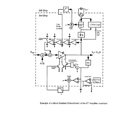
A more detailed embodiment of the invention is shown in
Figure 4 with examples of realizable approaches on an IC
process.
Important aspects of the invention are as follows:
a) A method to adjust the gain of the closed loop to a high
level of tolerance
this requires as a minimum
- a variable gain amplifier
- a method to produce a signal, Vm, related to the
signal strength of the output signal
- method to filter the noise bandwidth of the signal
Vm
- a method to generate a reference voltage
- a method to compare the reference voltage with the
filtered Vm to produce an error signal Er
- a method to integrate Er
- a method to create an amplitude control signal, Ac,
based upon the integrated value of Er
- a method to adjust the gain of the amplifier, A,
based upon the value of the control signal Ac.
b) A method to adjust the frequency or the phase of the KT
amplifier output to a high degree of tolerance
the frequency control of the KT amplifier requires as a
minimum
19
CA 02224261 1997-12-09
- a method to divide the output signal to a lower
frequency
- a method to count the lower frequency over an
interval of time, Tc
- a method to compare the result of the count with the
expected number of counts of the reference over the
same period of time,
- a method to limit the bandwidth of the comparison
- a method to adjust the delay of the KT amplifier
loop based upon the results of the band-limited
comparison.
All of the above adjusts may need to be done in crude discrete
steps and in fine vernier steps depending upon the application.
This does not change the generality of the invention.
Numerous modifications, variations and adaptations may be made
to the particular embodiments of the invention described above
without departing from the scope of the invention, which is
defined in the claims.