Note: Descriptions are shown in the official language in which they were submitted.
CA 02224606 1997-12-11
1
PATENT
A DISTRIBUTED BUFFERING SYSTEM
FOR ATM SWITCHES
BACKGROUND OF THE INVENTION
This invention relates to communication networks
and, in particular, to switches in an asynchronous transfer
mode (ATM) network.
In a communication network, units of data must be
routed between different points of the network through
switches. In ATM networks, traffic streams of mixed types of
information are carried according to the concept of "bandwidth
on demand." The data units, ATM cells, are transferred in
accordance with. the varying requirements of each ATM cell.
Data units which are time critical are given priority in
network routing. Data units which are information critical
are given priority against cell loss. This ability to handle
video, voice, computer data and other information has led to
the wide acceptance of ATM as a prospective network standard.
An ATM network switch must route information
reliably with minimum delay and loss, but the wide variation
in requirements in ATM networks creates heavy demands upon the
ATM switch. In particular, previous designs have placed a
buffer at each output port of the ATM switch to store cells
arriving faster than the output port can transmit to its
output channel. The buffers created operational tolerance to
differing demands on the ATM switch to avoid losing cells. A
variation of this concept has been to place a storage buffer
which is commonly used by all the output ports of the ATM
switch.
These different designs have various shortcomings,
including complexity, high cost, and impediments to
configuration changes. Another shortcoming is that the simple
buffering at the output port set a limit on the amount of
buffering available to the output port. However, the
probability of congestion at an output port is directly
related to the number of input ports feeding the output port.
CA 02224606 2002-08-22
-2-
As more input port ports are added to the ATM switch, the
probability of overwhelming an output buffer increases.
For the design with a common buffer shared by all the
output ports, performance is often not better. If enough
data arrives at an output port, a large fraction of the
common buffer is occupied by the cells destined for the
output port and is unavailable to the other output ports.
This can cause problems, particularly in networks with
multiple servers.
The present invention solves or substantially mitigates
these problems with an ATM switch which has buffering
distributed for higher performance and which allows for
greater modularization of design.
SUMMARY OF THE INVENTION
An ATM switch for transferring cells from a plurality of
input channels to a plurality of output channels, said
switch comprising a plurality of input ports, each input
port connected to one of said input channels and operable
to receive cells from said one input channel, said input
port having an input buffer operable to hold cells when
said cells arrive faster from said input channel than
said input port transmits; a plurality of output ports,
each output port connected to one of said output channels
and operable to transmit cells to said one output
channel, said output port having an output buffer
operable to hold cells when said cells arrive faster from
said input ports than said output port transmits; a
switch block connected between
CA 02224606 2002-03-15
-2A-
each one of said input ports and each one of said output
ports, said switch block being operable to convey cells
from said input ports to said output ports, said switch
block having a plurality of interconnected switch
elements, each switch element having a plurality of input
terminals, a plurality of output terminals and a switch
bus, each input terminal having an input buffer operable
to hold cells received by said input terminal, each
output terminal having an output buffer operable to hold
cells to be transmitted by said output terminal, and said
switch bus being operable to transmit cells from said
input terminal to said output terminals; and a
backpressure signal circuit connected between each output
buffer of each output port and each input buffer of each
input port, said backpressure signal circuit being
operable to send a signal from a congested output buffer
to input port buffers which had immediately transmitted a
cell to said output buffer so that said input port
buffers cease transmission so that cells destined for
said output buffer are stored in said input port buffers.
BRIEF DESCRIPTION OF THE DRAWINGS
The invention may be better understood by reference to the
following detailed description in connection with the
accompanying drawings:
CA 02224606 1997-12-11
3
Fig. 1 is a representation of the distributed
buffering of an ATM switch according to the present invention;
Fig. 2 is a block diagram of the general
organization of an ATM switch according to an embodiment of
the present invention;
Fig. 3 is a block diagram of the switch fabric of
the ATM switch of Fig. 2;
Fig. 4 is a block diagram of the elements of a
switch routing element of the switch fabric of Fig. 3;
Fig. 5 illustrates the mapping of routing tag fields
to switch routing elements in the switch fabric of Fig. 3;
Fig. 6A illustrates the cell path of a unicast
connection in the switch fabric for exemplary values in the
routing tag field; and Fig. 6B illustrates the cell path of a
multicast connection in the switch fabric for exemplary values
in the routing tag field; and
Fig. 7 is a representative diagram of the
backpressure control block of the switching routing element of
Fig. 5.
. DETAILED DESCRIPTION OF SPECIFIC EMBODIMENTS
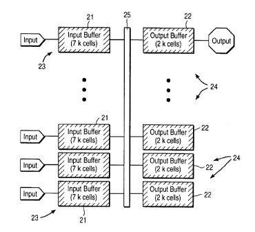
The general organization of an ATM switch and its
distributed buffering system according to one embodiment of
the present invention is illustrated in Fig. 1. Each input
channel is connected through an input port 23 with an input
buffer 21 and each output channel is connected through an
output port 24 with an output buffer 22. The input buffers 21
and output buffers 22 are connected to a switch block 25 by
which incoming ATM cells are routed from an input buffer 21 to
the proper output buffer 22 (and output port). Cells enter
the ATM switch though one of the input ports 23. If the
switch block 25 is not congested, cells are transferred
through the switch block 25 to one or more output ports 24.
If the output port 24 is not already transmitting a cell, then
the arriving cell proceeds directly through the output port 24
to the connected output channel. Otherwise, the cell is held
in the output buffer 22 until the output port 24 is ready to
transmit the cell to the output channel.
CA 02224606 1997-12-11
4
Cells from multiple input ports 23 can converge upon
the same destination output port 24 to cause its output buffer
22 to become congested and overflow. A backpressure signal
circuit (not shown in this drawing) is operative at this
point. If an input buffer 21 transmits a cell to a congested
output buffer 22, the backpressure signal circuit sends a halt
signal to that input buffer 21 so that port 23 stops sending
cells. Cells arriving from the input channel of that port 23
are stored in the input buffer 21 of that port 23. When the
congested output buffer 22 empties below a predetermined
threshold, i.e., the buffer 22 is no longer congested, the
backpressure signal circuit removes the halt signal to the
input buffers 21 previously halted to resume transmission to
the switch block 25.
With this distributed buffering system, the input
buffers 21 can jointly store cells destined for a common
output port 24 with a congested output buffer 22. This allows
the amount of buffering available for each output port 24 to
grow with the number of input ports 22, the source of
congestion.
The details of a particular embodiment of an ATM
switch according to the present invention are illustrated in
Fig. 2. The input ports 23 and output ports 24 are integrated
into line interface modules 20, each of which is connected to
several input and output channels. While a time-division
multiplexed bus could also be used for the switch block 25, a
switch fabric 10 having multiple switching elements is
considered highly suited for the ATM switch described below.
The ATM cells traveling through an ATM network enter
through a line interface module 20, route through the switch
fabric 10, and exit to the network through another module 20.
The switch also has a controller unit 16 which communicates
with the modules 20 and switch fabric 10 through a control bus
15. The controller unit 16 configures and monitors the line
interface modules 20 and the switch fabric 10.
The controller unit 16 provides all call access
control functions, including call setup, maintenance, and
teardown, and processes the information measured by the line
CA 02224606 1997-12-11
interface modules 20 to maintain connection and link
statistics for network management. Operationally, signaling
and management cells are transmitted to and from the
controller unit 16. These cells are received by the unit 16
5 after they pass through the switch fabric 10 to an output
module 20. The signaling and management cells are removed
from the output module 20 and sent to the controller unit 16
through the control bus 15. The controller unit 16 transmits
signaling and management cells to the network by sending these
cells to an input module 20 by the bus 15. The cells are
routed through the fabric 10 to an output module 20 and
transmitted to the network.
By passing such control information for the
controller unit 16 through the switch fabric 10 first before
the information reaches the controller unit 16, or before the
information generated by the controller unit 16 leaves the
switch, multiple controller units 16 can each monitor a fixed
number of line interface modules 20 with call control and
network management messages passed through a central processor
when the switch architecture is expanded to a larger number of
ports. This modularity in control and network management
design permits for ready expansion of the ATM switch. Control
and management processing capacity, i.e., the control units
16, is added with more switching capacity, i.e., the line
interface modules 20.
The line interface modules 20 support all the by-
line and by-connection functions, the physical layer link
termination, translation of ATM cell header information into
routing tags for use by the fabric 10, traffic policing, cell
rate decoupling, including the insertion and deletion of
unassigned cells. Each module 20 also measures cell loss,
cells tagged, cells passed and the number of cells dropped for
each connection. On the other hand, the switch fabric 10,
which routes cells received from a module 20 to one or more
modules 20, maintains queue-level statistics on congestion by
the measurement of the number of cells during which
backpressure (described below) is applied, and the amount of
cell loss.
CA 02224606 1997-12-11
6
Each line interface module 20 form four input ports
23 and four output ports 24 of the ATM switch, with each input
buffer 21 connected to a communication line from which ATM
cells are received. Each output buffer 22 of an output port
24 is connected to a communication line to which cells are
transmitted.
The large amount of buffering capability of the ATM
switch is distributed between the line interface modules 20
operating as an input module and output module, and some
buffering in the switch fabric 10. As indicated in Fig. 1,
each input buffer 21 has the capacity to hold 7,000 cells and
each output buffer 22 has the capacity to hold 2,000 cells for
the particular ATM switch described. The buffering minimizes
cell loss for bursty traffic, while avoiding delay for time-
critical data. The switch drops cells on a per-connection
basis, rather than on cell priority level. The senders) of
the congestion-causing data is penalized, rather than the
other users of the ATM switch.
Though much smaller than the input and output
buffers, the buffering in the switch fabric 10 allows cells to
continue to move through the switch fabric 10 when there is
contention between cells for the same output port. The large
buffering in the modules 20 operate when there is congestion
caused by bursts of cells from different connections headed
for the same destination (port).
The switch fabric 10 is detailed in Fig. 3. The
fabric 10 is a 16-port buffered Benes interconnection network
with 4X4 switch routing elements 11. That is, each switch
routing element 11 has 4 input ports and 4 output ports. As
shown in Fig. 3, the leftmost column of elements 11 are each
connected to the input ports of a line interface module 20.
The four output ports of each of these elements 11 are, in
turn, connected to input ports of the middle column of
elements 11. The output ports of the middle column of
elements 11 are connected to the input ports of the rightmost
column of switch routing elements 11. The output ports of
these elements are connected to the output ports of the line
interface modules 20.
CA 02224606 1997-12-11
7
An element 11 routes each individual ATM cell from
one of its input ports to the proper output ports) by the
bits within the routing tag of the cell header. A fabric
control bus 17, which is directly connected to the control bus
15, allows the controller unit 16 to program the elements 11
and to read their status. A fabric base clock (FBCLK) signal
sets the rate at which the cells are acted upon by the
elements 11 for transfer through the switch fabric 10 from
element 11 to element 11. This determines the internal link
rate of the fabric 10.
The elements of each switch routing element 11, a
fully 4X4 non-blocking element, is shown in Fig. 4. Each
element 11 has four sync buffers 12, each connected to an
output port of a line interface module 20 or of another switch
routing element 11. The sync buffers 12 are connected to
switch bus 13, which is in turn connected to four output
selection blocks 18. Each output selection block 18 is
capable of holding 32 cells, while a sync buffer 12 can hold 2
cells. Hence each switch routing element 11 can hold up to
136 cells at a time. To handle congestion problems, the
switch routing element 14 has a backpressure control block 14
which can receive backpressure signals from each one of the
output selection blocks 18 and pass on the backpressure
signals to each one of the sync buffers 12, as described
below. A control interface block 19 handles control and
signaling functions for the element 11 through a control port
which is connected to the control fabric bus 17.
Cells are clocked into a sync buffer 12 at the rate
the cells are transmitted into the element 11. The cells from
the four sync buffers 12 are multiplexed through the switch
bus 13. The output selection blocks 18 read the routing tags
for each cell, and route the cells towards their respective
output ports. Each output selection block 18 reads either a
multicast routing field ('M' field) or unicast routing field
('S' field) in the cell header. The mapping of switch routing
element position to the routing tag field is shown in Fig. 5.
The first stage of the switch routing elements 11 in
the switch fabric 10 are all programmed to read the S field.
CA 02224606 1997-12-11
8
These switch routing elements 11 can use the same routing tag
field, as the cells which pass through them all come from
different sources. Furthermore, the value of the S field
uniquely determines to which second stage switch routing
elements 11 the cell will go. The cells are routed to the
switching element output as described in the table below.
S field value Output Port
0 0
1 1
2 2
3 3
A cell with the value '1' in the S field is routed to port 1
by a switch routing element 11 in the first stage. This cell
travels to the switch routing element '21', regardless of
which switch routing element routed the cell in that
direction.
The second stage of switch routing elements 11 also
use the same field. However, these switch routing elements 11
must be capable of routing the cells to multiple switch
routing elements 11 in the third stage so that these switch
routing elements are programmed to read an M (or multicast)
field in the routing tag, i.e., the field M1 in the routing
tag illustrated in Fig. 5.
In an M field, a value of '1' in each individual bit
of the field indicates to the output selection block 18 that
the cell is destined for its output port. The mapping is as
shown below:
M field
bit 3 bit 2 bit 1 bit 0
Port 0
Port 1
Port 2
Port 3
Thus if a cell with the bit pattern, '1011' in the M1 field,
arrives at a switching element 11 in the second stage of the
fabric 10, the output selection block 18 for ports '0', '1',
CA 02224606 1997-12-11
9
and '3' copy the cell from the switching bus into the buffer
within the output selection block 18. The copies of the cell
are eventually transmitted through the output ports '0', '1'
and '3' to the switching elements '30' , '31' and '33' in the
third, and last, stage of the switch fabric 10.
The switch routing elements 11 in the third stage of
the switch fabric 10 route cells directly to the outputs of
the switch fabric 10 itself. For multicasting capability,
these switching elements 11 are programmed to use the 'M'
(multicast) fields in the routing tags of the cell headers.
Furthermore, it is desirable to be able to route only the
cells to any combinations of the output ports. Since each of
the last stage switching elements 11 are only connected to
four of the switch fabric output ports, each of the third
stage switching elements 11 must have a distinct 'M' field in
the routing stage. Thus the switching elements '30', '31' '32'
and '33' are programmed to read fields 'M2', 'M3', 'M4', and
'M5', respectively. The operation of these fields is exactly
the same as for the 'M1' field.
Figs. 6A and 6B illustrate the routing path through
the switch fabric 10 for a unicast connection, and for a
multicast connection, respectively, for exemplary routing
tags. The darkened lines between the switch routing elements
11 of the various stages illustrate the routing of the cell.
Cells are lost in transmission if the destination
buffer of the cells has overfilled so that it can no longer
store more cells. To lessen these occurrences, the buffers in
the ATM switch cooperate through a backpressure signal
circuit. A backpressure signal, an Overfill signal, is
applied by a destination buffer to any source, either a line
interface module 20 or a switch routing element 11 which
attempts to send a cell to the buffer which has become
congested, i.e., filled past a predetermined threshold.
Fig. 7 is a representative diagram illustrating the path of an
incoming cell from an input channel to an input buffer 23,
through the three stages of switch routing elements 11 in the
switch fabric 10, and an output buffer 24 connected to an
output channel. Parallel to the data connections for
CA 02224606 1997-12-11
transferring cells through the ATM switch, there is a
backpressure signal connection for each buffer to send an
Overfill signal back to a cell source.
Each output buffer 24 can issue an Overfill signal
5 to the four connected switch routing elements 11 in the third
stage of the switch fabric 10. Each of the third stage
elements 11 can issue an Overfill signal to the four connected
switch routing elements 11 in the second stage, while each
second stage element 11 can issue an Overfill signal to the
10 four connected switch routing elements 11 in the first stage.
Each first stage element 11 can issue an Overfill signal to
the output buffers 23 of the four connected input ports 23.
The Overfill signal is directed by the congested destination
buffer to the particular source which sent the cell. The
Overfill signal disables off the transmission capability of
the source; transmission can resume when the destination
buffer has transmitted its congested cells and enables the
transmission capability of the disabled sources.
In the switch routing elements 11 of the switch
fabric 10, the output selection block 18 sends an Overfill
signal to the backpressure control block 14 if its buffer of
the block 18 fills beyond a threshold. Upon receiving the
backpressure signal, the backpressure control block 14 routes
the signal to one (or more) sync buffers 12 which attempt to
send cells to the congested output selection block 18. The
cell is not read from the sync buffer 12 and the cells in the
sync buffer 12 remains there until the next time that input
port is selected. The status of the buffer of the output
selection block 18 is checked again. The process is repeated
until the buffer has room for the cell.
Note that while the backpressure signal circuit
pressure circuit couples the buffers 22 of the output ports 24
to the buffers 21 of the input ports 23 through the switching
fabric 10, one can appreciate a backpressure signal circuit
which couples the buffers 22 and 24 directly. This is true
when the switch block 25 between the buffers 22 and 24 have no
buffering capability, such as a time-division multiplexed bus.
Of course, time delays in the travel of a cell between an
CA 02224606 1997-12-11
11
input buffer 22 and an output buffer 24 are accounted for by
the backpressure signal circuit by setting the threshold below
the normal rate.
In most applications the ATM switch is effectively
output-queued in that if the instantaneous bandwidth of
multiple connections en route to the same output port exceeds
the output line rate, the output buffer 22 of the line
interface module 20 begins to fill. When that buffer 22 has
filled, a backpressure signal is sent to the previous switch
element 11 in the switch fabric 10. The switching elements 11
propagate the backpressure signal back towards the source if
their buffers fill up. Finally, the input buffer 21 of the
module 20 receives a backpressure signal so that it begins to
fill. The current sizing of the buffers 21 and 22 enables the
switch to handle bursts of data up to 5 milliseconds (at 622
Mbps), which is-very useful in carrying data traffic between
file servers and clients, or between nodes in a distributed
computing environment.
While the above is a complete description of the
preferred embodiments of the invention, various alternatives,
modifications and equivalents may be used. It should be
evident that the present invention is equally applicable by
making appropriate modifications to the embodiments described
above. Therefore, the above description should not be taken
as limiting the scope of the invention which is defined by the
metes and bounds of the appended claims.