Note: Descriptions are shown in the official language in which they were submitted.
CA 02224727 1997-12-12
W O 97/01202 PCT/GB96/01474
LASER DRIVE CIRCUIT
The present invention relates to laser drive circuits, and more particularly
to drive circuits to which a modulating signal may be applied.
Before considering such circuits in detail, it will be helpful to examine the
laser behaviour. Figure 1 shows a graph o~ light output power against input
current for a typical semiconductor laser diode. The curve marked A illustrates a
typical characteristic at room temperature. It is characterised by a slope S and by
a turn on current It. This characteristic is however temperature-dependent, and
10 typical graphs for higher and lower temperatures are shown in curves B and C
respectively. It is apparent from an examination of these graphs that in order to
drive the laser with a modulating signal it is necessary to provide some standing
current to bring the laser into an operating region, and to vary this current inaccordance with the.modula~ing signal. Reference D indicates a typical range of
15 drive current for operation on the curve A, in which it can be seen that the light
output varies between substantially zero and some desired maximum. It can also
be observed that applying this same range of current at the higher temperature
(Graph B) results in a lower maximum power output, and also results in the laserbeing driven considerably below cut-off. This is particularly unsatisfactory since,
20 once driven below cut-off, an increasing current to being the device back into the
operating region introduces a delay which can degrade performance when
attempting to modulate with a high bit-rate digital signals. On the other hand,
applying the same range of currents to the l~w temperature case ~Graph C), a
much higher light output is obtained, but with a considerable minimum light output
(this is referred to as a low extinction ratio); this however causes problems indemodulation .
One solution to this problem is to use a Peltier cooler with appropriate
control circuitry to maintain the temperature of the device reasonabiy constant.This however results in an increase in expense.
Variations in turn-on threshold may be accommodated by the use of a
known mean-power controller, a schematic diagram of which is shown in Figure 2.
Here a laser diode 1 is driven with a current I and produces a light output L = S.l
CA 02224727 1997-12-12
W O 97101202 PCT/GB96/01474
Watts. The light output is sensed by a back facet mon;tor photodiode 2 which
drives a current of K.L. amps into a load resistor 3 of resistance R. The mean li~qht
output is determined by a voltage reference source 4 producing a voltage Vr~f and
the voltage developed across the load resistor 3 is compared by an integrated
5 transconductance amplifier 5 with the voltage developed across the load resistor 3
to control the current fed to the diode. A modulating current is fed to the laser
diode 1 from an external current source connected at an input 6.
If the amplifier 5 has a transconductance-bandwidth product G, then the
laser output ignoring any modulation input is:
L = ref s
G. K.S.R.)
We see that the light output for ~ = 0 is independent of S, and thus the
mean power setting ~s held constant. In the event that a modulating current Id.t. is
applied to the input 6, the light output is then given by:
ref 5 Idala
15 L = + G.K.S.R
G. K. S. R.) G. K. S. R
We see that here at high frequencies the gain is dependent on S, and thus
the situation shown in Figure 3 obtains, where the operating regions for the same
current drive swing are shown. At high temperatures a poor extinction ratio is
20 obtained, whereas at low temperatures the laser can be biased below cut-off, or
even reversed biased, with the turn-on delay penalty. It can moreover be seen
that the gain for low frequency data is low, falling to zero at d.c., the feedback
control of the amplifier 5 effectively removing the d.c. component from the data.
Thus this type of drive is suitable only for data having a symmetrical waveform;25 specifically it is extremely unsuitable for burst data drives such as may be used in
TDMA systems such as passive optical networks.
CA 02224727 1997-12-12
W O 97101202 PCT/GB96/01474
According to the present invention there is provided a laser driver
comprising a data input for receiving data signals: means for providing a feedback
signal representative of the laser light output; a first amplifier having gain at d.c.
and lower frequencies connected to receive the data signals, a d.c. reference
5 signal and the feedback signal to provide current to the laser; and a second
amplifier having gain at higher frequencies connected to receive the data signals
the feedback signal to provide current to the laser.
Preferably the first amplifier is an integrating amplifier having, below a
threshold frequency, a higher gain than the second amplifier and, above the
10 threshold frequency, a lower gain than the second amplifier.
If desired the driver may have gain adjustment means whereby the gain
provided by the driver to data signals may be rendered equal at d.c. and at a
frequency above the passband of the first amplifier.
Some embodiments of the invention will now be described by way of
15 example with reference to Figures 4 and 5 of the accompanying drawings.
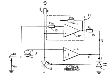
Figure 4 is a schematic circuit diagram of one embodiment of laser driver
circuit according to the invention. A laser diode 1 is again shown, with a back
facet monitor photodiode 2 and its load resistor 3, a voltage reference source 4and integrating transconductance amplifier 5. In this case however the amplifier 5
20 receives (at its inverting input) not only the voltage V~f from the reference source
4 but also the data Vin from a data input 10. Its noninverting input is connected
to receive the feedback voltage at the resistor 3.
Moreover a second, wideband, amplifier 11 is also provided, with an
operational amplifier 12 which is connected to receive the same feedback voltage25 at its noninverting input and the data Vin at its inverting input via an input resistor
13; the voltage gain of this amplifier is determined by this input resistor and a
feedback resistor 14. The amplifier drives a current into the laser diode 1 via a
load resistor 1 5 .
CA 02224727 1997-12-12
PCTJGBg6JO1474
W O 971012~2
In operation, the amplifier 5 drives the diode 1 with a current (in the
direction shown by the arrow in figure 4) of ll . With the notation used previously
this current is given by:
I, = (Yjn + V,.,f--K;SIR + Vs ). G / j~
On the other hand to obtain the voltage V2 output from the wideband
amplifier 11, we sum the currents at the inverEing input, where Rin and Rtb are the
values of the input and feedback resistors 13,14.
Y~n--(~;SIR--Vs ) + Y2--(RSIR--Ys ) o
Rm Rfo
hence Y2 = - R V~" +( R~n)
and, if RL is the value of the load resistor 15,
=--V2 = Rf~ Yjn _ ( l + Rfo ) (RSIR s )
2 RL Rin RL Rin RL
1 5
So that the total laser diode current is
I = I +I = Yin Rfo _ (KSIR--Y5) (l + Rflo) + G (V + V + Y )
Simplifying,
I+K5R( G +1+R,~ Rm) (6
j~) RL
CA 02224727 1997-12-12
W O 97/01202 PCT/GB96/01474
The time varying component of this in terms of the a.c. component Vin~c of the
input signal is
I +KSR( G I R~ ) (7)
j~ RL RLRin
V~ (I + R; GIR~) / ~5R (8
And the corresponding light output is
VinaC(I + R j~ ) / K:~ (9)
R'n ( RL + 1 + GRL ) + 1
We see that if RL/KSR is much less than unity, then this expression is
independent of the laser slope S; moreover if Rin(1 +RL/KSR)/Rfb is much less than
10 unity the light output is solely dependent on fixed parameters of photodiode load
R, and optical feedback transfer function K. In fact a compromise here is
necessary as excessively large values of R can cause a tendency towards
instability. Nevertheless, a worthwhile reduction in slope sensitivity can be
obtained.
The d.c. component of the current I in terms of the d.c. component Vindc
is given by
Yindc + Y"f + yS ~10)
KSR
CA 02224727 1997-12-12
W ~ 97J01~02 PCTJGB96~0147
and the light output
Ldc = 1.~: + V", + Vs ( 1 1 )
which is again slope-independent and moreover maintains the d.c. component of
the input.
In operation, the laser bias point is set by adjustrnent of V.~f. As the circuitis d.c. coupled, the usual bias setting would be just at threshold. This settingwould correspond to Vin = O volts. Any changes in the taser threshold are tracked
by the transconductance amplifier 5. With low-frequency modulation, virtually all
the laser drive is provided by this amplifier; as the frequency increases the
10 contribution from the wideband amplifier 11 becomes more significant and the
proportion of drive current carried by it increases smoothly as the ratio of its gain
(which is substantially constant) to that of the transconductance amplifier (which
is inversely proportional to frequency) increases. Thus the low-speed device
provides the standing laser threshold bias whilst the wideband amplifier
15 contributes just the high-frequency modulation component.
The embodiment of figure 4 is not in a convenient form for
implementation, as the reference voltage is in series with the data signal.
Moreover the photodiode is shunted by the inputs of both amplifiers, which may
cause degradation of performance if the transconductance amplifier 5 has - as is20 typical for low-bandwidth d.c. amplifiers - a low impedance at radio frequencies.
A more practical version is shown in figure 5.
In figure 5, components identical in function to those in figure 4 are given
the same reference numerals. The reference voltage is generated by a
potentiometer 16, and is added to the input voltage Vin by means of an amplifier25 17 with input resistors 18,19 for the reference voltage and Vin respectively, and a
variable feedback resistor 20 for adjusting gain and hence d.c. balance. Owing to
inversion in this amplifier, the reference and input voltages are now applied to the
same polarity input of the amplifier 5 as is the feedback signal from the
CA 02224727 l997-l2-l2
W O 97/01202 PCT/GB96J~1474
photodiode 2, albeit via separate input resistors 21,22. The amplifier 5 has a first
operational amplifier 23, with a feedback resistor 24, feeding via a resistor 25,
value Rint, a second such amplifier 26 which has a feedback capacitor 27 of value
Cin~ to form an integrator. This drives via a resistor 28 an emitter follower pnp
5 transistor 29 which supplies current via a resistor Rout to the laser diode 1.
The construction of the wideband amplifier is unchanged: however note
that the photodiode 2 now operated in photovoltaic mode, and drives the
wideband amplifier 11 directly and the first stage 23 of the integrating amplifier 5
via the resistor 22, avoiding excessive loading of the diode by the input of this
10 stage. A capacitor is also connected from the inverting input of the amplifier 23,
to avoid excessive R.F. currents at the amplifier input.
The wideband amplifier 12 may be a high-performance operational
amplifier such as type HFA1100 manufactured by Harris Corporation or CLC401
from Comlinear Corporation. With the HFA1100 good results were obtained at
15 data rates up to 300 Mbit/s. The others (17,23 and 26) require good d.c. stability
but their frequency response is not critical. The CA3 140 BiMOS op-amp is
suitable .
The cut-off frequency of the amplifier 5 is f=GKRS/2~,
where G = 11 (Cmt Rint RL).
Noting that the amplifier 17 and associated components is outside the
feedback loop, it is necessary to adjust the gain by means of the d.c. balance
control 20 so that the transfer function for the data is equivalent both at high and
at low frequencies. One possible adjustment procedure is as follows:
(a) with a data input of zero volts, set d.c. balance to a nominal starting
value with resistor 20 and set threshold with potentiometer 16 at zero
volts;
CA 02224727 1997-12-12
W O 97~01202 PCTJGB96J01474
(b) observing the laser light output using a d.c. coupled monitor, adjust the
threshold control 16 so that the laser operating point is well into the lasing
region;
(c) apply a 0 to 0.5 volt asymmetrical data signal at 300 Mbit/s to the
data input ~e.g. a single mark followed by 100 spaces), followed by the
inverse sequence and adjust the d.c. balance control 20 until no baseline
shift is seen on the monitor upon repeated switching between the two
signals;
(d) readjust the threshold control 16 until a 0 volt data input signal corrsponds to
10 laser bias just at threshold.
CA 02224727 1997-12-12
W O 97/01202 PCT/GB9~01474
Typical component values for the circuit of figure 5 are as follows:
Reference Vaiue Symbol Value
13 Rin 100 Q
14 Rfb 510 Q
RL 75 Q
16 50 kQ
18 100 kQ
19 10 kQ
50 kQ ~nominal)
21 2 kQ
22 51 Q
24 2 kS2
Rint 10 kQ
27 Cint 1 ~F
28 1 kQ
R~ut 75 Q