Note: Descriptions are shown in the official language in which they were submitted.
' CA 02224783 1997-12-16 ~ ~
Method for writing of data in an optical memory
and apparatus for performing the method
The invention concerns a method for stagewise sequential writing of data in an
s optical memory wherein two or more write units emit light pulses which cause
localized changes in one or more light-sensitive layers in the optical memory, and
wherein the optical memory is transported past the write unit in linear movementalong a path.
10 The invention also concerns an apparatus for stagewise sequential writing of data
in an optical memory and with two or more write units including one or more
pulsating light sources which illllmin~te localized areas in one or more light-
sensitive layers in the optical memory, and wherein the optical memory is
transported past the write units in linear movement along a path.
Optical storage media for digital data in the form of discs or cards combine
substantial storage capacity with portability, i.e. the medium can easily be removed
from the write/read device for storage or for transfer to another write/read device.
~pool tape can also be used for optical data storage and has a number of features in
2 o cornmon with discs and cards, but can in addition store considerably more data
In general the present invention concerns the storage of information on optical
storage media with special emphasis on the possibility of producing a large number
of copies from a master file which contains software, catalogues, music sources,25 video sources and the like.
More particularly, the method according to the present invention concerns the
writing of data in optical media which may be in the form of a tape during a part of
a production process where data are recorded in the medium. With this in mind,
3 o data storage media in the form of cards, e.g., have been m~nl-f~ctured in the form
of a wide, thick tape on a spool and run through a number of processing stages
which correspond to those which are employed on a continuous tape for optical
data storage. After the final stage in the proce-ss, the tape is divided into separate
cards. Even though the tape format entails a restriction which appears to exclude
3s disc media, it is natural to refer to the latter, and this is done to some extent in the
followillg.
In principle all physical formats for a data storage medium can carry memory
AMENDE~ S~
9 CA 02224783 1997-12-16
layers with very different properties. So-called read-only memories (ROM)
represent a subclass of digital optical storage media which have been shown to be
especially well suited to storage and distribution of professional data bases
together with consumer-oriented material such as music, video games, reference
5 works etc. In this subclass data are stored once and for all and can subsequently be
read out repeatedly. A typical example is the compact disc (CD) which is used
arnongst other things for playback of music. A similar, but more fle~ible type of
media is that which is written once and read many times (WORM), where data can
be written on the media by the user. As soon as the data are written in, they cannot
10 be altered, but they can be read a number of times and a written medium of the
WORM type is therefore rather similar to a RO~ Iedia which can be written,
erased and written on again a great number of times are naturally more flexible.
Optical data storage media can offer a substantial storage capacity and also be easy
15 to take out, transport and store for later use. However, with regard to commercial
exploitation, e.g. mass distribution of music recordings, video recordings or similar
types of information, there is also a requirement that there should be the possibility
of transferring large volumes of data from a master source to individual relevant
optical media, for example a disc, tape or card, and in a cost-effective manner.2 o Two fundamentally different methods are known for prerecording data. Firstly,
data can be entered into the medium as an inherent part of the actual manufacturing
process for the medium. Examples of this are punching or injection moulding of
the pit pattern during the m~nllf~cture of so-called CD ROM's, and photographic
exposure and subsequent chemical development of photo-sensitive emulsions, e.g.
25 optical cards which are produced by Dre~ler Technology Co" Palo Alto,
California, USA.
The first method is well-established and has long been commercially exploited.
With regard to the second method, we can refer to the fact that unwritten media
3 o offer the user great fLexibility and elimin~te the need for batchwise production of
different versions of stored material, but represent a formidable challenge for the
data transfer, since large volumes of data have to be written on each initially
unwritten medium at a rate and a cost which ~or important applications must be
able to approach the cheap, high-yield methods which are employed at present in
3 s the manufacture of CD RO~I's. For example, a production line for compact discs
delivers one disc approximately every ten seconds. With a storage capacity on the
disc of, e.g., 600 Mbyte data, this means an average transfer rate of 60 ~Ibyte/s.
This substantially exceeds the write/read rates which can be achieved by to-day's
~.
~E1YoEQ ~T
~ CA 02224783 1997-12-16
, 3 ' .' ,,~, ': '
software, where the maximum read rates for rapidly rotating, parallel track
equipment with a plurality of heads are specified to be around 12 Mbyte/s (LaserFocus World, page 64, August 1993). The write rates are probably much lower
than this.
Data transfer to known optical storage media based on cards, including that offered
by the companies Canon, Drexler Technology Inc. and their licensees, by means ofa laser write beam is several orders of magnitude slower than this. These cards
have capacities which are well under 10 Mbyte, but the slow write rates are still a
10 bottleneck with regard to copying, especially due to the low effective speed which
can be obtained with this forward and backward sc~nning movement of the laser
write beam relative to the card. For example, in GB.-A-2 189 9'~6 (Drexler et al.)
there is disclosed an optical storage mediurn in tape forrn which is attached to a
card base, and which is wound up on a spool and which also has a continuous
5 pattern of parallel, separated and pre-described servo tracks over the entire length
of the tape. The tape can be wound on and off by driven transport spools, while
data are recorded on the tape by a laser-based write/read device. A system wi~h
cards mounted on a drum is known from US patent No. 4 912 312 (Haddock),
where the forward and backward rnovement is avoided. However, placing cards on
2 o a drum and retrieval thereof after the writing appears impractical with regard to
production at high speed and high volume. Haddock also appears to only involve
the use of a single laser write beam.
Further it can be mentioned that optical tape systems for writing and reading
25 between the spools have been developed (C. Terry, "Digital-paper storage: Flexible
optical media boost data density", Electronic Design News, page 77, April 25,
1991). The two systems for writing and reading which have been described do not
appear to be suited to cheap, hi~h-speed recording of data with a view to
distribution of, e.g., music recordings and video recordings. One system involves
3 o the recording of a large number, e.g. 32, of parallel tracks across the width of the
tape. The tape is stationary during this sequence and moves rapidly forward one
step for the ne~t sequence. In a second system a single laser bearn is scanned
across the width of the tape, while the latter moves in such a manner that a
diagonally described track is obtained. Parallel tracks over an area are produced by
3 s a number of passes, which in turn requires the tape to be spooled a number of
tirnes.
For both these systems the data transfer rate is given as 3 Mbyte/s and can be
~.
AMEN0ED St5EET
~ CA 02224783 1997-12-16
- . .
upgraded to 1~ Mbyte/s.
Finally there is from JP patent application JP-A-63096746 lmown an optical
recording system and optical recording medium comprising belt-shaped recording
5 areas extending along the length of the optical recording medium and having a
considerably narrow width. Each of the recording areas is formed with recording
tracks extending transversely over the width direction thereof and thus having aleng~ of a considerably small value. The optical heads record data by modlll~in~a beam of light which scans across the short transversal tracks and in conseguence
10 the range of the deflection angle of the optical beam can be considerably reduced
and this make possible an improvement in the accuracy in condensing the ophcal
beam. Nothing is however said of any improvement in the recording speed and thisoptical recording system does not appear suited to stagewise sequential writing of
e.g. card-shaped optical memories initially assembled as a continuous moving tape
15 or provided on a tape of this kind for high-speed recording of data.
The object of the present invention is therefore to avoid the above-mentioned
drawbacks when transferring data at high speed for copying or production of a
large number of data-carrying media from an individual master medium, while at
2 o the sarne time avoiding the disadvantages of the above-mentioned prior art.
The object is especially to be able to transfer data to storage media which are
physically formatted as cards or tapes. During the writing process the cards should
be joined to form a continuous tape, but could be divided into individual cards
25 after the writing sequence has ceased.
In specific terms' therefore, the object of the present invention is to specify a
method for writing of data at high speed on tape or card-like storage media as well
as to provide an apparatus for performing the method.
The above-mentioned and other objects are achieved according to the invention
with a method which is characterized in providing said two or more write units at a
distance from one another and mutually stepwise displaced in the path's transverse
direction, with the result that a write unit is assigned to a section of the optical
3 5 memory, providing the optical memory with physically separated fields for writing
at each stage, each field substantially corresponding to the section of the optical
memory assigned to a write unit, writing :he data in the transport direction in
separate and successive stages respectively, and writing at each stage a fraction of
.~
A~lEA10'~ F~
~ CA 02224783 1997-12-16
the volume of information which are to be recorded during the writing, said
fraction substantially being proportional to the inverse of the number of write
units; as well as an apparatus which is characterized in comprising two or more
write units provided at a distance from one another and m~ 11y stepwise
s displaced in the path's transverse direction, and that a write unit is assigned to a
sechon of the optical memory, the distance between each write unit being
substantially equal and corresponding to the length of said section of the optical
memory assigned to a write unit, with the result that data are written in the
transport direction in separate and successive stages, each stage contributing al o fraction of the volume of information which are to be recorded during the writing.
The invention will now be described in more detail in connection with embodi-
ments, fun~ment~l principles and the possibilities and capacities which thereby
can be realized, and with reference to the accompanying drawing, in which
fig. la illustrates schematically a device for parallel writing on a tape consisting of
cormected cards and viewed from the side, and
fig. lb is the same viewed from above, and
fig. 2 illustrates how the optical data storage medium is organized with memory
areas on a card and each card cormected to form a continuous tape with sequen-
tially and successively provided write units.
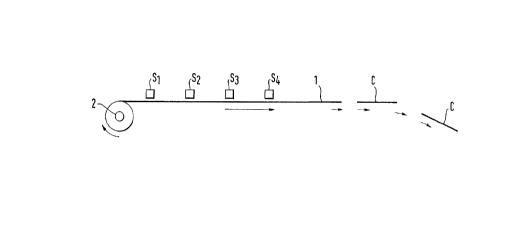
25 Fig. 1 illustrates schem~ically an apparatus for writing of data in an optical
memory and according to the present invention. The actual data storage medium isin the form of a tape 1 which is wound off a storage spool 2 and transported past a
number of regularly spaced write units 5, illustrated here as 4 units Sl,S2,S3,S4- If
the tape 1 is composed of cards C or has to be divided up into cards after the end
3 o of the write sequence, the distance between each write unit S can correspond to the
leng~ of an individual card. After the end of the write sequence the tape is cut up
into cards C, if this is the plefelled, final data storage medium. The use of the tape
format as illustrated in figs. la and lb opens up new possibilities for parallelism in
writing of data by laser. The number of laser units which can wor~ siml-lt~neously
3 s on a single disc or a single card is in fact extremely limited due to the space
requirements. A medium in the form of a tape permits the number of write units to
be increased arbitrarily, provided that the tape is long enough. This is illustrated
more clearly in fig. 2 which shows the tape 1 viewed from above and divided into
~ A~$E.~ 'FrT
~ CA 02224783 1997-12-16
6 .. ':
preferred equally large cards C which when assembled form the tape. The optical
memory area on each card is divided into N fields F, illustrated here as 4 fields Fl,
F2, F3, F~ which extend in the tape's direction of travel. N is also the number of
write units S which are employed along the tape 1 before it is divided into cards. In
fig. ~ N = 4 When the card C enters the first write unit Sl, data are written which
cover a track width corresponding to memory field F~. At the next write unit
memory field F2 is written and so on until all the memory fields Fl, F2, F3, F4 have
been written. If the write speed is R byte/s, the effective write speed for N units
will be NR bytes/s. Given a measured value for NR, the size of N will be the write
l o speed R for every unit S.
An indication will now be given of possible realistic values for the number of
memory fields F on the assumption that the actual systern, i.e. the maxirnum
perrnissible leng,th of the tape 1 which can be written s;ml.lt~neously with N units
1S S is given. Each write unit S occupies a length L, including the required distance
between each wnte unit and the next along the tape's direction of travel, i.e. that
the total write operation occupies a length NL. At present the length L is ass~med
to be between 3 and 20 cm depending on technical factors and costs. Assuming
that the possible length for the data transfer section, i.e. the write area in aproduc~ion line, e.g., is 5 m and L = 15 cm, it is found thatN = 500//15 = 33.
Compared to production lines for other types of cards joined to form tapes, a
length of 5 m for a given write operation is not excessive and the total distance
between the beginnin~ and the end of a multi-operation production line can very
well be 20 m or more. If the tape is composed of cards of, e.g., 10 cm, 200 cards
2 5 will constitute a distance of 20 m between the storage spool and a recording spool
or the cutting point~ The capacity of the storage spool 2 is e~pected to be manythousands of cards.
The wnting process too can be subject to certain restrictions which have conse-
3 o quences for the number N of memory fields F. Each write unit S covers a field F
with limited width on the tape 1. Moreover, when writing by laser, each field F
must be able to be written without overlapping of other fields. The positioning of
each field F with regard to adjacent fields can be~a difficult task and an increase in
the number of fields F in the write units S increases the system's total complexity.
The e~fect on the optimum choice of number of memory fields F caImot be
described in general terms, but must consider explicit tasks concerning each
individual embodiment. Each write unit S includes a detector which guides the
write beam, as is well known in the art. Depending on the medium employed it can
hMENC~D ~HEET
D CA 02224783 1997-12-16
be practical to write each field F in direct con~im~ on of its neighbouring field,
i.e. without any intervening break. Krlown data storage media with predetermineddata positions, e.g. based on the use of spherical microlenses, can, e.g., be
especially relevant in this context. Alternatively the positioning can be made less
5 critical by having a gap between the field boundaries, either physically pre-formed
on the tape 1, or software-controlled as a part of the writing process. If the number
N of fields F is large the number of gaps constitutes a proportionally large area
which cannot be used for storing data. If each gap, for exarnple, is 50 ,um and at
most 3% of the effective memory area width of, for e~ample, 50 mm is lost in thegaps, this means that N = 0.03 50000/50 = 30. If the cards are connected together
to form a tape with the side of the card along the tape's direction of travel, the
effective memory area can, for example, amount to 100 mm, and N = 30 would
then only entail a loss of 1.5% of the effective memory area.
5 The present invention is e~pected to be able to provide write speeds which are at
least as good as or much better than write speeds with the use of known media.
The use of a single laser beam for writing on a rotating disc medium gives up to 1
Mbyte/s in currently available commercial desktop equipment. However, in
production conditions lasers and control systems can be used which can
2 o substantially increase the writing speeds. For e~ample high beam deflection rates
can be achieved acoustically, and there are indications that 3 Mbyte/s can be
achieved with the "Laser-tape" system which employs a single beam. It is indicated
in the literature that addressable laser groups (VCSEL) and positionable lasers
offer the possibility of parallel wnting on a large scale. The same can be achieved
2 5 with spatial light modulators (SLM) combined with a light source. Also known are
directly writable optical memory systems based on electron trap technology, suchas "ETOM" from the Optex Corporation in USA and which is at an advanced stage
of development and is stated to give transfer rates of 15 ~Ibyte/s or more by means
of grey scale coding.
In the present invention, assurning a write rate for each write unit S in the range 1-
10 Mbyte/s, it is possible to achieve a write rate with N units S in the range from N
Mbyte/s - 10 N Mbyte/s. A number of memory fiëlds N of 30 was found to be
compatible with those criteria which were described in the previous paragraph. If a
35 more conservative value is selected, for example N = 10, the write rate when using
the method according to the present invention will be 10-100 Mbyte/s.
It will be possible to combine the optical memory which is employed by the
~NCED S,i~
-
CA 02224783 1997-12-16
': ' . ' , ' ':
; t
method according to the present invention with spherical microlenses which can be
addressed simultaneously by means of a laser cluster. On the basis of prior art the
data transfer rate can be written as:
5 (l) R=nv/8 dbyte/s
where n is the effective number of data point positions under each microlens at the
effective sc~nning rate for the laser system which reads or writes on the medium,
and d is the diameter of the sphere. With d = l0 ~am and n=494 the following is
o obtained:
(2) R = 6 v ~Ibytels, v being expressed in m/s.
The effective scanning rate v should be m~imi7ed irl order to achieve high speed.
15 Two different methods will now be described.
The object of the first is to move the optical write head physically in a forwaFd and
backward movement. This is a slow operation, since commercial optical card
readers normally work at a speed of 0.5-1 rnls. With rnicrolens-based storage
2 o media the laser system will not need to scan at a constant speed.
A second possibility is to move the beam by means of an optical element. This can
achieve a high speed by acoustooptical means, but the strong convergence of the
beam makes this difficult. However, the short length of stroke, for example a few
2 5 mm for high values of N, simplifies the situation and displacement of the beam by
means of movable optical elements can thereby be irnplemented.
A numerical example will illustrate this. Assuming a speed v in the range 0.5-l0/s
gives according to formula (2): R = 3-60 Mbyte/s. This applies to each individual
3 o w~ite unit S. If, for example, l0 write units S are provided, the write rate for the
entire system will be 30-600 Mbyte/s.
In the method according to the present invention an apparatus is employed
according to the invention which also divides the writing process between a
3 5 number of cooperating, but independent write units S based on the assumption that
each individual write unit can write at a speed which is not much less than that of a
single, large write unit. It is well known, however, that there are certain mechanical
restrictions on the maximum achievable scarming rate for a write beam relative to
~..
~MEN0ED Sr:E~T
CA 02224783 l997-l2-l6
~ ~ .
'9 ' ~
the data storage medium. For e~ample the rotation speeds for recent optical discstores have been substantially increased in order to increase the data trarlsfer rates.
In this case mechanical restricting factors will arise in the form of vibrations due to
unevenness in the disc or a decentralized disc mass and acceleration and
5 deceleration effects when files with different radii have to be accessed at high
speed. Systems which write in straight lines are more relevant in this connection,
since a distinction can be made here between scanners which provide a smooth
continuous movement, e.g. based on rotating prisms, or which have no mechanical
movement at all, e.g. acoustooptical deflectors, and those in which a mass is
10 rapidly accelerated or decelerated, e.g. in a forward and backward movement. The
latter case is the most critical, as a number of restricting phenomena will occur,
such as vibrations which reduce the tracking accuracy, power consumption, unit
costs and unit size, etc. Maximum acceleration during the sc~nni~g cycle is a main
parameter, but it can be effectively reduced by employing a plurality of write units
as in the method and the apparatus according to the present invention.
In the case of a harmonic oscillating movement, the effective write speed can beincreased N times by employing N smaller units instead of one large write unit,
thus obtaining a maximum acceleration which is scaled in relation to N. A corre-
2 o sponding increase in speed with a single large unit will lead to a ma~imum acceler-
ation which is scaled by the square of N.
Otherwise it is well known that both acquisition and tracking problems arise at
high speeds. As the speeds increase, increasing demands are also made on a
2 5 number of links in the chain which involve detection, logic and power for control-
ling the beam position. By dividing a write unit S into N smaller units S1, S2,S3,S4
as in the present invention, an increase of a factor of N is obtained in the time
which is available for each individual sub-task, without any reduction in the total
write speed.
When writing in optical storage media there are also physical restrictions with
regard to the size of a so-called b* point in the medium, i.e. an area where a single
bit has to be stored. A certain amount of ener--gy must be supplied to the central
area with an intensity which is above the threshold which is necessary for
3 s registration of the single bit to take place. In practice, however, the light beam is
not stopped at each wnte point in the medium, but the duration of the write pulse is
so short that the scanning movement is virtually effectively "frozen" during thewriting of each bit point. As the bit points become smaller in order to achieve
~.
AMENC'~ S~~ET
~ CA 02224783 1997-12-16
, _ ,
1 0 ' ' ~ t ~ ~
higher storage density and the scann~ng rate is increased in order to give higher
transfer rates, a point is reached where the movement is no longer "frozen" to asufficient extent. With a sc~nning rate of lO m/s the beam moves 107 10-7 ~m =
1 ~n in the course of lOO ns, which is far above what is permissible for a high-
5 density storage medium. It should be noted, however, that optical data storagemedia based on spherical microlenses are less vulnerable in this respect. A
reduction in the pulse duration will avert the problem, but another problem may
arise, viz. that it will be difficult to supply sufficient energy in the time which is
available. This in turn leads to higher laser output and higher costs. Independently
10 of this, simultaneous reading and writing in order to control the actual writing
process, e.g. and to achieve a greater degree of reliability or control of grey scale
coding, will become more diflicult and more expensive as the time which is
available for writing in each bit point position is reduced. By employing a method
according to the invention where the writing of the data is performed separately15 and in successive stages by means of two or more write units and by means of an
apparatus which performs such a method, the combination of high write speed,
adequate process quality and small diameter, i.e. high energy in the write point, in
other words high storage density and high data transfer rates, can still be achieved
without the problems which are present in the current prior art.
~ENC.'C ~.'FFr