Note: Descriptions are shown in the official language in which they were submitted.
CA 0222492~ 1997-12-1~
SVG-4022
MOVING INTERFEROMETER WAFER STAGE
FIELD OF THE lNV~NlION
This invention relates generally to photolithography as used
in semiconductor manufacturing, and particularly to a wafer stage
with accurate positioning and alignment.
BACKGROUND OF THE lNV~NllON
In the manufacture of semiconductor devices and flat panel
displays, photolithography or microlithography is often used. A
substrate or wafer stage on which a semiconductor wafer or other
substrate is placed is used to align and position the wafer
during exposure. A wafer stage used in aligning and positioning
a wafer is disclosed in U.S. Patent No. 4,952,858 entitled
"Microlithographic Apparatus" issuing August 28, 1990 to Daniel
N. Galburt, which is herein incorporated by reference. Therein
disclosed is an electromagnetic alignment apparatus including a
monolithic stage, a substage, and an isolated reference
structure. Another wafer stage is disclosed in U.S. Patent No.
5,285,142 entitled "Wafer Stage With Reference Surface" issuing
February 8, 1994 to Daniel N. Galburt and Jeffrey O'Connor, which
CA 0222492~ 1997-12-1~
SVG-4022
is herein incorporated by reference. Therein disclosed is an
electromagnetic substage and an electromagnetic monolithic stage
coupled such that one follows the other and having a single
reference surface extending over the entire range of motion of
the monolithic stage. Additionally disclosed therein are
interferometer return mirrors placed on the wafer stage.
Interferometer return mirrors are used in an interferometer
alignment system for accurately positioning and aligning a wafer
stage. The interferometer return mirrors have always been placed
on the wafer stage with the interferometers placed off of the
wafer stage. While this has been acceptable for most
photolithographic operations, as the wafer size becomes larger
and the feature size of the circuit elements become smaller,
there is a need to improve the structure of wafer stages to
improve positioning and alignment of the wafer. The return
mirrors in an interferometer system must be stable, and are
therefor usually large and heavy. Because of the increasing
wafer size, the wafer stage must travel longer distances. This
results in large, heavy interferometer return mirrors being
placed on the wafer stage. As a result, it is often difficult to
quickly and accurately move the wafer stage. Additionally, the
CA 0222492~ 1997-12-1~
SVG-4022
mirrors being mounted on the wafer stage are sensitive to
rotation of the wafer stage which results in errors being
introduced, often referred to as cosine errors. Additionally,
when the wafer stage is rotated, an optical signal loss occurs
which limits stage travel and rotation and requires a larger,
more powerful laser illumination source to be used with the
interferometer. Accordingly, there is a need to improve upon the
conventional wafer stage structure to enhance positioning and
alignment accuracies as well as reducing the weight and power
required in conventional wafer stages.
SUMMARY OF THE lNv~NLlON
The present invention is directed to a wafer stage having a
plurality of interferometers placed thereon. The interferometers
move with the wafer stage. Two stationary orthogonal return
interferometer mirrors are placed adjacent the wafer stage and
are used in conjunction with the interferometers placed on the
wafer stage in order to obtain accurate alignment and positioning
information. In one embodiment, the wafer stage is mounted
vertically and a laser beam is folded using a penta prism and
directed to the plurality of interferometers on the wafer stage
CA 0222492~ 1997-12-1~
SVG-4022
through a plurality of beamsplitters and fold mirrors.
Accordingly, it is an object of the present invention to
reduce errors in positioning and alignment of a wafer stage.
It is a further object of the present invention to reduce
the size and weight of a wafer stage or to increase the travel
distance of a wafer stage without increasing the size or weight
of the wafer stage.
It is an advantage of the present invention that a lower
power laser illumination source may be used.
It is a further advantage of the present invention that it
is more tolerant of rotation or twisting of the wafer stage.
It is a feature of the present invention that
interferometers are placed on the moving wafer stage.
It is a feature of the present invention that the stationary
interferometer return mirrors are placed off of the moving wafer
stage.
It is a further feature of the present invention that an
appropriate system of mirrors such as a penta prism is used to
maintain a beam orthogonal to the stationary return mirrors
irrespective of some twisting or rotation in the substrate plane
of the wafer stage.
CA 0222492~ 1997-12-1~
SVG-4022
These and other objects, advantages, and features will
become readily apparent in view of the following more detailed
description.
BRIEF DESCRIPTION OF THE DRAWINGS
Fig. 1 schematically illustrates the present invention.
Fig. 2 is a perspective view illustrating one embodiment of
the present invention.
DETAILED DESCRIPTION OF THE PREFERRED EMBODIMENTS
Fig. 1 schematically illustrates the present invention. A
wafer stage 10 has a wafer 12 placed thereon. The wafer stage 10
has a right-handed, (X, Y, Z) Cartesian coordinate system 11
centered over the wafer 12. Also placed on the wafer stage 10
are four laser gauge type interferometers 14 and 16 posltioned
along the X-axis and the Y-axis respectively, of the edges of the
wafer stage 10. Light from the interferometers 14 and 16 travels
to two orthogonal reference mirrors 30 and 32. Light from
interferometers 14 travels in the Y-direction to the stationary
return mirror 30 located with its face parallel to the X-Z-plane.
Light from interferometers 16 travels in the X-direction to a
CA 0222492~ 1997-12-1~
SVG-4022
second stationary return mirror 32 located with its face parallel
to the Y-Z-plane. The term light as used in this application is
meant to refer to electromagnetic radiation of any wavelength,
and not only to light in the visible spectrum.
In the simplest configuration three single-axis plane mirror
type interferometers, incorporating corner cubes occupy any three
of the four interferometer positions. When illuminated each
plane mirror interferometer has a metrology axis in the direction
of the illumination that should be set normal to the associated-
reference mirror. As shown in Fig. 1, it may be desirable to add
a fourth interferometer of the same type to provide nominally
redundant information for error correction and other purposes.
In this configuration, the four interferometer laser beams are
aligned in a plane that is nominally parallel to the wafer plane.
A11 alignment information furnished by the laser gauges or
interferometers 14, 16 is referenced to a plane parallel to the
wafer plane. For the critical overlay alignment requirements of
microlithography, it is necessary to provide small motion control
and alignment of the wafer in six degrees-of-freedom, three in
the wafer plane and three perpendicular to the wafer plane. The
wafer stage 10 is free to move relatively large distances, more
CA 0222492~ 1997-12-1~
SVG-4022
than one wafer diameter, in the in-plane or X-Y-directions, as
long as the interferometer laser beams fall onto the reference
mirrors 30 and 32, and rotation about the Z-axis is typically
restricted to less than about several milliradians. For the
other three degrees-of-freedom, system constraints allow only
very small motions.
The preceding configuration provides information needed to
control the three in-plane degrees-of-freedom. Alternative
means, not necessarily optically-based, must be established to
provide control information for the other three. The faces of
the two reference mirrors 30 and 32 define five degrees-of-
freedom. Five plane mirror type interferometers can be located
on the wafer stage 10 and directed at the reference mirrors 30
and 32 to provide useful information for these five degrees-of-
freedom. In one convenient configuration, the five
interferometers may include the two interferometers 16 and one of
the interferometers 14, for example the rightmost one, with the
addition of two more interferometers, not shown. The two
additional interferometers may be placed, one under the selected
rightmost interferometer 14, and the other located under either
one of the interferometers 16. The two additonal
CA 0222492~ 1997-12-1~
SVG-4022
interferometers, not shown, therefore are offset in the negative
Z-direction, into the page, with respect to the interferometers
14 and 16. Mirrors 30 and 32 would be made wider in the same
negative Z-direction to accommodate the additional interferometer
laser beams. Typically, the measurement axis of three
interferometers would lie in a plane parallel to the wafer. The
measurement axis of the other two interferometers would lie in a
parallel plane offset along the Z-axis. The remaining required
sixth degree-of-freedom, Z-axis location, requires an additional
reference structure. Two forms of such a reference structure of
particular interest are both structures parallel to the wafer
plane. One structure, not shown, located above the wafer 12
surface could hold one or three sensors that measure the distance
to the wafer thereby providing Z or all three out-of-plane
information. Alternatively, the structure could be a mirror with
its face parallel to the X-Y-plane. The reference structure
mirror provides a flat reference surface parallel to the plane
defined by the wafer 10. The Z or all out-of-plane metrology
information could be measured with one or three sensors,
including interferometers, on the wafer stage.
All of the reference items must be mechanically stable with
CA 0222492~ 1997-12-1~
SVG-4022
respect to each other and the photolithography image that will be
printed.
The interferometer metrology axes should be spaced as far
apart as possible - typically of the order of one wafer diameter.
It is possible to replace several single-axis interferometers
with appropriately selected multi-axis interferometers.
The Hewlett-Packard Company, Test and Measurement
Organization, manufactures an extensive line of laser gauge
components that are useful with this invention. These components
belong to their commercial product line listed as "laser
interferometer positioning systems" in their current 1996
catalogue. Catalogue components relevant to this invention
include: laser heads; beam directing optics; one-, two-, and
three-axis interferometers; fiber optic-fed detectors; and the
associated metrology electronics.
Each interferometer 14 and 16 has an output 18. The output
18 is coupled to a photodetector, not shown, through fiber optic
cable 20. The fiber optic cable 20 may be mechanically coupled
to the interferometer or it may be mechanically decoupled and
only coupled optically in a manner similar to the optical input
feed options described below.
CA 0222492~ 1997-12-1~
SVG-4022
Each of the interferometers 14, 16 should be illuminated so
that the metrology axis is maintained as perpendicular to the
associated-mirror 30, 32 face as possible. The interferometers
14, 16 can be illuminated as a group with the illumination
distributed from a less precisely positioned single-axis stage to
optics on the wafer stage 10, for example as illustrated in Fig.
1. Alternatively, the illumination can feed each of the
interferometers 14, 16 separately with the distribution optics
not on the wafer stage 10, but on a less precisely positioned
stage. This latter concept is illustrated in Fig. 2.
A first penta prism beamsplitter 22 is placed adjacent one
of the interferometer laser gauges 16. A second penta prism
beamsplitter 24 is placed adjacent the other interferometer laser
gauge 16. A beamsplitter 26 is placed adjacent penta prism
beamsplitter 24 and is used to fold or direct light to a second
beam folder or fold mirror 28 adjacent one of the interferometer
laser gauges 14. A laser 34 is positioned off of the wafer stage
10 and directs a beam of light 37 parallel to the X axis. A
penta prism 36 is positioned to receive the light from laser 34
and directs the light to penta prism beamsplitter 22 on the wafer
stage 10. A beamsplitter 38 directs a portion of the light from
CA 0222492~ 1997- 12- 1~
SVG-4022
the laser 34 to a wavelength monitor 40.
The penta prism 36 iS mounted so as to follow, in the X
direction, the travel of the wafer stage 10, as indicated by the
double headed arrow 35. Current technology laser gauge lasers
are relatively large and typically would be mounted on a
stationary platform so that it is convenient to illuminate the
interferometers as shown in Fig. 1 and Fig. 2 starting with
penta-prism 36 moving on a single-axis stage that moves in the
direction of arrow 35 parallel to the laser light and normal to
reference mirror 32. Although the interferometer metrology axis
orthogonality to the reference mirror is sensitive to rotations
in the wafer plane by the single-axis stage, penta-prism 36 can
be replaced by a fold mirror if these rotations are small enough.
In principle, the laser 34 could be attached directly to the
one-axis stage and aligned with its light perpendicular to mirror
30. The wavelength monitor 40 iS used to monitor and determine
the status of the atmosphere as it affects the laser 34.
In operation, the laser 34 emits a light beam 37, a portion
of which is split by beamsplitter 38 and directed to the
wavelength monitor 40. Most of the light beam 37 iS directed to
the penta prism 36, which redirects the light to penta prism
CA 0222492~ l997- l2- l~
SVG-4022
beamsplitter 22. The penta prism beamsplitter 22 permits a
portion of the light to continue to penta prism beamsplitter 24.
A portion of the light is reflected by penta prism beamsplitter
22 and directed to the adjacent interferometer 16. One of the
emerging beams is directed to the adjacent interferometer laser
gauge 16 and is perpendicular to the beam of light entering the
penta prism beamsplitter 22. The light enters the interferometer
laser gauge 16 and is directed to and reflected from the return
mirror 32. The output 18 iS carried to a photodetector, not
shown, by fiber optic cable 20. From this output, information is
obtained as to the location of the wafer stage 10, from which
position and alignment information is calculated using
conventional known techniques. The light entering penta prism
beamsplitter 24 iS similarly directed to the adjacent
interferometer laser gauge 16. A portion of the light is split
and directed to beamsplitter 26. A portion of the light entering
beamsplitter 26 iS directed to the adjacent interferometer laser
gauge 14, and a portion of the light is folded to beam folder or
fold mirror 28. The fold mirror 28 folds the light and directs
it to the adjacent interferometer laser gauge 14. While four
interferometer laser gauges 14 and 16 are illustrated, it should
12
CA 0222492~ l997- l2- l~
SVG-4022
be appreciated that only three are generally needed. However,
four may be used for redundancy if desired.
Typically, the laser 34 may be placed a distance 50 to 150
cm from the penta prism 36. In some applications, where the size
or heat of the laser is undesirable, the laser 34 may be placed
even further away. The penta prism 36 may be mounted from 20 to
50 cm from the furthest extended travel of the wafer stage 10.
The two interferometer laser gauges 14 may be separated by a
distance of approximately 20 cm. Similarly, the two
interferometer laser gauges 14 may be separated by a distance of
approximately 20 cm. Each interferometer 14 and 16 iS typically
placed 2 to 32 cm from the return mirrors 30 and 32,
respectively. The above dimensions are only given by way of
example, and other dimensions may be appropriate depending on the
particular application.
Many advantages are obtained by the structure of the present
invention. By placing the mirrors off the wafer stage, the
mirrors can be made larger and more stable, and more accurately
manufactured at lower cost. Additionally, the wafer stage can be
made smaller and of less weight. Wafer stage rotation accuracy
is also improved by increasing the separation of the paired
CA 0222492~ 1997-12-1~
SVG-4022
interferometers without increasing the size of the wafer stage,
which would normally be required if the mirrors were mounted on
the laser stage as is conventionally done. Additionally, it is
also possible to mount the interferometers so as to place them in
or close to the wafer plane, eliminating errors such as Abbe
offset error. Additionally, with the structure of the present
invention, the angle at which the input beam enters the
interferometer does not influence alignment. Therefore, some
degree of rotation about the Z axis, of approximately two
milliradians, is possible without affecting alignment or position
accuracy, depending upon the type of interferometer laser gauge
used. Typically, the wafer stage 10 has three laser gauge
interferometers placed close to the wafer plane for measuring
three degrees of freedom, X-translation, Y-translation, and Z
rotation. The three laser gauge interferometers are preferably
mounted on the wafer stage 10 forming a right triangle, with the
two short legs between the 90~ angle being parallel to the
respective longitudinal axis of the return mirrors 30 and 32.
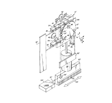
Fig. 2 is a perspective view generally illustrating an
embodiment implementing the schematic drawing of Fig. 1. A wafer
stage 10' has a wafer chuck 12' placed thereon. A wafer, not
14
CA 0222492~ 1997-12-1~
SVG-4022
shown, is placed on the wafer chuck 12'. An interferometer 14'
is positioned at one corner of the wafer stage 10'. A pair of
interferometer laser gauges 16' are positioned parallel to the Y
axis. Accordingly, in this embodiment only three interferometer
laser gauges 14' and 16' are needed in order to obtain sufficient
positioning and alignment information. The wafer stage 10'
typically has three degrees of freedom in the Y-translation, X-
translation, and Z-rotation. Between the pair of interferometers
16' are placed the first beamsplitter 22', which may be a penta
prism, and a second beamsplitter 24', which also may be a penta
prism. A pair of beam folders or fold mirrors 44 and 52 are used
to direct the light beam to one of the interferometers 16'. A
beam folder or fold mirror 46 is associated with the other
interferometer 16' and directs the light beam thereto. Beam
folder or fold mirror 48 and fold mirror 50 are associated with
interferometer 14' and directs the light beam thereto.
Associated with each interferometer 14' and 16' is an arm 54
having a reference mirror 56 thereon. The wafer stage 10' rides
on air bearings 42, preferably three are used in a triangular
arrangement, with only two being illustrated. The air bearings
42 ride on a plane surface, not shown. When the wafer stage 10'
CA 0222492~ l997- l2- l~
SVG-4022
is positioned vertically, a counter force cylinder 58 is used to
compensate for the weight of the wafer stage 10'. The counter
force cylinder 58 is attached to a support 60 which is coupled to
a motor or linear drive 62. The motor or linear drive 62 permits
the wafer stage 10' to be moved in the X direction, indicated by
arrow 64. A stationary return mirror 32 ' iS placed parallel to
the Y axis formed by the pair of interferometer 16 ' . The return
mirror 32 ' has a length sufficient to accommodate the entire
travel distance of the wafer stage 10' in the Y direction. A
stationary return mirror 30 ' iS positioned parallel to the X
axis, and has a length sufficient to accommodate the entire
travel distance of the wafer stage 10' in the X direction.
Accordingly, the stationary return mirrors 30 ' and 32 ' can be
made relatively large and stable because they are not placed on
the wafer stage 10'. Also associated with the wafer stage 10' is
a calibration detector 66. Calibration detector 66 iS used in
some alignment and positioning operations.
In operation, a laser source 34 ' provides a beam of light
37 ' which is directed parallel to the X axis. The beam enters a
penta prism 36 ' which folds or redirects the beam 90~ to a
beamsplitter 22 ', which may be a penta prism. The beamsplitter
16
CA 0222492~ l997- l2- l~
SVG-4022
22 ' directs a portion of the beam to a fold mirror 46 and another
portion of the beam to another beamsplitter 24 ', which may be a
penta prism. The fold mirror 46 directs the beam to a first
interferometer 16'. Beamsplitter 24 ' directs a portion of the
beam to another fold mirror or beam folder 48 and a portion of
the beam to a fold mirror or beam folder 44. The fold mirror or
beam folder 48 directs the beam to a fold mirror or beam folder
50, which directs the beam to interferometer 14 ' . The beam
received by the beam folder or fold mirror 44 directs the beam to
beam folder or fold mirror 52. Beam folder or fold mirror 52
then directs the beam of light to the second interferometer laser
gauge 16'. The three interferometer laser gauges 16' and 14 ' are
used in association with the stationary mirrors 30 ' and 32 ' to
accurately obtain position and alignment information on the
precise location of the wafer stage 10' in X-translation, Y-
translation and Z-rotation. The three interferometers 14 ' and
16' preferably form a right triangle in a plane parallel to the
planar surface of the wafer chuck 12 ' . Preferably, the
interferometer laser gauges 14 ' and 16' are placed near the wafer
plane, thereby eliminating errors such as abbe offset errors.
Additionally, the structure of the present invention with the use
CA 0222492~ 1997-12-1~
SVG-4022
of penta prisms helps to maintain the alignment of the
interferometer laser gauges irrespective of small rotations or
twisting about the Z axis, and therefore, is less sensitive to
rotation than conventional alignment systems using
interferometers.
The present invention improves the range of travel of a
wafer stage having less mass or weight, while at the same time
improving alignment and positioning accuracies and being less
sensitive to certain errors introduced by rotation, or having the
interferometers positioned away from the wafer plane.
Accordingly, the present invention improves and advances the art.
Although the preferred embodiment has been illustrated, it
will be obvious to those skilled in the art that various
modifications may be made without departing from the spirit and
scope of this invention.
18