Note: Descriptions are shown in the official language in which they were submitted.
CA 02224979 1997-12-15
WO 97f(30565 PCT/US96/I0414
CDMA C~MMUNICATION SYSTEM IN ~IICH BIT RATES
ARE DYNAMICALLY ALLOCATED
$ACICGROUND OF THE INVENTION~
This invention relates to communication systems;
and more particularly, it relates to multipoint-to-point
CDMA communication systems.
As used herein, the term ~~multipoint-to-point°~
refers to a communication system in which multiple
transmitting stations, which are located at respective
points, simultaneously send separate data blocks to a
single receiving station which is located at one other
1o point. That is, a first data block is sent by a first
transmitting station, a second data block is sent by a
second transmitting station, etc.; and, any number of these
data blocks can be sent at the sx~me time.
One way to operate such a system is to have each
transmitting station send its data as an amplitude
modulated, signal in its own wireless channel which differs
in frequency for each transmitting station. However, if
_ the total number of transmitting stations in the
communication system is large, then a corresponding large
number of separate frequency bands is required.
Alternatively, each transmitting station can send its data
CA 02224979 1997-12-15
WO 97/00565 PCT/US96/10414
-2-
over a separate optical fiber to the receiving station.
However, when the receiving station is remotely located
from the transmitting stations, too much connecting optical
fiber is required.
By comparison, with a multipoint-to-point CDMA
communication system, all of the transmitting stations send
their data in either a single wireless channel or a single
optical fiber. By the term °°CDMA°° is herein
meant °°Code
Division Multiple Access.°° In a CDMA system, each
1o transmitting station encodes the data that it sends v~ith a
respective spreading code which is unique to that station.
Then, the encoded data from all the transmitting stations
is sent simultaneously on a single Wireless channel/optical
fiber in one frequency band to the receiving station.
In the receiving station, the data from any one
particular transmitting station is recovered by exclusive-
oring the composite CDMA signal with the same spreading
code which was used to encode the data. One prior art CDMA
receiving station is described in U.B. Patent 4,908,836 by
Rushforth, et al., entitled °°Method and Apparatus for
Decoding Multiple Bit Sequences That ~rre Transmitted
simultaneously in a single Channel°~. Also, another CDMA
receiving station is described in U.B. Patent 5,031,173 by
Short, et al., entitled °°Decoder for Added Asynchronous
Bit
Sequences°°. Both of these patents are assigned to the
assignee of the present invention.
In the prior art, each transmitting station can
have a first-in-first-out data buffer (FIFO data buffer)
which temporarily holds the data that is to be transmitted.
pith a FIFO data buffer, the data that is to be transmitted
is written into the buffer from an external source at one
bit rate, while simultaneously, data is read from the
buffer and transmitted to the receiving station at a
different bit rate. Consequently, if the rate at Which
data is written into the buffer exceeds the rate at which
data is read from the buffer during a long time period,
CA 02224979 2006-02-02
_~~
then z~n oz~erload GGZ2.C~1.'t10?1 C2iT1 occuz whewe_i.n the storage
capacity of the data 2~utfex i9 oa~c~r~d~d.
~:lsr~, . in the ~pritir a~'t, tie nnmbor ~nf gt~,t~,cns
which actu~~.ly transmit cDM~ data at any one time instant
carp wary. gzoatly. For e~s~.mple, suppc~sa that ti-m CD.M~,
comm~unicat.ic~n system includos loo c~iffaront tran9mitting
stgtiflns _ ~n thgt cress, the number of tr~xnsm3ttxrsq
statzDns which act-unlly trx~nr~it CDN.A data ~.t the ssm~ time
instant osn vt~r~ 'rom 1 to 1c~0. 'thus, whoa each
transmitting statifln sends its data at a fig.~d bit rate
then a dilemma ooc~xrs. if the bit rite of each
transmitting station is set high, the total bit rate
capecitg of the CD2~ natwor~ can be esoeadad whenever a -
large number ad st~tion.s ars actually traasmitti ng.. But if
the bit rate of each transmittiTag staffoa is set lace, then
a bLffr~r o~rez3oa~3 can fy$duently .occur.
Also, the prior art includes the follow~.ng
publications "Design ' Study for - a CDMA Based Third
Generation Mobile R.a~io System" by Baler, et al.., IEEE
Journal on Selected Areas in Communication Vol.. 12,
No.. -4 , l May 1994, lvtew York, tTSA, pages 73 3 - 7~3
(hereinafter reference Dl) ;. "The . Grade of Service for ,
Integrated Voice/Data Wireless DS-CDM~. Networxs~' by
Guo, et al.. ; Vol. 2, 1 'May 1994, ~Ixast~.~tute of
Electrical and Electronics- Engineers, pages 1104-1110
(hereinafter ref erence D2 ) ; and ' U _ S . ~~ Patent 5,12 8 ,'9 59
(hereinafter reference D3) . Refezence 'D~, discloses a
communication system a~n ~ohich data is transmitted at
multiple bit 'rates on a single CDMA .channel; however.,
reference D1 does not disclose any feedback circuit or
feedback method whereby each transmitter can periodically
request different'bit rates at spaced-apart times, and
periodically be granted different bit rates .based on
those .requests and available channel capacity. Further,
reference D1 does not d~.sclose any circuit which tallies
alb.. of the bit rates which ~ are granted to the, individual
tx-an9mitting stations and maintains the tally below a
CA 02224979 2006-02-02
- 3A -
predeterxr:~.uec3 x~axim~,sm aggrEgate bit rote. Reference L.'r.
disci ores a communication s~~stem in which a decision to
allow a station to have access to a Chi channel i.s md.de
ba9ed on the total m.imber of other stations t:7at
presently ~iave nu~:horz~ation to transmit, hut
reference D2 cannot sense az~y ~~anginc~ bit rata
transmission re~n~irements which each station may have;
and thus after a decision is made to let a station use a
CDi~A C lanrlel, the perlnitt'd translrrission rate for that
station is not -clanged. neie~ence D3 describes a
Communication system in wh-~~ch several base stations
transmit in d.iiyerent bandxidths with diiferEnt
enCZ~rption keys. ~iowever, reference D3 does n.ot disclose
Gny circuit or method of 'trans~ntting at- dirTPr~nt bit
xates in an~J one bandwidth.
Accord~.t~gZy; a ~ prfmary object of the present
invention is to provide an improved ~ultipair~t-to-point
communication system in ~nicli the above drawbacks erg
overcome.
H~I~RY o~ T$E Ion:
'at~.th the present invention, a CDR communicstion
system is provided fn ~rhich bit rata .are dynamically
allocated. This CnMA communication system includes a
plurality of CDMA transmitting stations and a single C
recs~:ving station, all of xh~.ch are intercougled~ to ee.cb
other over a CDMA channel sad a feedbaclt channel. Each
CDMA transmitting station includes a control circuit which
sends cantr4l signals on th4 CDM.A channel in spaced apart
time intervals ~h3c~h request respective lit rates on the
cpMA channel ; and, the CDl~tA receiviflg tstt~tioa includes a
hit rate a:7.locatiag circuit ~rhich receivers a,nd responds to
the contrbl signals by sending feedbe~c~C messages over the
feedbxeek ch~nn81 that nddrersa in~ividtaa~~. CDKA transmitting
s,tat3oag and grant respective hit rates to th.e nddrsssed
CA 02224979 2006-02-02
- 4 --
station. Each CD~1A transxnitl:~.ng station receives those
feedback messages which have its address, acrd each CDZ~A
transmitting station sends CDbIA. data on the CD~MA chanmel
at th,e bit rates granted S.n the received Feedback
messages.
Tz~ each transau.tting statipn, a data b~u~fer
stores a time vax~~.ng number of data bytes that axe to be
sent, end each transmitting statioa requests respective
bit rates on the CDMA channel by sending Control signals
which xe8resent that number. Ia the receiving station,
the bit rate allocating. circuit ta~.~.ies the bit rates
which xt grants in the feedback messages, aza,d it maintains
that tally below a predetermined maxi~aum aggregate bit
rata for the Q~MA charcoal.
BRIEF T~ESCRIPTION OF THE DRAWINGS:
F3g. 1 shows an overview of a CDMA communication
system which constitutes aae preferret~ embodiment of the
present invention.
Fig. 2A shaves a format far CDMA signals which
are sent by several CDMA tzansmittirig stations in the Fig.
1, comrcmmication syst~.
Fig. 2r3 shaves a ~oriaat for f6adback messages
mhi.ch are sent by one CDMA receiving station to several
CDMA tz~ansmitting stations in the Fig. 1 c~nunication
system.
Fig. ~ is a detailed Circv,~.t diagram. of a
preferred ambodimeilt for each CI»!A transmit~Ca.ng stati.ok~ in
Fig. 1.
Fig, 4 is a detailed circuit diagram of a
preferred embodixuetrt for the CnMl~ reCaxvrng station in
Fig. 1.
CA 02224979 1997-12-15
WO 9'7/00565 PCT/US96/10414
-5-
Fig. 5 shows a preferred embodiment of a bit rate
allocation program which is executed by the CDMA receiving
station,in Fig. 4.
Fig. 6 is a timing diagram which ill.atrates a
s sequence by which the CDMA transmitting stations and CDMA
' receiving station in l~ig. 1 change the bit rate at which
they respectively transmit and receive data.
DE'~'A'~3.FD DESCRIPT ON~
Referring now to Fig. 1, a CDMA communication
to system which constitutes one preferred embodiment of the
present invention will be described. This Fig. 1
embodiment includes a plurality of CDMA transmitting
stations Tsi, Ts2, T83, . . . etc.; and it includes a single
CDI~A receiving station Rs. All of the CDMA transmitting
15 stations and the single CDMi~ receiving station are
interconnected to each other by a single coaxial cable 10
as shown.
suitably, the coaxial cable 10 is a pre-existing
cable in a conventional cable television network. In that
20 case, the cable 10 carries standard cable television
signals which in Fig. 1 are labeled TV; the CDMh
transmitting stations are located in respective houses
which receive the TV signals; and the CDMA receiving
station is located in the cable television plant which
25 supplies the TV signals. All of the TV signals occur in a
frequency band FBo, and they are not used by the CDMA
transmitting stations or the CD1~A receiving station.
Each CDMA transmitting station Ts~ operates by
sending signals CDMA~ over the cable 10 to the receiving
30 station R8. That is, station T81 sends signals CDMA1;
station Ts2 sends signals CDMh2; etc. Any number of these
signals can occur on the cable 10 simultaneously whereupon
they axe added together to form a composite signal CDMA.
Each of the signals CDMAl, CDMA~, etc., fully occupy the
CA 02224979 1997-12-15
WO 97/00565 PCT/US96/10414
-6-
same frequency band FB1 which is separate from the frequency
band FBA.
In response to each of the CDMA~ signals, the
receiving station Rs sends a feedback message M~ on the
cable l0 back to the corresponding transmitting station TBi.
These feedback messages occur in a frequency band FB2 phich
is separate from the frequency bands FBo and FB1. since the
three frequency bands FBo, FBl, and FB2 are all separate
from each other, the corresponding TV signals and CDMA
signals and feedback messages M~ can all occur on the cable
to at the same time without interfering with each other.
Fig. 2A shows a preferred format for each of the
signals CDMFr~; and Fig. 2B shows a preferred format for each
of the feedback messages M~. In Fig. 2A, each of the CDMAI
signals includes a header 20 that is followed by a block of
data 21, which is a fixed number of data bits. This header
identifies a destination 20a to which the data 21 is
forwarded over a network 11 by the receiving station R8.
Network 11 can be any conventional communication network,
20 such as a telephone network.
Also, the header 20 includes a count 20b; and
this count constitutes a request by the transmitting
station T8~ to send its data 21 at a certain bit rate.
Specifically, when the count is high, the count constitutes
a request to transmit data at a correspondingly high bit
rate; whereas when the count is low, the count constitutes
a request to transmit data at a correspondingly low bit
rate. Preferably, each transmitting station Ts~ includes a
first-in-first-out data buffer which stores a time varying
number of data bytes that are to be sent. In that case,
the count 20b which is sent in the header equals the number
of data bytes that are stored in the data buffer.
within the receiving station R8, the count 20b in
each of the CDMA~ signals is received. Then, in response to
the count CNT~, the receiving station RS sends the feedback
messages M~ over the cable 10 which address the CDMA
CA 02224979 1997-12-15
WO 97/00565 PCT/US96/I04I4
transmitting station T8~ and grants a particular bit rate
to
the addressed station. This is shown in Fig. 2H wherein
each message Mi includes a hemder 25; and that header may,
or may not, be followed by a block of data 26. In the
header 25, an address AF is included which addre
sses a
particular CDMA transmitting station TBI. Also in the
header 25, a bit rate DRS is included which is granted to
the addressed transmitting station.
In one preferred embodiment of the CDrt~r receiving
l0 station which will be described shortly in conjunction with
Fig. 4, a microprocessor is included which tallies the bit
rates that are granted in the feedback messages Mi. By
keeping this tally, the cDMA receiving station R8 is able
to grant bit rates in 'the messages Mi which maintain the
total bit rate for all of the CDMAj signals below a
predetermined maximum aggregate bit rate BRm~.
For example, suppose the maximum aggregate bit
rate for all of the CDMA~ signals on the cable 10 is ten
Mbps
(10 megabits per second); and suppose further that only
three stations TBi, Ts2, and Ts3 have data to transmit. In
that case, at one time instant, the respective bit rates
which axe granted to the transmitting stations T81, Ts2 and
Ts3 could be 1 Mbps, 2 Mbps and 6 Mbps. Thereafter, due to
a change in the count signals CNTi, the respective bit rates
which are granted could be 5 Mbps, 1 Mbps, and 4 Mbps.
suitably, the maximum aggregate bit rate BRma~ is
set at about 9o percent of a bit rate at which errors start
to occur in the data that is recovered by the receiving
station Rs. This leaves about 10 percent of the aggregate
bit rate for any stations Ts~ which are not currently
transmitting CDMA~ signals to start their transmissions.
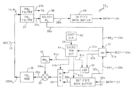
Turning now to Fig. 3, a preferred internal
- structure for each of the CDMA transmitting stations T8~
will be described. This Fig. 3 embodiment includes several
CA 02224979 2006-02-02
~.g_
el6C't:rDIllC lriCJdlllf39 9D~4~.; Gild e~lC~1 Ot th696 IriDt~lul~8 Z.9
identified below in Table 1.
T~z~ i
~t~ D$8C$I~TIQp
,5 3 o . , , , , , A f first-in-first-out Bata huff er (F2F0?
whioh reaeivee datn an an ~.nput 3 Oa and
sends c9nta an an output Sob. This -data
buffer generates the co~xnt signal C~TTi,
on an output 30c, equal to the number
of data bptes that are stored in the
data buff er.
33~....... A microprocessor, such ate a Motorola
6800 r~hip, including an associated
instruction memory.
1b 32...... A register Which holds the heaQer 20 of
the signals CDMI~.
33...... A Z g 1 multiplex.
3~...-... A spzending code gen~ratar which
generates a spreading code Pp~ v~ an
D output ~~a.
35...... An sxalusive-ar logio gate t~hicb
excluaiv~-or~a 9igaals from the
multiplage~r 33 v~ith the apr~adimg code
p1~1 from the generator 3~ mnQ sends the
25 ~ result to n:n output 35d.
36...... A modulator cirouit v~hich gene~ratss, on
w the cable 1D, d fraqu~acy, shifted
resplicn of the output signals from the
* trademark
CA 02224979 1997-12-15
WO 97100565 PCT/US96/10414
-g-
exclusive-or gate 35. This frequency
shifted signal is signal CDMAi in the
frequency band FBl.
37...... A pair of filters, one of which passes
the messages M~ in the frequency band
F82 from the cable 1o to output 37a,
and another which passes the television
signals TV 3.n the frequency band FBo to
output 3~b.
1o 38...... A message selecting circuit which
examines the address in each message MI
and passes only those messages which
have the address Ai that is assigned to
the particular transmitting station
TSi.
39. . . . . . A first-in-first-out data buffer (FIF~)
which stores data from circuit 38 when
that data is preceded by a header which
contains address Ai.
40...... A chip clock generator which generates
a clock signal CR at a fixed frequency
which equals the chip rate of the
spreading code (i.e. signal CR is 10
MHz if the chip rate is 1o million
chips per second).
41...... A control circuit which responds to
' commands from the microprocessor 31.
Each command selects the number of
' chips in the spreading code which
encode a single bit of transmitted
data.
CA 02224979 1997-12-15
WO 97/00565 PCT/US96/10414
-10-
Likewise, a preferred internal structure for the
CDMA receiving station is shown in Fig. 4. This Fig. 4
embodiment includes several electronic modules 50-57; and
each module is identified below in Table 2.
TlIHLE 2
~()DULS
DEBCRT TTDN
so...... A filter which receives all of the
signals on the cable Z0, and which
passes to an output soa just the CDMA
1o signals in frequency band FB1.
51-1.... Eaah of these is a CDMA receiver
thru module. Module 51-i locks onto the
51-N spreading code PNi in the composite
CDMA signal from the cable 10. After
locking, module 51-i recovers the
header 20 and the data 21 which is in
the CDMAI signal. All of the data 21
along with the destination 20a in the
header is passed to an output 51a-i;
2o whereas the count 20b in the header is
passed to an output 51b-i.
52...... A microprocessor, such as a Motorola
680X0 chip.
53...... A memory in which a bit rate
allocation program is stored. one
preferred embodiment of this program is w
shown in Fig. 5. Execution of this
program by the microprocessor 52 ,
generates the bit rate signals BRi.
CA 02224979 1997-12-15
WO 97/00565 PCT/US96/10414
-il-
54...... A memory which stores several
parameters that are used by the bit
rate allocation program in memory 53.
55...... A message formatting circuit which
receives the bit rate signals BRi on
output 52a from the microprocessor 52,
and which formats them along with any
data block 26 as the messages MI on
output 55a.
l0 56...... A modulator circuit which receives the
messages M~ from circuit 55 and
replicates them on the cable 10 in the
frequency band FB2.
5~...... A circuit which receives the television
signals TV from an external source and
passes those signals to the cable 10 in
frequency band FBo.
In operation, all of the electronic modules 30-41
of the Fig. 3 CDMA transmitting station Tsi and all of the
electronic modules 50-57 of the Fig. 4 CDMA receiving
station Rs interact with each other as follows. Initially,
when data is to be transmitted by the Fig. 3 transmitting
station, the destination 20a for the data is sent to the
microprocessor 31 on an input 31a. Thereafter, the data 21
which is to be transmitted is sequentially loaded one byte
at a time into the data lbuffer 30 via the data buffer input
3oa. This data 21 along with its destination 20a can come
from any external module, such as a home computer.
As each data byte is loaded, the count signal CNTi
on the data buffer output 30c is incremented by one; and
this count signal is sensed by the microprocessor 31. When
the count signal CNT~ indicates that the data buffer 30
CA 02224979 1997-12-15
WO 97/00565 PCT/US96/10414
-12-
stores at least a certain minimum number of data bytes
(e.g. 32 data bytes), the microprocessor 31 generates the
header 20 by sending the destination 20a and the count 20b
on an output 31b to register 32. Then, to start
transmitting the CDMAi signals, the microprocessor 31 sends
a command on a output 31c to the control circuit 41. This
command specifies the number of chips of spreading code PNi
which encode each bit of the CDMAI signals; and initially it
is set a predetermined number.
Control circuit 41 responds to the command by
sending several control signals on its outputs 41a-41d.
The control signals on output 41a direct the generator 34
to start generating the spreading code PN~ on output 34a.
The control signals on output 41b direct the multiplexes 33
to pass either the header from register 32 or the data from
data buffer 30 to the modulator 35. The control signals on
output 41c cause the header to be read bit-by-bit from the
register 32. And the control signals on output 41d cause
the data words to be read bit-by-bit from the data buffer
2 0 3 o and cause the count signals CNT~ to be decremented by one
each time a byte of data is read.
Each bit of the header from register 32 and each
bit of the data from the data buffer 30 which passes
through the multiplexes 33 to the logic gate 35 is
exclusive-or~d with several chips of the spreading code PNj.
The number of chips per bit is determined by the command
which microprocessor 31 sent to the control circuit 41.
Then, the encoded signals on output 35a go to circuit 36
where they are shifted into the frequency band FB1. This
generates the CDMAi signals which travel on the cable 10 to
the Fig. 4 receiving station.
In the receiving station of Fig. 4, the CDMAi
signals pass through the FB1 filter 50 to the CDMA receiver
modules 51-1 through 51-N. Module 51-i locks onto the
spreading code PNi in the composite CDMA signal from the
filter output 50a; and module 51-i then recovers the header
CA 02224979 1997-12-15
WO 97/00565 PC"T/US96/10414
-13-
20 and the data 21 which is in the CDMA~ signal. Suitably,
in order to perform this operation of recovering the header
20 and the data 21 in the CDMF~ signal, each read mo3ule
51-
1 through 51-N has an internal structure as disclosed in
U.B~. patents 4,908,836 and 5,031,173 which are assigned
to
the assignee of the present invention.
All of the data 21, a.s well as its destination
2oa, which is recovered by the read module 51-i is
presented on an output 51a-i. From that output, the data
l0 21 is forwarded to its destination 2oa in a conventional
fashion, such as by a modem aver the telephone network ii
in Fig. 1. Conversely, the count signal CNTt which is
recovered by the read module 51-i is sent on an output 51b-
i to the microprocessor 52.
Each time the microprocessor 52 receives one of
the count signals CNTj, the microprocessor grants a
corresponding bit rate Hits. To generate this BRi signal,
the
microprocessor 52 executes the bit rate allocation program
which is stored in memory 53; and one preferred embodiment
of the bit rate allocation program will be described
shortly in conjunction with Fig. 5.
During the execution of the bit rate allocation
program, several parameters are utilised which are stored
in memory 5~4. Those parameters are labeled in Fig. 4 as
LCNT~, LBRi, LEHR~, and LABR~. Parameter LCNTi is the last
value of the count signal CNTl which was recovered by the
read module 51-i. Barameter LBR~ is the corresponding last
bit rate which was granted in response to the last count
signal. Parameter LEBRi is the last estimate of a minimum
bit rate which station Tsi needs to insure that its data
buffer 30 does not overflow. One such estimate is made by
the microprocessor 52 for each count signal CNT~ which it
receives. Parameter LABR~ is a running average of the
parameter LEBRi as it is generated for station T6~ over
time.
Each bit rate signal BRA which is generated by the
microprocessor 52 is sent back to the read module RMODi
and
CA 02224979 1997-12-15
WO 97/00565 PCT/CJS96/10414
-l~!-
to circuit 55. Module RMOD~ stores the bit rate BRi for
later use, whereas circuit 55 immediately uses the bit rate
signals BRi to form the header 25 which was previously
descri'ved in conjunction with Fig. 28. Also, circuit 55
appends to the header, a block of data 26 ~rhenever that
block has been received on input 55b for the same CDMA
transmitting station which is to receive the bit rate
s igna 1 s BRi . Then, the header 2 5 ~ and any appended data 2 6 )
is sent by circuit 55 on an output 55a to the modulator
to circuit 5s. That circuit 5s replicates the header 25 and
data 26 on the cable l0 in the frequency band FB2; and each
such replication constitutes a feedback message Mi.
Feedback message Mi travels on the cable l0 to the
CDMA transmitting station T8i whereupon it goes through the
FB2 filter 37 to the filter output 37a. Then, circuit 38
~xamines the address Ai in the message Mi. If the address A~
matches an address which is preassigned to the transmit
station Tsi, the corresponding bit rate signal BRA is sent
on an output 38a to the microprocessor 31. Also, if the
2o address Aj matches the address for the transmit station TBi,
then any data 26 which follows the header is sent by
circuit 38 on an output 38b to the data buffer 39.
Thereafter, the data which is stored in the buffer 39 is
read by an external module, such as a home computer.
Each bit rate signal ERi on output 38a is read by
the microprocessor 31; and in response, the microprocessor
31 converts the received bit rate BRi to a corresponding
chips-per-bit command. If the received bit rate HRi is
high, the corresponding command specifies a small number of
chips per bit; and vice versa. Command #1 selects X chips
per bit; command #2 selects X + 1 chips par bit; . . .
command #N selects X + N -1 chips per bit. Preferably, X
is an integer in the range of sixteen to two-hundred fifty-
six.
Then, the microprocessor 31 sends the command
which specifies the new chip-per-bit ratio on its output
CA 02224979 2006-02-02
_y 5_
plc . Ln response, at the start of the next header, the
cnntro.l circuit 41 chnnges the cox~tra7. signals on its
outputs~~aa-41d such that trie CDMA~ signals are transcmitted
with the new chip-per-b~.t ratio. Thereafter, the ertzre
sequenc~ as expl.a~.ned above rape~nts over and over aga~.n.
one prefer~eA structure for the Di~t rata
allocation program 5.3 which is executed by the CDMl~
receiving station is shown in Fig. s. This 'Fig. 5 program
cons fists of a set of steps ? 0 through 77 , each of ~arhich
1o w3:11 now be ~lesoribad.
In step 7o, nn estimate is made of the minimum
bit rate xhich station T8~ needs in order to insure thht its
output data buffer 30 does not overflow. This a~timated
y bit rate EHRt 'is determined as a. predetermined function
~15_ f ( ) of the patrameters CNTi, LC.NT~, L~HR~, and LABRi. Ail of
those parameters sre read by the m~.aroprocessor 52 from the
memory 5~. ey this funetion f( ), the astimnted bit re~te
EHR~ wil-1 incraasv Qve~.t the last estimated bit rate LEBR~
vrbenever the oount signal GriT~ is too high and,/or is
20 cont3nua11_y incroneing. Conversal-y, the estimat~d bit rate
EER.~ ~tiT1 deareasa over tho last eetvm~tted bit rate LEHR.~
whenever the count signal CrtT~, is very for and/or is
continually dacre~taing. . .
~legt, is step '1, tho running averngo rsRi of the
25 estimated bit rates EeR( is updated by tho exprebeion kxEeR1
+ k2 LAHR.~. Hare, tho terms k~ and lc2 era conata~nts xhich,
fob-.QplAI...~p ~lapectively. b4- 0.2 ,and .a. e. Alpo in step
71, the unused nggregate bit rata UHR for tho CDMA channel
is determined by svaluatiag the expression 8R~ - E ZER.
30 This unused aggrogato bf,t rate uER is tbs pa8k amount by
xhich the last bit rata LHRj can be increased without
exceeding than capacity of tho cDMA chann~l.
IJaxt, step 72 is performed wharoin a tort is made
to d~t~rmine xhethex the estimated EHRt.is nn inereasa or a
35 decrease ovox tho ~.elst bit rate LHRj that waa~ granted to
sta.tfon I'si. It the estimated bit rat: EeR~ is an increase
CA 02224979 1997-12-15
WO 97/00565 PCT/US96/10414
-16-
over the last bit rate LBRi, then step 73 is performed.
Otherwise, step 74 is performed.
In step 73, a new bit rate BRI for station T8i is
set to the estimated bit rate EBRi provided that the maximum
aggregate bit rate HRH for the CDMA channel will not be
exceeded. If that maximum aggregate bit rate BRA would
be exceeded, then the new bit rate BRA for station T8i is set
to the last granted bit rate LBR~ plus the unused aggregate
bit rate UBR.
:O In step 74, the new bit rate BRA is set to one of
three difference values. If the estimated bit rate EBRj is
larger than the running average bit rate ABR~ and less than
the unused aggregate bit rate UBRj, then the new bit rate BRi
is set equal to EBRi. If the running average bit rate ABRi
is larger than the estimated bit rate EBRi and less than the
unused aggregate bit rate UBR, then the new bit rate BRi is
set equal to ABRi. Otherwise, the new bit rate BRi is sat
equal to the unused aggregate bit rate UBR.
Next, in step 75, the magnitude of the difference
between the new bit rate BRI and the last granted bit rate
LBRi is compared to a threshold E. If that threshold is
exceeded, then step 76 is performed wherein a message is
sent on the feedback channel which grants the new bit rate
BRi to the CDMA transmitting station Tg~. Also, in step 76,
the parameter LBR~ is updated in the memory 54 with the
newly granted bit rate BRi.
Conversely, if the threshold E iq not exceeded,
then step 76 is bypassed. In that case, the bit rate in
the transmitting station T8~ remains unchanged. As a
3o result, small bit rate changes are suppressed; and this
minimizes the number of messages which are sent on the
feedback channel thereby reducing overhead.
Lastly, in step 77, the parameters LEBRj, LABRi,
and LCMT~ are updated in the memory 54. parameter LEBRi is
set equal to the estimated bit rate EBRi as determined in
CA 02224979 1997-12-15
WO 97/00565 ~CT/US96/I04I4
-17-
step 70; parameter LAHR~ is set equal to the running average
bit rate ABR~ as determined in step 71; and the parameter
LcMT~ is set equal to the count signal CMT~ which was just
processed.
Turning now to Fig. c6, it provides a timing
diagram which illustrates how the bit rate changes are
synchronized between the transmitting station T8~ and the
receiving station Rs. This timing diagram includes several
signal waveforms that leave reference numerals 8o through
86; and each of these waveforms is described below.
waveform 80 shows the signal CDMA~ at the transmit
station Ts~. By comparison, waveform 81 shows the signal
CDMAi in the receive station Rs at the read module RMOD~.
Waveform 81 is a delayed replica of waveform 80 due to an
inherent time delay which is caused by the cable 10.
Both of the waveforms 80 and 81 as shown in Fig.
6 begin at a time t0 which occurs when the CDMA~ signal is
transmitting the data 21. Prior to time t~, the header 20
was transmitted; and wavaform 82 shows the feedback message
Mi as it is sent at the station Rs in response t~ the count
CNTi which is in the header. That message Mi begins in
station Rs at a time t1; and it includes the new bit rate
BRA which is granted to the transmit station TB~.
Waveform 83 shows the feedback message M~ as it is
received at the transmit station Tsi. Here again, waveform
83, which begins at time t2, is a delayed replica of
waveform 82 due to the inherent delay that is caused by the
cable 3Ø
Waveform 84 shows the command which
microprocessor 31 in the transmit station TSi sends to the
control circuit 41 in response to the feedback message Mi.
This command begins at a time instant t3, and it specifies
the new number of chips which will encode each bit in the
CDMA~ signal.
CA 02224979 1997-12-15
WO 97/00565 PCT/US96/10414
-18-
This new chip-per-bit ratio which is specified by
the command of waveform 84 does not take effect
immediately. Instead, that chip-per-bit ratio takes effect
in the transmitting station TSi when the next header starts
to get transmitted. This is illustrated in Fig. 6 by
waveforms 80 and 85.
Waveform 85 is timing pulse which begins at time
t4. This timing pulse is generated within control circuit
41 of the transmit station T8i by counting the number of
data bits which are read from the buffer 30 and transmitted
after each header, and by generating waveform 85 when a
complete block of data 21 has been sent.
Likewise, in the receive station R8, the new bit
rate BRA takes effect when the next header begins to be
received by the read module RMOD~. This is illustrated in
Fig. 6 by waveforms 81 and s6. waveform 8s is a timing
pulse that begins at a time t5, which is when the next
header starts being received. This timing pulse is
generated within the read module RMODI by counting the
number of data bits which are received after a header, and
by generating waveform 86 when a complete block of data 21
is received.
For each count signal CNTI that is sent by the
transmitting station Ts~, the entire signal sequence which
occurs during times t~-is in Fig. 6 is repeated. This is
indicated in Fig. 6 by waveform 80 at time t~~ . At that
time, more data 21 is again starting to be transmitted
after the transmission of a header. Thus, time toy
corresponds to the preceding time t~.
One primary feature of the above-described CDMA
communication system is that it prevents the data buffer 30
in the CDMA transmitting station from becoming overloaded.
This feature occurs because as the data buffer 30 fills up, ,
the count signal CNT~ on output 30c will increase; and that
count signal CNT~ is sent to the CDMA receiving station. If
the count signal CNT~ is high or increasing at a high rate,
CA 02224979 1997-12-15
WO 97/00565 PCT/US96/I04I4
-19-
then microprocessor 52 will grant a correspondingly high
bit rate,BRi back to the transmitting station TB~. There,
microprocessor 31 will cause the high bit rate BRA to take
effect by sending a command to the control circuit ~1 which
decreases the number of spreading code chips in each bit of
the CDMA~ signals.
Also, another primary feature of the above-
described cDMA communications system is that the total bit
rate of all of the CDMF~ signals on the cable i0 is
maintained below a maximum aggregate bit rate HRH for the
channel. This is achieved by the bit rate allocation
program 53 in the receiving station Rs which tallies the
bit rates that are granted to all of the transmitting
stations. This sum of the granted bit rates is then
compared to BRma~, and each new bit rate BRi a.s selected
such that the sum does not exceed BR~X.
One preferred embodiment of a CDMA communication
system which is structured according to the present
invention has now been described in detail. In addition,
Zo however, many changes and modifications can be made to
these details without departing from the nature and spirit
of the invention.
As one such modification, the cable 10 can be
replaced with any other media which carries the CDMA
signals and the feedback messages M~. For example, the
cable l0 can be replaced with a hybrid optical fiber-
coaxial cable transmission medium. Alternatively, the
cable 10 can be replaced with a wireless transmission
medium.
3o As another modification, the number of data bits
in the data block 21 of the signals CDMA~ can be variable.
one way to implement this modification is to include a
field in the header 20 before the data block which
specifies the number of data bits that follow. Similarly,
the number of data bits in the data block 26 of the
feedback messages M~ can be a variable.
CA 02224979 1997-12-15
WO 97/00565 PCT/US96/10414
-2 0-
As another modification, the count signal CNTi
Which occurs in the header 20 of Fig. 2A can be replaced
with the change in the count OCNTi which occurs between
successive headers. This term OCNT~ can be generated by the
microprocessor 31 in each transmitting station simply by
subtracting each count from the preceding count.
Similarly, the CDMA receiving station can use the term ~CNT~
to determine the count CNT; for use in the bit rate
allocation program, simply by adding successive OCNT~ terms
a0 together.
As another modification, the bit rates BRA which
are granted in the feedback messages M~ may be generated by
any process which can be performed by the microprocessor 52
in the CDMA receiving station, and not just the illustrated
steps of Fig. 5. For example, step 74 of the Fig. 5
process can be modified to include a test for the case
where the unused aggregate bit rate UBR is essentially
zero. If such a case occurs, a feedback message can be
sent to a different CDMA transmitting station T8~ which
reduces that station s current bit rate LBRg by an amount
OHRx. Then, the bit rate for station T8~ can be set to LBRi
plus OBR~.
Also, as another modification, each CDMA
transmitting station T8i can implement the respective bit
rates which it is granted by keeping the number of chips
per bit f fixed and varying the number of chips per second
from the PN generator 34. with this modification, the
number of chips per second from the PN generator 34 will
increase as the bit rate which is granted by the signals BRi
increases; and vice versa.
Also, as another modification, each CDMA
transmitting station can send its count signals CNT~ and its
digital data signals at the same time. with this
modification, each transmitting station T8i will include two
different spreading code generators 34. one such generator
CA 02224979 1997-12-15
WO 97!00565 PCT/IIS96/I04I4
-21-
is used to encode the count signals, while the other
generator is used to encode the data from the data buffer.
Accordingly, it is be understood that the present
invention is not limited to just the illustrat~~i preferred
embodiment, but is defined by the appended claims.