Note: Descriptions are shown in the official language in which they were submitted.
CA 02225151 1997-12-17 ~i
1 E L-6158
CONNECTOR WITH INTEGRATED PCB ASSEMBLY
Background of the Invention
1. Field of the Invention: The present invention relates to
connectors and specifically to high speed, shielded connectors having one
or more integrated PCB assemblies.
2. Brief Description of Prior Developments: Connectors, having
insulative bodies and individual metal terminals are now widely used and
available in many different configurations. For most connector structures
the usual method of manufacture comprises stitching or insert molding
terminals into a suitable housing. The manufacturing process may also
include a terminal tail bending operation, especially for right angle
connectors. Connectors for high-frequency applications present
additional requirements. In this regard, controlled-impedance terminal
sections with ground shielding options are preferred. Towards this end, it
is known to subdivide the manufacture of such a connector into one part
for accommodating contact terminals for mating contact with the contact
terminal of a mating connector and a separate part for the tail end.
Separate shielding casings, if required in a right angled configuration,
may be provided around each of the terminals within the connector.
Although connectors manufactured as described above operate
satisfactorily, the manufacturing costs are high.
'.",;i CA 02225151 1997-12-17
2 EL-6158
U.S. Patent No. 4,571,014 shows a different approach for making
backplane connectors using one or more PCB assemblies. Each of the
PCB assemblies comprises one insulated substrate, one spacer, and one
cover plate, all of which are attached to one another. The insulating
substrate is provided with a predetermined pattern of conducting tracks,
while ground tracks are provided between the conducting tracks. The
conducting tracks are connected at one end to a female contact terminal
and at the other end to a male contact terminal. Each of the cover plates
is a conductive shield member.
In the arrangement according to U.S. Patent No. 4,571,014, the
circuit substrates are arranged with the sides bearing the conductive
tracks all facing in the same direction. The cover plates/shields are each
interleaved between adjacent substrates. While such an arrangement
produces a plurality of individual shielded tracks, it does not present the
possibility for creating impedance matched pairs of conductive tracks
through the connector, in a twinax configuration. Twinax connectors are
often utilized in combination with twisted pair cable. Such twisted pair
cables usually have a plurality of pairs of identical conductors twisted
along the signal transmission length. Such a conductor pair has the
signal over the two conductors as differential pair; this conductor pair
(and possibly several twisted pairs) is enclosed within an outer copper
shielding braid to form a cable. Often each twisted pair may have an
CA 02225151 1997-12-17
3 E L-6158
individual drain wire. Because the electromagnetic flux generated on the
twisted pair of a conductor are equal in magnitude and opposite in
direction, effectively they cancel each other. Extending this concept to a
pair of twinax connector contacts, this can be envisaged as two adjacent,
spaced contact elements contained within an outer (rectangular cross-
section) grounding shell. This is a relatively inexpensive method to
maintain signal quality through an interconnection. Often this is referred
to a "balanced pair" interconnection. Use of such twinax interconnection
termination is often related to the use of cable, but similarly a twinax
connector may be terminated on a PCB. In the latter case, instead of the
cable twisting, the connector can be mounted on a PCB having pairs of
identical tracks which are located spatially adjacent to each other, usually
as part of a multi-layered structure.
Further, U.S. Patent No. 4,571,014 discloses primarily a backplane
interconnection and not a cable-to-cable or cable-to-board
interconnection.
Published European Patent No. 0 442 643 discloses a cable
connector formed of a plurality of shielded PCB assemblies. However, .this
connector does not use mirror image PCB orientation for forming twinax
connectors. Further, this design utilizes a metal shield that envelops
each PCB assembly.
CA 02225151 1999-09-30
4
Published PCT Patent Application WO 97/02627 discloses board to
board connectors made from stacked modules, each module being formed of
a printed circuit board assembly and a cover. This application discloses high
speed board to board connectors that have relatively low manufacturing costs.
Summay of the Invention
The object of an aspect of the present invention is to provide a
connector which overcomes the disadvantages described above.
This object is obtained by the present invention by providing a
connector in which connector terminals are associated with conductive tracks
or traces on a PCB adapted to function as conductive leads of the connector.
PCB's are arranged to provide pairs of electrically matched conductive traces,
by placing traces in a substantially mirror-image relationship.
In order to provide shielding for matched pairs of conducting tracks on
the PCB, ground tracks may be provided between the conducting tracks on a
first surface and a ground layer may be provided on a second surface
opposite the first surface.
The covers are made of insulating material and may hold one or more
insulating substrates with conductive traces in opposed relationship to form
matched pairs of conductive traces. The covers, together with one or more
associated PCB's, may form modules that are assembled in side-by-side
relationship in a housing to form a completed connector.
The connector may also comprise an insulating connector body
accommodating each of said one or more integrated PCB assemblies and
provided with a metallized shielding layer on its outer surface. Thereby, the
electromagnetic interference caused by such a connector to the environment
is further reduced. The connector body desirably includes structure for
receiving and securing PCB modules in alignment.
CA 02225151 1999-09-30
According to another feature of the invention, the PCB modules include
structure for retaining flexible conductors, such as wires or cables, in a
position to be secured to traces on the PCB. The covers can include such
retaining structures.
5
Further aspects of the invention are as follows:
An electrical connector comprising:
a housing;
a circuit module mountable in the housing comprising a pair of
substantially parallel signal conductors disposed within the module, each
extending from a first region of the module to a second region of the module,
at least two electrical contact terminals, each terminal being electrically
connected to one of the signal conductors in the first region, said signal
conductors being arranged substantially symmetrically about a longitudinal
plane of the module, whereby the conductors constitute substantial mirror-
images of each other about said longitudinal plane.
A module for an electrical connector comprising;
(a) a first circuit substrate having a circuit trace disposed
thereon, the circuit trace extending from a first region of the circuit
substrate to
a second region of the circuit substrate spaced from the first region;
(b) a second circuit substrate having a second circuit trace disposed
therein and extending from a first region of the second substrate to a second
region thereof spaced from the first region, the second circuit trace being
substantially in spaced mirror-image relationship with respect to the first
circuit
trace, said first and second circuit traces forming a twinax pair of
conductors.
An electrical connector comprising:
a plurality of circuit board modules, modules including at least one
of a shielded pair of twinax of conductive traces each of said pair of
conductors being located on a different module; and
CA 02225151 1999-09-30
5a
a means for mounting the plurality of modules in substantially side by
side relationship.
Brief Description of the Drawings
The present invention will be further illustrated with reference to the
drawings which are meant for illustration purposes only and not intended to
limit the scope of the present invention.
In the drawings:
Figs. 1 a - 1 c show construction techniques broadly applicable to
connectors embodying the invention;
Fig. 2 is a side elevational view of a PCB assembly according to
one embodiment of the invention;
Figs. 3, 4 and 5 are fragmentary views showing the mounting of
terminals on the PCB assembly shown in Figure 2;
CA 02225151 1997-12-17 ,~
6 EL-6158
Figs. 6 - 6d show different views of an insulative cover to be used
in conjunction with the PCB assembly of Fig. 2 to form a
terminal column module;
Figs. 7 - 7e illustrate an assembled terminal module formed of a
PCB assembly as shown in Fig. 2 and a cover as shown in Fig. 6;
Figs. 8 - 8a and 9 are enlarged views showing portions of the
integrated terminal column module shown in Fig. 7;
Figs. 10 - lOc shown views of a connector housing for receiving a
plurality of modules as illustrated in Fig. 7;
Figs. 11 - 11 a and 11 b show various views of a lead-in plate for
the housing shown in Fig. 10.
Fig. 12 illustrates two PCB assemblies having a mirror-image
relationship;
Fig. 13 is a generalized cross-section of two PCB assemblies
positioned in back-to-back relationship to form matched pair or
twinax conductor paths;
Fig. 14 shows a shielded pair module with spaced PCB
assemblies;
Fig.15 is a rear view of an assembled connector having a
plurality of shielded pair PCB assemblies;
Fig 16 is a rear view of an assembled connector having
individually shield~:d signal traces;
~",i CA 02225151 1997-12-17 '.,~;.
7 EL-6158
Fig. 17a, 1.7b and 17c show several PCB arrangements for
forming shielded connectors;
Figs. 18a and 18b are schematic circuit diagrams of the
arrangements shown in Figs. 17a - 17b and Fig. 17c,
respectively;
Figs. 19, 19a and 19b show a cover for use with cable
connectors;
Fig. 20a is an exploded isometric view of a twinax cable
connector module;
Fig. 20b is an isometric view of the module of Fig. 20a in
assembled form and positioned for insertion into a connector
housing;
Fig. 20c is an isometric view of a completed right angle cable
connector;
Fig. 21 a is an exp~oded isometric view of a twinax straight cable
connector module;
Fig. 21b is an isometric view of the module of Fig. 21a in
assembled form and positioned for insertion into a connector
housing; and -
Fig. 21 c is an isometric view of a completed straight cable
connector.
CA 02225151 1997-12-17 ~;i
8 EL-6158
Detailed Description of the Preferred Embodiments
Figures 1 a - 1 c generally show manufacturing steps for producing a
right angle connector according to the invention in which standard
methods of producing printed circuit boards are used.
Figure la shows an insulating substrate 16, formed for example of
conventional flat PCB material provided with several parallel conducting
signal tracks 11. Conducting ground tracks 10 may be provided between
adjacent tracks 11. The outer most conducting ground track 10 is
provided with a ground contact terminal 7 to be connected to ground
through the printed circuit board on which the connector is to be
mounted. Methods of producing an insulating substrate 16 with parallel
conducting tracks 10, 11 are widely known in the field of manufacturing
printed circuit boards and need not be explained here.
Each of the conducting tracks 11 is connected to board contact
terminals 7, the board contact portions 15 of which extending beyond the
circuit substrate 16. Although the board contact portions 1 S are shown
as press-fit terminals they might be replaced by suitable solder tail
terminals. The other ends of the conducting tracks 11 are connected to
suitable contact terminals 4. Preferably, the terminals 4 and 7,
respectively are fixed onto suitable solder pads formed at the ends of
traces 11. This can be achieved by conventional surface mount soldering
techniques.
w~,i CA 02225151 1997-12-17 !~
' EL-6158
An insulating spacer 17 can be provided having a first series of
openings 24 for accommodating the contact terminals 4 and a second
series of openings 25 for accommodating at least part of the board contact
terminals 7. The recess 2 in the module 1 is formed at the interface of
adjacent layers or laminations. That is, the recesses 2, for example, are
bounded by the circuit substrate 16, the edges of openings 24 or 25 and
the cover 18. This allows the contacts to be secured on substrate 16 by
conventional surface mounting or other bonding techniques.
An insulating cover 18, optionally provided with a fully metallized
ground layer 9, overlies the circuit substrate 16. Preferably, the cover 18
and spacer 17 are combined into a single molded part.
Figure lb shows one integrated PCB assembly manufactured from
the components shown in Figure la, i.e. an insulating substrate 16 to
which an insulating spacer 17 is attached and an insulating cover plate
18 attached to the insulating spacer 17. The first series of openings 24 in
the insulating spacer 17 form recesses 2, in which the receptacle
terminals 4 are disposed to receive contact terminals of a mating
connector (not shown). It is to be understood that the receptacle
terminals 4 shown in Figure la may be replaced by pins or hermaphrodite
contact terminals.
As previously mentioned, instead of providing both a spacer and a
cover plate 18, only a cover plate could be provided in which suitable
recesses are made for accommodating the contact terminals 4 and the
CA 02225151 1997-12-17 i
EL-6158
board contact terminals 7. Such recesses would serve the same purpose
as openings 24, 25 in spacer 17 shown in Figure la. Alternatively, but
less desirably from a cost standpoint, such recesses could be provided in
substrate 16.
5 Figure lc shows several integrated PCB modules as shown in
Figure 1 b arranged parallel, side-by-side relationship for insertion into a
connector body 19. The connector body 19 may be made of any insulating
material and may be provided with a metallized inner surface to enhance
the shielding effectiveness. The connector body 19 may be provided with
10 suitable guiding ridges 23 and one or more guiding extensions 22 for
properly connecting the assembled connector to a mating connector (not
shown) .
As is conventional, one or more locating and securing posts 21,
receivable within a hole in a printed circuit board to which the connectors
to be connected, is provided at the bottom side of the connector body 19.
The connector body 19 is provided with suitable lead-in holes 20 in
corresponding relationship with each of the contact terminals 4. Each of
the lead-in holes 20 is suitable for receiving a mating pin terminal of a
mating connector (not shown). The lead-in holes 20 are arranged in
columns and rows as is designated by arrows c and r.
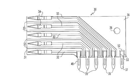
Referring to Figure 2, the PCB assembly 30 comprises an insulating
substrate 31 of a material commonly commercially used for making PCBs.
The substrate 31 can be a resin impregnated fiber material, such as is
CA 02225151 1997-12-17
11 E L-6158
sold under the designation FR4, having a thickness 0.4 mm, for example.
On a first surface of the substrate 31, a plurality of signal traces 32 are
formed by conventional PCB techniques. Each trace 32 extends from a
first portion of the substrate 31, for example adjacent the front edge as
shown in Figure 2, to a second area or region of the substrate 31, such as
the bottom edge as shown in Figure 2. The traces 32 include contact
pads at each end adapted to have metal terminals secured to them, as by
conventional surface mounting techniques using solder. A plurality of
ground or shielding traces 33 are also be applied to the substrate 31. The
shielding traces 33 are preferably disposed between each of the circuit
traces 32. A terminal, such as a contact terminal 34 is mounted at the
first end of each trace 32 and a connector mounting side terminal 35 is
mounted on the second end of each circuit trace 32. An additional
shielding or ground layer 36 may be applied to the remainder of the
substrate 31. A ground terminal 37 is fixed onto the ground layer 36, in
alignment with the terminals 35.
A locating hole 39 may be appropriately placed in the substrate 31.
The locating hole 39 preferably comprises a plated through hole for
establishing electrical connection with a grounding layer 38 (Figure 5)
that may extend substantially over the entire back surface of the
substrate 31. Small vias forming plated through-holes (not shown in
Fig.2) may be disposed in each of the ground tracks 33 so that the ground
CA 02225151 1997-12-17
err;
12 EL-6158
tracks 33, the shield layer 36 and the back shield layer 38 form a
shielding structure for the signal traces 32 and associated terminals. If
no shielding or limited shielding is desired, one or more of the shielding
structures 33, 36 or 38 can be eliminated.
As shown in the fragmentary views of Figures 3 and 4, contact
terminals 34 are formed as a one-piece stamping and can comprise a dual
beam contact having a base section 40 having an opposed pair of
upstanding portions 41. A spring section 42 is cantilevered from each of
the upstanding portions 41 to define an insertion axis for a mating
terminal, such as a pin from a pin header. Such a mating pin would
engage the contact portions 43 disposed at the end of each cantilevered
arm 42. The contact terminals also include a mounting section, such as
the planar member 44, that is adapted to be secured onto the end of the
circuit trace 32, typically by solder 46. The latter can be accomplished by
conventional surface mounting or other bonding techniques. As can be
realized by the above description, the cantilevered arms 42 and contact
portions 43 define a contact mating or pin insertion axis that is generally
parallel to the plane of substrate 31, but is offset from the surface
carrying the conductive traces 32.
As illustrated in Figure 5, one preferred form of connector mounting
terminal 35 includes a press-fit section 48 and a board mounting section
49. The board mounting section 49 includes a generally planar base 50
CA 02225151 1997-12-17
13 E L-6158
with an upturned top tang 52 disposed along a top edge. A pair of
opposed side tangs 53 are also upturned from the base 50. The mounting
portion 49 is retained on the circuit trace 32 by solder fillets 54, again
formed by conventional surface mounting solder techniques. Preferably,
the top tang 52 is spaced closely adjacent to or rests on the top surfaces
of the side tangs 53 as shown in Figure 5.
Figures 6, 6a, 6b, 6c and 6d illustrate an insulative cover/ spacer
member 56, preferably molded from an appropriate polymeric insulating
material. The cover includes a plurality of contact recesses 57 formed
along one edge. Each of the recesses 57 includes a contact preload rib
58. A large central recess 59 may also be formed in the cover. A second
plurality of terminal recesses 60 is formed along a second ede of the
cover. Further, a locating boss 62 is integrally formed with the cover and
is sized and shaped to be received, with limited clearance, in the locating
opening 39 in the substrate 31. The cover further includes an upper rim
63 extending from the rear of the cover to a location near the recesses 57.
A bottom rim or support member 64 is formed on a portion of the bottom
surface of the cover. The cover 56 further includes an upper locating and
mounting rib 65, preferably in the form of a dove tail rib as shown. A
similar but shorter mounting and locating rib 66 is disposed on the
bottom edge of the cover. The surfaces 67a and 67b form board rest
surfaces against which a substrate 31 is placed. The surfaces 67a and
67b may carry an adhesive or alternately a double sided adhesive coated
~w- CA 02225151 1997-12-17 ,~i
14 EL-6158
film (not shown) may be applied to extend from surface 67a to surface
67b.
It is noted that a half of one type of twinax contact module may be
formed by associating a PCB assembly 30 with a cover 56 to form a
module 69. Figure 7 is substantially an x-ray view through the cover 56
of column terminal module 69. For ease in showing the location of the
elements on substrate 31, with respect to features of the cover 56, the
conductive traces and terminals are rendered in full line rather than
phantom view. The PCB assembly 30 is located in the vertical direction
by the upper and lower rim or mounting members 63, 64 and is located in
a longitudinal manner by the locating boss 62 (see also Figure 7e). The
contact terminals 34 are located in the contact recesses 57 and the
connector mounting terminals 35 are located in the recesses 60. The
previously mentioned adhesive or adhesive coated films on surface 67a
and 67b maintain the PCB assembly and cover 56 together.
Figure 7a is a sectional view taken along line AA of Figure 7 and
shows the contact terminals 34 located 'in the contact recesses 57. The
terminals 34 are positioned so that the contact portions 43 bear against
the preload ribs 58 to impart a desired preload on the cantilevered spring
arms 42.
CA 02225151 1997-12-17
15 EL-6158
Figure 7b is a sectional view taken along line BB of Figure 7. As
shown in Figure 7b, the substrate 31 is essentially located in a vertical
position by the rims 63 and 64.
As illustrated in Figu: a 7c, each connector mounting terminal 35
has its mounting portion received within a corresponding recess 60. If
the board mounting terminal is of a type that is likely to have a relatively
high axial force applied to it, such as a press-fit terminal, the surface 68
(Figure 6d) of the recess 60 is advantageously located so that it bears
against the upturned tang 52 of the terminal. The views in Figures 7c
and Figure 9 (discussed below) are taken substantially along section line
cc of Figure 7.
Figure 7d is a fragmentary cross sectional view taken along line DD
of Figure 7, showing the positioning of grounding terminal 37 in a similar
fashion to terminals 35 shown in Figures 7c and Figure 9 (discussed
below) .
Figure 7e is a view of the back end of the module 69 showing in
phantom views the locating boss 62 and the mounting portion of
terminal 37.
Figures 8 and 8a illustrate enlarged views of the connector contacts
34 located in recesses 57 of the cover 56. Figure 8a is a cross sectional
view taken along line GG of Figure 8 and shows the positioning of the pre-
load rib 58 with respect to the contact portions 43.
CA 02225151 1997-12-17
16 E L-6158
Figure 9 illustrates the interaction of the cover 56 with the board
connection terminal 35 when a downward force F is applied to the top
edge of the module 69. That force is transmitted by the cover to the
pressing surface 68 formed by the top surface of the recess 60. As a
result, a vertical insertion force that is used to push the press-fit 48
section into the hole T is applied directly to the upper tang 52 and the
side tangs 53. In this manner, shear stress occurring at the solder
connection between the base 50 of the terminal and the circuit trace 32 is
minimized. In this manner, loosening or detachment of the terminal 35 is
avoided. This is achieved, at least in part, by positioning the surface 68
so that it will engage tang 52 before the rim 63 begins applying a vertical
force to the upper edge of the substrate 31. One way to accomplish this is
to provide an initial, small clearance between the rim 63 and the adjacent
edge of substrate 31. Additionally, the cover is designed so that a
significant proportion of the insertion force is applied directly to terminal
35 so that stress at the terminal/conductive track interface is minimized.
The structure disclosed is designed to withstand required press-fit pin
insertion forces of 35-50 Newtons per pin.
Figure 10 is a cross sectional view taken along line HH of Figure
l0a and shows a connector housing 70 having a top wall 72, a bottom
CA 02225151 1997-12-17
17 EL-6158
wall 76 and a front wall 78. The top wall 72 includes a plurality of
locating slots, for example the dove tail slots 73. One or more guiding
ridges 74 may be formed on a top surface of the top 72. The bottom 76
also includes locating slots, for example the dove tail slots 77. The front
wall 78 includes a plurality of openings 79. Additional shielding can be
provided by metallizing appropriate surfaces of the housing 70. Figure
lOc shows a bottom view of the housing 70 shown in Figure 10.
Figure 11 is a front elevational view of a lead-in face plate 80 having
a plurality of tapered lead-in sections 84 arranged in the form of a grid.
Each of the lead-in portions 84 extends to a pin insertion port 85. A
plurality of sleeves or hollow bosses 86 extend from the rear surface of the
face plate 80 and are shaped and sized to be positioned and retained in
the openings 79 in the front wall 78 of housing 70. The use of a separate
lead-in plate is desirable when the interior surfaces of the housing 70 are
to be fully metallized. However, the housing 70 can also be formed with
the lead-in plate integrally molded, where selective metallization or no
metallization is utilized.
Figure 12 illustrates printed circuit board modules configured to
provide connectors having shield pairs of terminals. The module 30
shown in the lower portion of Figure 12 is essentially the same as the
module illustrated in Figur° 7 wherein the dotted lines illustrate the
location of structures on the side of cover 56 located on the reverse side of
CA 02225151 1997-12-17
y
18 EL-6158
the cover adjacent PCB 31 (Figure 7C). For purposes of clarity, traces 32
and 33 have been shown in full line rather than dotted or phantom form.
The elements forming the module 30 are the same as those discussed in
connection with Figures 2 - 9 and no further description thereof is
believed necessary. PCB module 30~ includes essentially the same
elements as module 30 and these have been designated by the
designation. Module 30' differs from module 30 essentially in the aspect
that the elements of this module are arranged to constitute a mirror-
image with a respect to line L.
Figure 13 illustrates a generalized cross-sectional view of modules
30 and 30'arranged in back to back relationship to form a complete
shielded pair module that can be placed in side by side relationship with
similar modules to form a connector. In this arrangement, the back
shielding layers 38, 38~ of the PCB's 31, 31' are arranged adjacent one
another to form the shielded pair module. The modules 30, 30' can be
held in the illustrated relationship by insertion into housing 70 (Figure
10) or, if desired, by a conductive adhesive layer applied to adjacent outer
surfaces of shielding layers 38, 38'. In the shielded pair modules shown
in Figure 13, the dimension X represents the centerline distance between
the terminals 34 and 34~, which essentially constitutes the contact pitch
between the terminals. The dimension A represents the overall thickness
of the shielded pair module. As illustrated, the dimension A is twice the
thickness of one of the PCB modules 30, 30. Preferably, the dimension A
CA 02225151 1999-09-30
19
is chosen so that the terminal pitch X is maintained between adjacent
shielded pair modules. Referring to Figure 14, spacers 90 having a thickness
represented by the dimension B may be placed between PCB modules 30
and 30' to achieve a desired terminal pitch X.
Figure 15 is a rear view of a completed 5 x 6 connector (rows x
columns) formed by juxtaposing three shielded pair modules arranged in side
by side relationship within housing 70. Each module 90 includes a pair of
juxtaposed PCB's 31, 31' on which press-fit terminals (such as shield
terminals) 37, 37', are mounted. Each PCB 31, 31' is held by an
associated insulative cover 56, 56'. The covers 56, 56' have dove-tail ribs
65, 65' fitted within dove-tail slots 73 in the housing. The dotted squares
92 represent the locations of the terminals 34, 34' and generally
correspond to the location of the openings 85 in the face-plate 80 (Figure
11 ). The contact pitch X existing between adjacent columns at the
intermating face of the connector also exists at the board mounting
interface at terminals 37. Each of these shielded pair modules 90 carry
five shielded pairs of terminals and terminal leads in the 5 x 6
configuration illustrated in Figure 15.
Figure 16 is a rear view of a connector essentially as illustrated in the
aforementioned PCT application WO 97/02627. In this arrangement, the
PCB modules 30 are arranged in the connector housing 70 so that all of the
PCB assemblies 30 are oriented in the same way, for example, with the cover
56 disposed on
i CA 02225151 1997-12-17
20 EL-6158
the left-hand side and the PCB 31 disposed on the right-hand side. This
results in a connector having each terminal being substantially fully
electrically isolated from all others in the connector. For comparison,
Figures 17a, 17b, and 17c illustrate connectors embodying an aspect of
the present invention. Figure 17a illustrates from a rear view one form of
twinax connector having shielded pairs of terminals and terminal leads.
This arrangement differs essentially from that shown in Figure 15 by
having the relative positions of the covers 56, 56~ and PCB's 31, 31~
reversed. In this connector, the terminal pair modules 91 are formed by
placing the covers 56, 56~ in back to back relationship with the PCB's 31,
31 ~ forming the exterior surfaces of the module. In this arrangement, the
signal and ground traces 32, 32~ and 33, 33', respectively are located in
facing mirror-image relationship on the interior surfaces of the PCB's 31,
31 ~, with the outer-shielding layers 38, 38' disposed outwardly. Such an
arrangement forms twinax pairs 93 of terminals that are substantially
parallel through the conductor and have essentially identical electrical
characteristics. These pairs are shown by the dotted enclosures 93 for
the left-hand most module 91. The connector shown in Figure 17b is
essentially the same arrangement as that shown in Figure 17a, with the
exception that instead of two covers 56, 56~, a single insulative member
57 is utilized to hold the opposed PCB's 31, 31'. In each of the modules
91 the outer surfaces of the member 57 are configured similarly to the
interior surfaces of the covers 56, 56~. Figure 17c essentially illustrates
CA 02225151 1997-12-17 y
21 EL-6158
the arrangement previously discussed with respect to Figure 15. Instead
of using two PCB's, a single multi-layer PCB 3l~~may be employed having
a centrally located, substantially continuous central shield layer, with the
signal and shielding traces formed on opposed sides of the 31-'in mirror-
image relationship.
Figures 18a and 18b are schematic representations designed to
illustrate the electrical differences between the Figures 17a-b type of
connectors and the Figure 17c type of connector. Referring to Figure 18a,
the pair of interconnection terminals 94 are electrically isolated by a
common shield S. Whereas, in Figure 18b each of the interconnections
94 of the pair are individually shielded. In either case, an electrically
matched pair of interconnections are formed to maintain essentially a
twinax relationship through the interconnection.
The foregoing descriptions have been in the context of connectors
that are attached to printed circuit boards. Figure 19 illustrates an
arrangement for cable connectors. Figure 19 shows a cover 100 for use
with a circuit board generally of the type previously described. The upper
portion of the cover 100 is substantially~similar to the cover 56 shown in
the previous embodiments. It includes on its upper and lower surfaces
dove-tail ribs 165 and 166 that are designed to be received in
corresponding dove-tail grooves in. a housing, such as housing 70 shown
in Figure 10. A printed circuit board has a plated through hole for
CA 02225151 1997-12-17
22 EL-6158
receiving the locating lug 162. The locating ribs 163 and 164 are the
equivalent of locating ribs 63 and 64 shown in Figure 6C and serve to
locate the PCB in the same manner. The PCB assembly to be associated
with the cover 100 differs from those previously described essentially by
the absence of press-fit terminals 35 and 37.
The cover 100 includes a retaining structure 102 for retaining a
flexible conductor, for example, a cable formed of a plurality of individual
wires. The retaining structure 102 includes an opening 104 for receiving
the cable. A suitable strain relief element or elements may be provided at
the location of opening 104 to enhance cable retention. The retaining
structure 102 preferably includes a plurality of routing pegs 106 that are
useful to separate individual wires that are to be attached to the PCB.
Such individual wires are schematically illustrated by the dotted lines 108
in Figure 19. The ends of the wires 108, 109 may be soldered to contact
pads on the PCB that are coincident with the recesses 110 in the cover
100. Subsequent to soldering the wires 108, 109 to the PCB, the PCB is
assembled to the cover 100 and the individual wires 108 are arranged
between the pegs 106. If the cable (not shown) includes one or more
drain lines, which can be represented by the line 109, these drain lines
can be soldered to the shielding structures of the printed circuit board
such as traces 33, layer 36 and 38 by connection at an appropriate
location, for example, the right hand at most location of the PCB that in
CA 02225151 1997-12-17
. 23 EL-6158
the previous embodiment corresponds to the location of press-fit shield
terminal 37. For twinax cable connectors, shielded pair modules employ
two covers 100, one of which is a mirror-image of the other. Each one of
a twisted wire pair is connected to corresponding traces on each of the
printed circuit boards.
If each twisted pair has an individual drain, the drain wire can be
connected to an appropriate shielding trace 33.
Figures 20a - 20c illustrate the components of a typical cable
connector. The connector illustrated is a twinax connector but other
configurations are possible by varying the relative orientation and layout
of the modules. In this connector there are two mirror image PCB's 31
and 31 ~ placed in back to back relationship with shielding layers placed
next to each other. Signal wires 108 are each attached to one of the
conductive signal traces 32 on each of the PCB's 31 and 31 ~, along a
bottom edge of each PCB. In a twinax connector, conductors from each
twisted pair would be attached to corresponding signal traces on each of
the PCB's 31 and 31 ~. If a drain or shield 109 is present in the cable, it
can be secured to the shield portion 36 : The securing of the various
wires to the PCB's is accomplished by conventional means, such-as
soldering or welding.
The shield traces 33 and shield portion 36 are interconnected to the
shield layers 38 and 38' by plated vias 112 and the plated location hole
39 as previously described. Covers 100 and 100' are secured onto the
;CA 02225151 1997-12-17
24 EL-6158
respective PCB's 31 and 31 ~. The retainer sections of each cover
surround the ends of the wires attached to the PCB's 31 and 31'. The
retaining sections include the pegs 106, which provide strain relief and
wire support functions.
The PCB's 31 and 31 ~ may be held together by a conductive
adhesive or may be closely held together by the effect of the dove tail ribs
165 and 165 and corresponding dove tail slots 73 and 77 in the housing
70, as the module is assembled in the housing 70 as shown in Figure
20b. A plurality of modules are arranged in the molded plastic housing
70, the interior surfaces of which may be metallized to provide additional
shielding. The face plate 80 is secured to housing 70 to form the
completed right angle cable connector shown in Figure 20c.
Figures 21a - 21c show essentially the same elements illustrated in
Figures 20a - 20c with the exception that the PCB's 33 and 33' are
configured to provide a cable connection end at the rear edge of the PCB's
rather than the bottom edge. The insulating covers 100 and 100' are
modified correspondingly to situate the cable retaining sections 102 and
102 at the rear edges of the PCB's. The covers include pegs 106 for
providing support, organization, and strain relief. The covers 100 and
100' may be secured together at engaging edges along the PCB's and at
the retaining sections, for example by adhesives or solvent or heat
welding.
CA 02225151 1997-12-17
25 EL-6158
The modules are then inserted into housing 70 as shown in Figure
21 b and are retained in the housing as previously described. A completed
straight connector is formed by the insertion of a plurality of modules in
side by side relationship into the housing 70 and securing a face plate 80
on the housing, as illustrated in Figure 21c.
The foregoing constructions yield connectors with excellent high
speed characteristics at relatively low manufacturing costs.
While the present invention has been described in connection with
the preferred embodiments illustrated in the various figures, it is to be
understood that other similar embodiments may be used or modifications
and additions may be made to the described embodiment for performing
the same function of the present invention without deviating therefrom.
Therefore, the present invention should not be limited to any single
embodiment, but rather construed in breadth and scope in accordance
with the recitation of the appended claims.