Note: Descriptions are shown in the official language in which they were submitted.
CA 02225219 1997-12-18
577-212
ELECTRICAL CONNECTOR WITH PIN RETENTION
FIELD OF THE INVENTION
The present invention relates generally to electrical connectors. More
specifically, the
present invention relates to a pin retention means employed in an electrical
connector.
BACKGROUND OF THE INVENTION
The use of mufti-contact connectors is a well-known method for providing an
organized
and orderly connection of multiple leads such as in electronic devices. Mufti-
contact connectors
terminate conductors and cables between electronic circuits within a system,
between systems,
and between systems and external power sources and signal lines. Mufti-contact
connectors
interconnect circuits on circuit boards with backplanes or backpanels or
wiring within an
enclosure. They may also interconnect chassis and circuit boards in different
enclosures.
Such connectors come in a variety of shapes including trapezoidal,
rectangular, and
circular. These connectors typically include an electrically insulative
connector housing
containing multiple apertures through which conductive connector contacts are
inserted. These
connector contacts, a plurality of which are included in such connector
assemblies, are connected
to separate incoming wires and a dielectric insert assembly for fixedly or
removably mounting
the electrical contacts in the connector shell.
For example, right angle, D-faced electrical connectors are used in the
electronics
CA 02225219 1997-12-18
industry as input/output devices to interconnect a computer to external
peripheral equipment.
The contacts of the electrical connector are typically soldered to conductive
traces on a printed
circuit board at a backwall or panel of the computer. The front face on the
connector is mated
with a complementary electrical connector which is attached to the peripheral
equipment.
S
These types of electrical contacts are supported in apertures in the
insulative housing of
the connector with back ends of the contacts bent at right angles. The
contacts terminate in
solder posts which extend downward from the connector housing for insertion
into through-
plated holes in a printed circuit board for subsequent soldering thereto.
Typically the contacts are held in place by an interference fit between the
contact and the
wall forming the aperture in the connector housing by either oversizing the
contact to the
aperture or by providing barbs on the contact which engage the internal wall
defining the
aperture.
However, by employing an interference fit between the contacts and the
connector
housing, several problems are commonly experienced. One such problem is that
the insertion fit
can cause warpage of the connector housing. Also, the insertion forces
required to insert contact
pins through the connector housing can sometimes bend, misalign, or skew
either the pins or the
solder tails. As mentioned above, because of the importance of properly
aligning the solder tails
to the appropriate terminal in the printed circuit board, such misalignment
can render a connector
unusable.
2
CA 02225219 1997-12-18
Furthermore, interference fit connectors require a precise fit between the
hole and contact
in order to eliminate some of the above-mentioned problems. This necessitated
the use of tight
tolerances which increased production costs.
U.S. Patent No. 5,017,159 discloses an electric terminal for mounting
electrical
components on printed circuit boards. A mounting leg is employed to secure the
connector to the
printed circuit board. This mounting leg includes at least one elongate
indentation in the
mounting end parallel to the longitudinal axis which facilitates the splitting
of the mounting leg
along the indentation into two half leg portions and splaying the two half leg
portions into
abutment against the opposed side of the printed circuit board to secure the
position of the
terminal on the printed circuit board. However, it has been found that in some
cases splaying
does not follow the coin along the center of the leg, but favors one side and
results in an
asymmetrical one sided splay. Such off center splaying has a tendency to
further pull the
terminal pin off the original center line perpendicular to the printed circuit
board surface.
SUMMARY OF THE INVENTION
It is an object of the present invention to provide an electrical connector
which
insulatively supports contacts within a connector housing.
It is also an object of the present invention to provide an electrical
connector where the
contacts can be easily inserted into the connector housing without change to
the contacts or the
housing.
3
CA 02225219 1997-12-18
A further object of the invention is to provide a connector where the contacts
are easily
inserted into the connector housing which thereby eliminates misalignment of
the pins or solder
tails by the high insertion forces of the prior art.
In order to achieve these and other objectives, the present invention
comprises an
electrical connector comprising an insulative housing having an elongate
aperture therethrough.
An elongate electrical contact is insertable within said housing aperture in a
direction of
insertion, said contact having a first end extending externally through a
first end of said aperture,
and an opposed second end extending externally through a second end of said
aperture. The
contact further includes a deformable flange adjacent the first end of the
contact for expanded
deformation so as to prevent removal of said contact from said housing
aperture in a direction
opposite said direction of insertion.
The present invention also comprises an electrical connector comprising an
insulative
housing having a connection face and an opposed termination face, and a
plurality of elongate
apertures extending between the connection face and the termination face. Also
included is a
plurality of mated elongate electrical contacts insertable within said housing
from said
termination face to said connection face. The contacts have first ends
extending externally
through first ends of said apertures, and opposed second ends extending
externally through
opposed second ends of said apertures. The contacts further include a
deformable flange
adjacent said first end of the contacts for expanded deformation so as to
prevent removal of said
contacts through said termination face.
4
CA 02225219 1997-12-18
BRIEF DESCRIPTION OF THE DRAWINGS
Figure 1 is an exploded view of a connector for employing the contact
retention method
of the present invention.
Figure 2 is an isometric view of a connector employing the contact retention
of the
present invention.
Figure 3A is a cross-sectional view of the connector of Figure 1 where the
drawing shows
the insertion of the contacts into the connector housing of the present
invention.
Figure 3B is a cross-section view detailing a fully inserted contact in the
connector
housing of the present invention.
Figure 3C is a cross-section view showing the swaging of the contacts inserted
into the
connector of the present invention.
DETAILED DESCRIPTION OF THE INVENTION
The present invention provides an electrical connector which supports a
plurality of
contacts in a housing unit within a mated aperture. The electrical contacts
are retained in a
receiving aperture by the expansion of a deformable flange portion of the
contact once the
contact is inserted in the aperture.
5
CA 02225219 1997-12-18
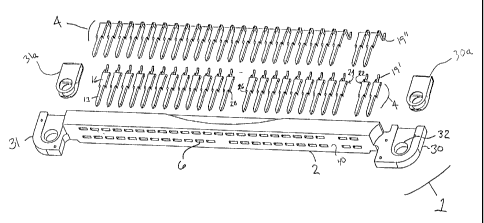
As shown in Figures 1 and 2, the present invention provides an electrical
connector 1 for
establishing electrical connection between a mating electrical connector (not
shown) and a
printed circuit board (also not shown). In a preferred embodiment, electrical
connector 1
includes a connector housing 2, which is a generally elongate rectangular
member, fabricated
from an electrically insulative material such as molded plastic. Housing 2
includes a plurality of
apertures 6, which are generally rectangular in shape, through which the
contacts 4 are inserted.
The apertures 6 may be arranged in two longitudinally extending transversely
spaced rows, as
shown. However, other aperture shapes and arrangements of apertures are within
the
contemplation of the present invention.
The contacts 4 are elongate members typically stamped from a planar sheet of a
conductive metal. The contacts 4 each include an elongate interconnection end
in the shape of a
pin 13, an opposed surface mount solder tail 19, and a central body 16
therebetween. While pins
13 and solder tails 19 are shown in the preferred embodiment, the
configuration of contacts 4 is
not limited thereto. Contact body 16 is an elongate flat planar member having
extending
shoulders 22, and 24 adjacent solder tails 19 and deformable retention flanges
26 and 28 adjacent
pin 13
Depending on the spacial relation and orientation between a particular contact
4 in the
connector housing and the preferred location for connecting the corresponding
solder tail 19,
solder tail 19 may be a straight member or it may be bent into a configuration
that provides
connection of the solder tail 19 to a lead spaced away from the connector 1.
Figures 1 and 2
6
CA 02225219 1997-12-18
show examples of a straight solder tail 19" which allow connection leads in a
single plane as
provided, for example, by a printed circuit board. While the figures show the
contact with one
end leading into a solder tail, this is not the only construction contemplated
by the invention.
As shown in Figures 1 and 2 contacts 4 are positioned within housing 2 so as
to permit
electrical connection between contacts of a mating connector and traces on a
printed circuit
board. Pin 13 extends externally of a connection face 40 while solder tail 19
extends externally
of an opposed termination face 42. As is well known in the connector art, pins
13 are designed
for mating interconnection and solder tails 19 are designed for solder
termination to a printed
circuit board.
Figures 3A-3C provide a cross-sectional view of a portion of connector housing
2. The
apertures 6 are formed to cooperatively receive the contacts 4 inserted
therethrough. Apertures 6
are elongate apertures defined between connection face 40 and termination face
42. Opposed
side walls 11 and 12 of housing 2 further define aperture 6. The apertures 6
include recesses 7
and 8 at each longitudinal end thereof, namely connection face 40 and
termination face 42
respectively.
Recess 7 is defined by a recessed surface 9, and is in communication with
termination
face 42. Recess 7 has a width which is greater than the width of a central
portion 6a of aperture
6.
Recess 8 is defined by tapered walls 11 c and 12c which open outwardly to
connection
7
CA 02225219 1997-12-18
face 40. Tapered walls 11 c and 12c form a recess of increased width at
connection face 40 which
will engagingly receive deformable flanges 26 and 28 for retention.
While both the central contact body 16 and the receiving aperture 6 have been
displayed
in a rectangular shape, the invention is not limited to the rectangular shape,
as other varieties of
shapes are contemplated.
Contacts 4 are generally inserted into housing 2 from the termination face 42
towards the
connection face 40 in the direction of arrow A. The contacts 4 are of such a
dimension with
respect to apertures 6 that free unrestricted insertion is permitted.
In the preferred embodiment shown herein, as the apertures 6 and contact body
16 of
contacts 4 are both generally rectangular in cross-section, the shape and fit
between contact body
16 and aperture 6 within connector housing 2 prevents the rotation of the
contacts 4 about their
longitudinal axis Y. The contacts 4 are inserted until the leading edges 23
and 25 of shoulders 22
and 24, which are wider than the contact body 16, cooperatively engage and
seat against recessed
surface 9. Such seating provides a mechanical stop and prevents over-insertion
of the contacts 4
in housing 2. In this position, deformable retention flanges 26 and 28 are
positioned so that the
pin 13 extends fully through connector face 40 as shown in Figures 3B and 3C.
Figure 3B
shows that once contact 4 is fully inserted into aperture 6, deformable
retention flanges 26 and 28
are positioned adjacent to tapered walls l lc and 12c.
CA 02225219 1997-12-18
Referring to Figure 3C, deformable retention flanges 26 and 28 may be swaged
outwardly
to abut tapered walls 11 c and 12c. An appropriate tool 25 may be used to
simultaneously swage
both deformable retention flanges 26 and 28. The swaged retention flanges 26
and 28 thus reside
against recess 8, to thereby lock contact 4 within the connector housing 2.
The contact 4 is thus
longitudinally confined by a retention force acting through contact 4 at
flanges 26 and 28
adjacent connector face 40, and at shoulders 22 and 24 adjacent termination
face 42.
Swaging the connector contacts 4 into place within the connector housing 2
provides a
high retention force for maintaining contacts 4 within the connector housing
throughout the
lifetime of the connector. The high retention force provided by the present
invention is obtained
with a relatively low deformation force being applied to the deformable
flanges 26 and 28. Thus
the present invention allows the contacts 4 to be easily inserted into the
connector housing 2
which eliminates misalignment of the pins 13 or solder tails 19 by the high
insertion forces
required by the prior art.
Because the present invention does not rely on an interference fit between the
contacts 4
and the aperture 6 within connector housing 2 to maintain the contacts in
place, the present
invention also eliminates warpage caused by the interference fit of each
contact with the
connector housing.
Furthermore, in the present invention, the contact is not skewed in its
entirety, which
leads to unequal distribution on either side of the skewing and an off balance
resulting
9
CA 02225219 1997-12-18
connection. The off balance connection causes subsequent misalignment with
printed circuit
boards and results in a unusable electrical connector.
Figures l and 2 also illustrate connection ears 30 and 31 extending from
housing 2 at
S each end thereof. Connection ears 30 and 31 provide for the securing of
connector 1 to a circuit
board so that the load is not borne by the solder tails 19. The ears 30 and 31
include mounting
brackets 30a and 31a equipped for receipt of appropriate mounting hardware
(not shown). The
attachment of connector 1 to the printed circuit board may also be attained by
other means well
known in the art.
The present invention is intended to conform to the preceding description but
is not
limited thereto. In addition to those instances mentioned above which may
deviate from the
description, the shoulders of the contacts and the recessed surfaces against
which they abut need
not be limited to a rectangular shape.
10