Note: Descriptions are shown in the official language in which they were submitted.
CA 02225320 1997-12-19
W O 97!39605 PCT~B97/00260
Circuit arrangement.
The invention relates to a circuit arr~n~P-ment for i~niting and ope.~Ling a
high~ e discharge lamp, provided with
- input tPrmin~1~ for co~lne~ n of a supply source,
- output terrninals for co~-n~l;o~ of the larnp,
- switching means for o~ ;Qi'. the lamp a~ a nominal lamp voltage Vla during
stable lamp opP~tion and for genP~ting an open voltage Vo at the output
termin~l~ before the lamp has i~nitP~,
- ignition means for ~,ene~l-nf~ an igni~ n voltage pulse when the voltage at the
output terminals reaches a threshold value Vi,
- a control circuit for controlling the switching means.
Such a circuit arrangement is lmown ~rom EP 0401931 = US 5,068,572).
The known circuit ~ldnge"lent is suitable for igniting and operating inter alia high-ples~ule
15 sodium lamps and metal halide lamps. These lamps are in general provided with a discharge
vessel in which an electric disch~;e is ...~ ed during operation and which is çncl~spd
with intervening space by an outer bulb. These lamps require a high in~ition voltage pulse (a
few kV and more). The ignition means become operative through the choice of the open
voltage Vo such that Vo > Vi, and an ignition voltage pulse is g~ "nled. The lamp will
20 ignite then, the voltage across the lamp dropping abruptly to around ten volts. As soon as a
stable discharge has arisen in the lamp, the voltage across the lamp gr~ tly ri~s up to the
lamp voltage Vla accol,lpa~lying stable lamp operation. The circuit ~rr~ngem~nt is so
deci~nPd that the lamp voltage Vla is lower than the voltage Vi, which in its turn is lower
than the open voltage Vo.
The control circuit of the circuit ~n~ngPntPnt ensures that the switching
means act as a controlled current generator in the stable op~tiQnal state of the lamp. It is
achieved thereby that no more iEniti~n voltage pulses are geneldled by the iEr it;o~ means as
soon as the voltage at the connectit)n terminals drops to the lamp voltage Vla or lower.
The ge~ on of igrlition voltage pulses for a longer period is
CA 02225320 1997-12-19
WO 97!39605 2 PcT~B97loo26o
undesirable because this forms a load on the circuit ~rrang~pmpnt It is often suE~est~d in the
dLul~, therefore, to limit the operation of the i~nitit)n means by switching them off after a
cert~un period has elspsP~.
This, however, has a number of disadvantages:
S - the ~~ ely high open voltage Vo ~ ,ains at the output terminals if the
lamp has not yet ignited,
- once the lamp has ignitP~, the iEnition means will generate i~nition voltage
pul~s the mom~nt the lamp is extinguished, for eY~mple upon re~rhin~ the end
of its oper~ti~n~l life. R~ ly high-pressurG sodium lamps and metal halide
lamps show the chaMctPri~tir that the lamp will ignite again upon the
application of ignition voltage pul~s at the end of its life after eYtin~ hin~
and cooling-down. This gives rise to the char~ctPri~tic fli-~1rPrin~ behavior of the
lamp. This is I ~p'~ rlt to ob~rve, but most of all it is ~lel . ;~..e~,t:.l to the
circuit ~ldl g~lnGn~, while it usually also leads to a con~i~p-~hle ~mount Of
i~ re.e.-ce r~ tion (radio i.~tc.ÇelGnce, etc.).
The invention has for its object to provide a measure for counte..-cting the
above disadvantages.
According to the invention, a circuit arr~ngeln~nt of the kind mentiQn~ in
the opening paragraph is for this purpose ch~ractPrized in that the control circuit comprises
means for 1imiting the voltage at the output terminals to a value Vb such that the following is
true
Vla < Vb < Vi.
The choice of the voltage at a level just above the nomin~l lamp voltage
adv~nt~ o~ly reali~s that the generation of i~nition voltage pulses is su~,~ssed by one
and the same ,~h~n;sm both in the case of a badly starting lamp and in the case of a lamp
which reaches the end of its life. A further advantage is that a discharge in the outer bulb of
the lamp, either in the form of a glow discharge or in the form of an arc disch~ e, cannot
30 be ...~ .~l when the discharge vessel of the lamp becomes leaky, so that hazardous
situ~tions are prevented. A particularly suitable embodiment of the means for limitin~ the
voltage at the output terminals comprises a timer which after a preset time interval brings the
control circuit into a state such that the voltage oc-iu~ at the output l~."inals is limited to
the value Vb. Preferably, the timer is so co~ne~t~d that it is reset upon connection of a
CA 02225320 1997-12-19
W O 97!39605 3 PCTnB97/00260
supply source. l~er~àbly~ a voltage buffer network is coupled to the timer in order to
prevent the timer from being reset also in con~1itionC where there is a short dip in the supply
voltage delivered by the supply source. This network may be, for example, an RC netwc.,k.
A dow"~-,re.L. or Buck con~e.~r is very suitable for use as the controlled current
S genclator.
The above and further aspects of the imvention will be ~ ;n~ in more
detail below with l~f~,~ce to a drawing of an embo-~imPnt of a circuit accol.lillg to the
10 invention, in which
Fig. 1 shows a circuit arrangement for i~niting and o~.,~l;ng a high
.c; fii~ e lamp,
Fig. 2 shows switching means of the circuit ~ ngem~nt of Fig. 1 in
detail,
Fig. 3 shows means for limiting the voltage at the output terminals of the
circuit ~ ge-e-nt in more detail, and
Fig. 4 shows an embodiment of the means of Fig. 3 in further detail.
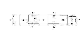
Fig. 1 shows a circuit alla~lge---ent for igniting and o~f~dling a high-
ple~:iUle discharge lamp, provided with
- input t~nnin~lc 1 for conn~ting a supply source,
- output terminals 2 for c~n.lP.~ g the lamp 3,
vilching means II for ope,dling the lamp at a nominal lamp voltage Vla during
stable lamp operation and for gene~ting an open voltage Vo at the output
inals before the lamp has ignited. The circuit ~l~lng~ nt is also provided
with c~ or means III for periodically rh~nging the ~ol~iLy of the current
through the lamp, and with a preco~lition~r I for gc~ ing a DC voltage for
supplying the switching means II. The coml~lu~tor means also col~ ise ignition
means ~not shown in any detail) for genel~Ling an ingition voltage pulse when
the vol~age at the output tPrmin~l~ reaches a threshold value Vi.
The circuit arr~n~eml~nt is further provided with a control circuit IV for controlling the
chi-lg means, and with means V for limiting the voltage at the output termin~lc to a value
Vb such that it is true that
CA 02225320 1997-12-19
W 097/39605 4 PCT~B97/00260
Vla < Vb < Vi.
In an advantageous emb~impnt~ the switching means are constructed as a
downconverter or Buck converter as shown in detail in Fig. 2. In ~ig. 2, A and B are
conn~tion points between the switching means and the precon~ition~r I, and C and D are
S C~nn~Ctioll points with the com~ tc" means III. The downconverter comprises a controlled
semico~A~ct~r switch 10, a self-induct~n~ 11, and a freewheel diode 12. The converter is
further provided with a c~u~ r 13 for red~lcing ripple on the voltage across the connection
points C, 1~. A control electrode 101 of switch 10 is conn~ted to an output 41 of the control
circuit IV. The control circuit has an input 42 for ~etect;ng a signal Sv which is p,~,po-Lional
10 to the voltage at the output terminals and an input 43 for cle~e~t;.-g a signal Si which is
p,~ lional to the lamp current and is formed over a small preferably ohmic in~l,edance Z.
The signal Sv is co,~alcd with a lcrelcncc voltage Vref. The result of this co.l.~ ison is
con-lllct~ to a gate controller 45. The signal Si is conduct~ through an il~t~gr;.tor 44A to
Pulse Width h~ocllll~tQr (PWM) 44, which in its turn sends a swi~l~ g signal to the gate
15 controller 45. The control signal gcn~ d in the gate controller 45 is conducted to the
control electrode 101 through output 41.
The rcrer~nce voltage Vref forms part of the means for limiting the
voltage at the output terminals to a value Vb such that it is true that
Vla c Vb < Vi.
The means V are shown in more detail in Fig. 3. The reference voltage
Vref is formed at connection point 52 from an auxiliary voltage Vh by means of a voltage
divider l,el~volk 50. A switch 51 is in~ n~ l in a branch of the voltage divider n~,lwcll~ 50
which is conn~tecl to conn~;~ion point 52 at one side. The switch 51 shunts a portion of the
im~ n~ bel~n~ing to the voltage divider network. In the embodiment shown, the switch is
25 accommnrl~ted in a branch b~w~n conne~tinn point 52 and ground. When the switch is
closed, the result will be a lower voltage at com eclion point 52 cor-Lpa-ed with the ~itll~tiOI~
of an opened switch. When the switch is placed between the voltage Vh and connection point
52, a re~uction in the voltage at cQIm~tion point 52 will take place when the switch 51 is
opened. A low voltage at connection point 52 means a low value for the reference voltage
30 Vref, which results in the gate controller 45 controlling the semiconductor switch such that
the voltage at the output t~rmin~l~ of the circuit arr~ngemP~lt is limited to a c~ p~dti~ely
low value. An çml~odiment of the means V as shown in Fig. 3 is d~ictçd in further detail in
~ig. 4. The switch is formed by a series arrangement of a diode 55, a timer 500, a voltage
buffer n e~ol~ 53, and a cnnn~tion point 54 for conne~ting a supply voltage for supplying
CA 02225320 1997-12-19
W O 9713960~ 5 PCT~B97/00260
the timer. The switch 51 operates as follows. The moment a supply voltage is connect~l to
coînn~ctinn point 54, a voltage will be applied to input terminal 501 of timer 500, whereby
the timer is reset. The result of this is that a high signal is present at an output terminal 502
of the timer. This co~ C to the state of a co~ dti~ely high voltage at conn~ion
point 52. After a period for which the timer was set has e1~rs~d the timer switches over and
the voltage at output terrninal 502 becomes low, so that the voltage at connection point 52
also beco.-les low.
In a practical re~li7~tio~ of a circuit ~ ngçm~nt accor~ing to the
embo~ t described, the circuit a l~lgel,lcnt is s~-it~hle for ignitins~ and O~ a metal
10 halide lamp, for PY~mple of the CDM 35W type, make Philips, with a power rating of 39
W. The lamp has a rated lamp voltage Vla of 90 V. When the supply source is conn~rt~
for eY~mple a voltage source of 220 V, 50 Hz, the pre~Qn-litionçr supplies a DC voltage of
400 V to the ~ ing means II. The open voltage at the output terminals lies b~t~n 310
and 380 V when the larnp has not ignited. The threshold value Vi of the voltage at the output
15 terminals at which the i~rlition means start gcl~c~dling iE,.;~ pulses is 240 V.
The timer 500 is formed by a type HI:F 4541 integ-~ted circuit. The
voltage buffer netwu,k 53 comprises a parallel amn~çme~t of a 100 nF c~p~ritor and a
zener diode with a zener voltage of 15 V. The rectified supply source voltage of 220 V
serves as the supply voltage for the timer circuit. To limit the current, a resistor of 300 kn is
20 co~ P~ i between connection point 54 and the voltage buffer network. Diode 55 is of the
BAV 103 type, make Philips. The value of Vref is 3.3 V when the timer is reset. When the
timer s~ilcl~es over after at most 20 min, Vref drops to 1.5 V, which results in a limit~tion
of the voltage at the output terminals to a value Vb of a~ most 200 V. It is clear that the
cQn~1ition
Vla < Vb < Vi
is thus complied with.
The timer is so set that it switches over after a minimll~n of 10 min and a maximum of 20
min. This time is pl~ rt;l~bly chosen to be so long to provide the possibility of hot re-i~nition
of the lamp. The controlled sen~i~n~ctor switch of the s~,vi~clling means is formed by a
MOSFET, type STP4NA60FI, make SGs-~homcon~ The gate controller is an i~)le~ P~l
circuit, type IR2117, make Int. l~tifier. The PMW 44 is an integ.aled circuit, type
L6560A, make SGS-Thomson.