Sélection de la langue

Search

Sommaire du brevet 2225320 

Énoncé de désistement de responsabilité concernant l'information provenant de tiers

Une partie des informations de ce site Web a été fournie par des sources externes. Le gouvernement du Canada n'assume aucune responsabilité concernant la précision, l'actualité ou la fiabilité des informations fournies par les sources externes. Les utilisateurs qui désirent employer cette information devraient consulter directement la source des informations. Le contenu fourni par les sources externes n'est pas assujetti aux exigences sur les langues officielles, la protection des renseignements personnels et l'accessibilité.

Disponibilité de l'Abrégé et des Revendications

L'apparition de différences dans le texte et l'image des Revendications et de l'Abrégé dépend du moment auquel le document est publié. Les textes des Revendications et de l'Abrégé sont affichés :

  • lorsque la demande peut être examinée par le public;
  • lorsque le brevet est émis (délivrance).
(12) Demande de brevet: (11) CA 2225320
(54) Titre français: MONTAGE ELECTRONIQUE
(54) Titre anglais: CIRCUIT ARRANGEMENT
Statut: Réputée abandonnée et au-delà du délai pour le rétablissement - en attente de la réponse à l’avis de communication rejetée
Données bibliographiques
(51) Classification internationale des brevets (CIB):
  • H05B 41/14 (2006.01)
  • H05B 41/18 (2006.01)
  • H05B 41/292 (2006.01)
(72) Inventeurs :
  • DEURLOO, OSCAR JAN
  • LAMMERS, FRANCISCUS HUBERTUS THEODORUS
(73) Titulaires :
  • KONINKLIJKE PHILIPS ELECTRONICS N.V.
(71) Demandeurs :
  • KONINKLIJKE PHILIPS ELECTRONICS N.V.
(74) Agent: SMART & BIGGAR LP
(74) Co-agent:
(45) Délivré:
(86) Date de dépôt PCT: 1997-03-17
(87) Mise à la disponibilité du public: 1997-10-23
Licence disponible: S.O.
Cédé au domaine public: S.O.
(25) Langue des documents déposés: Anglais

Traité de coopération en matière de brevets (PCT): Oui
(86) Numéro de la demande PCT: PCT/IB1997/000260
(87) Numéro de publication internationale PCT: IB1997000260
(85) Entrée nationale: 1997-12-19

(30) Données de priorité de la demande:
Numéro de la demande Pays / territoire Date
96201035.1 (Office Européen des Brevets (OEB)) 1996-04-18

Abrégés

Abrégé français

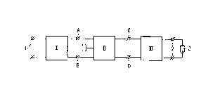
Cette invention porte sur un montage électronique permettant l'amorçage et la mise en fonction d'une lampe à incandescence à haute pression. Ce montage est constitué de bornes d'entrée pour connexion à une source d'alimentation, de bornes de sortie pour connexion à la lampe, d'un système de commutation permettant de faire fonctionner la lampe à une tension nominale (Vla), en fonctionnement stable, et de produire une tension à vide (Vo) aux bornes de sortie avant l'amorçage de la lampe, d'un système d'amorçage destiné à produire une impulsion de tension d'amorçage lorsque la tension aux bornes de sortie atteint une valeur de seuil (Vi) et d'un circuit de commande servant à commander le système de commutation. Le circuit électronique de cette invention se caractérise par le fait que le circuit de commande comporte des moyens permettant de limiter la tension aux bornes de sortie à une certaine valeur (Vb) de façon à ce que se vérifie la formule suivante: Vla < Vb < Vi.


Abrégé anglais


The invention relates to a circuit arrangement for igniting and operating a
high-pressure discharge lamp, provided with input terminals for connection of
a supply source, output terminals for connection of the lamp, switching means
for operating the lamp at a nominal lamp voltage Vla during stable lamp
operation and for generating an open voltage Vo at the output terminals before
the lamp has ignited, ignition means for generating an ignition voltage pulse
when the voltage at the output terminals reaches a threshold value Vi, a
control circuit for controlling the switching means. According to the
invention, the circuit arrangement is characterized in that the control
circuit comprises means for limiting the voltage at the output terminals to a
value Vb such that the following is true: Vla < Vb < Vi.

Revendications

Note : Les revendications sont présentées dans la langue officielle dans laquelle elles ont été soumises.


CLAIM:
1. A circuit arrangement for igniting and operating a high-pressure discharge
lamp, provided with
input terminals for connection of a supply source,
output terminals for connection of the lamp,
switching means for operating the lamp at a nominal lamp voltage Vla during
stable lamp operation and for generating an open voltage Vo at the output
terminals before the lamp has ignited,
ignition means for generating an ignition voltage pulse when the voltage at the
output terminals reaches a threshold value Vi,
a control circuit for controlling the switching means,
characterized in that the control circuit comprises means for limiting the voltage at the output
terminals to a value Vb such that the following is true
Vla < Vb < Vi.

Description

Note : Les descriptions sont présentées dans la langue officielle dans laquelle elles ont été soumises.


CA 02225320 1997-12-19
W O 97!39605 PCT~B97/00260
Circuit arrangement.
The invention relates to a circuit arr~n~P-ment for i~niting and ope.~Ling a
high~ e discharge lamp, provided with
- input tPrmin~1~ for co~lne~ n of a supply source,
- output terrninals for co~-n~l;o~ of the larnp,
- switching means for o~ ;Qi'. the lamp a~ a nominal lamp voltage Vla during
stable lamp opP~tion and for genP~ting an open voltage Vo at the output
termin~l~ before the lamp has i~nitP~,
- ignition means for ~,ene~l-nf~ an igni~ n voltage pulse when the voltage at the
output terminals reaches a threshold value Vi,
- a control circuit for controlling the switching means.
Such a circuit arrangement is lmown ~rom EP 0401931 = US 5,068,572).
The known circuit ~ldnge"lent is suitable for igniting and operating inter alia high-ples~ule
15 sodium lamps and metal halide lamps. These lamps are in general provided with a discharge
vessel in which an electric disch~;e is ...~ ed during operation and which is çncl~spd
with intervening space by an outer bulb. These lamps require a high in~ition voltage pulse (a
few kV and more). The ignition means become operative through the choice of the open
voltage Vo such that Vo > Vi, and an ignition voltage pulse is g~ "nled. The lamp will
20 ignite then, the voltage across the lamp dropping abruptly to around ten volts. As soon as a
stable discharge has arisen in the lamp, the voltage across the lamp gr~ tly ri~s up to the
lamp voltage Vla accol,lpa~lying stable lamp operation. The circuit ~rr~ngem~nt is so
deci~nPd that the lamp voltage Vla is lower than the voltage Vi, which in its turn is lower
than the open voltage Vo.
The control circuit of the circuit ~n~ngPntPnt ensures that the switching
means act as a controlled current generator in the stable op~tiQnal state of the lamp. It is
achieved thereby that no more iEniti~n voltage pulses are geneldled by the iEr it;o~ means as
soon as the voltage at the connectit)n terminals drops to the lamp voltage Vla or lower.
The ge~ on of igrlition voltage pulses for a longer period is

CA 02225320 1997-12-19
WO 97!39605 2 PcT~B97loo26o
undesirable because this forms a load on the circuit ~rrang~pmpnt It is often suE~est~d in the
dLul~, therefore, to limit the operation of the i~nitit)n means by switching them off after a
cert~un period has elspsP~.
This, however, has a number of disadvantages:
S - the ~~ ely high open voltage Vo ~ ,ains at the output terminals if the
lamp has not yet ignited,
- once the lamp has ignitP~, the iEnition means will generate i~nition voltage
pul~s the mom~nt the lamp is extinguished, for eY~mple upon re~rhin~ the end
of its oper~ti~n~l life. R~ ly high-pressurG sodium lamps and metal halide
lamps show the chaMctPri~tir that the lamp will ignite again upon the
application of ignition voltage pul~s at the end of its life after eYtin~ hin~
and cooling-down. This gives rise to the char~ctPri~tic fli-~1rPrin~ behavior of the
lamp. This is I ~p'~ rlt to ob~rve, but most of all it is ~lel . ;~..e~,t:.l to the
circuit ~ldl g~lnGn~, while it usually also leads to a con~i~p-~hle ~mount Of
i~ re.e.-ce r~ tion (radio i.~tc.ÇelGnce, etc.).
The invention has for its object to provide a measure for counte..-cting the
above disadvantages.
According to the invention, a circuit arr~ngeln~nt of the kind mentiQn~ in
the opening paragraph is for this purpose ch~ractPrized in that the control circuit comprises
means for 1imiting the voltage at the output terminals to a value Vb such that the following is
true
Vla < Vb < Vi.
The choice of the voltage at a level just above the nomin~l lamp voltage
adv~nt~ o~ly reali~s that the generation of i~nition voltage pulses is su~,~ssed by one
and the same ,~h~n;sm both in the case of a badly starting lamp and in the case of a lamp
which reaches the end of its life. A further advantage is that a discharge in the outer bulb of
the lamp, either in the form of a glow discharge or in the form of an arc disch~ e, cannot
30 be ...~ .~l when the discharge vessel of the lamp becomes leaky, so that hazardous
situ~tions are prevented. A particularly suitable embodiment of the means for limitin~ the
voltage at the output terminals comprises a timer which after a preset time interval brings the
control circuit into a state such that the voltage oc-iu~ at the output l~."inals is limited to
the value Vb. Preferably, the timer is so co~ne~t~d that it is reset upon connection of a

CA 02225320 1997-12-19
W O 97!39605 3 PCTnB97/00260
supply source. l~er~àbly~ a voltage buffer network is coupled to the timer in order to
prevent the timer from being reset also in con~1itionC where there is a short dip in the supply
voltage delivered by the supply source. This network may be, for example, an RC netwc.,k.
A dow"~-,re.L. or Buck con~e.~r is very suitable for use as the controlled current
S genclator.
The above and further aspects of the imvention will be ~ ;n~ in more
detail below with l~f~,~ce to a drawing of an embo-~imPnt of a circuit accol.lillg to the
10 invention, in which
Fig. 1 shows a circuit arrangement for i~niting and o~.,~l;ng a high
.c; fii~ e lamp,
Fig. 2 shows switching means of the circuit ~ ngem~nt of Fig. 1 in
detail,
Fig. 3 shows means for limiting the voltage at the output terminals of the
circuit ~ ge-e-nt in more detail, and
Fig. 4 shows an embodiment of the means of Fig. 3 in further detail.
Fig. 1 shows a circuit alla~lge---ent for igniting and o~f~dling a high-
ple~:iUle discharge lamp, provided with
- input t~nnin~lc 1 for conn~ting a supply source,
- output terminals 2 for c~n.lP.~ g the lamp 3,
vilching means II for ope,dling the lamp at a nominal lamp voltage Vla during
stable lamp operation and for gene~ting an open voltage Vo at the output
inals before the lamp has ignited. The circuit ~l~lng~ nt is also provided
with c~ or means III for periodically rh~nging the ~ol~iLy of the current
through the lamp, and with a preco~lition~r I for gc~ ing a DC voltage for
supplying the switching means II. The coml~lu~tor means also col~ ise ignition
means ~not shown in any detail) for genel~Ling an ingition voltage pulse when
the vol~age at the output tPrmin~l~ reaches a threshold value Vi.
The circuit arr~n~eml~nt is further provided with a control circuit IV for controlling the
chi-lg means, and with means V for limiting the voltage at the output termin~lc to a value
Vb such that it is true that

CA 02225320 1997-12-19
W 097/39605 4 PCT~B97/00260
Vla < Vb < Vi.
In an advantageous emb~impnt~ the switching means are constructed as a
downconverter or Buck converter as shown in detail in Fig. 2. In ~ig. 2, A and B are
conn~tion points between the switching means and the precon~ition~r I, and C and D are
S C~nn~Ctioll points with the com~ tc" means III. The downconverter comprises a controlled
semico~A~ct~r switch 10, a self-induct~n~ 11, and a freewheel diode 12. The converter is
further provided with a c~u~ r 13 for red~lcing ripple on the voltage across the connection
points C, 1~. A control electrode 101 of switch 10 is conn~ted to an output 41 of the control
circuit IV. The control circuit has an input 42 for ~etect;ng a signal Sv which is p,~,po-Lional
10 to the voltage at the output terminals and an input 43 for cle~e~t;.-g a signal Si which is
p,~ lional to the lamp current and is formed over a small preferably ohmic in~l,edance Z.
The signal Sv is co,~alcd with a lcrelcncc voltage Vref. The result of this co.l.~ ison is
con-lllct~ to a gate controller 45. The signal Si is conduct~ through an il~t~gr;.tor 44A to
Pulse Width h~ocllll~tQr (PWM) 44, which in its turn sends a swi~l~ g signal to the gate
15 controller 45. The control signal gcn~ d in the gate controller 45 is conducted to the
control electrode 101 through output 41.
The rcrer~nce voltage Vref forms part of the means for limiting the
voltage at the output terminals to a value Vb such that it is true that
Vla c Vb < Vi.
The means V are shown in more detail in Fig. 3. The reference voltage
Vref is formed at connection point 52 from an auxiliary voltage Vh by means of a voltage
divider l,el~volk 50. A switch 51 is in~ n~ l in a branch of the voltage divider n~,lwcll~ 50
which is conn~tecl to conn~;~ion point 52 at one side. The switch 51 shunts a portion of the
im~ n~ bel~n~ing to the voltage divider network. In the embodiment shown, the switch is
25 accommnrl~ted in a branch b~w~n conne~tinn point 52 and ground. When the switch is
closed, the result will be a lower voltage at com eclion point 52 cor-Lpa-ed with the ~itll~tiOI~
of an opened switch. When the switch is placed between the voltage Vh and connection point
52, a re~uction in the voltage at cQIm~tion point 52 will take place when the switch 51 is
opened. A low voltage at connection point 52 means a low value for the reference voltage
30 Vref, which results in the gate controller 45 controlling the semiconductor switch such that
the voltage at the output t~rmin~l~ of the circuit arr~ngemP~lt is limited to a c~ p~dti~ely
low value. An çml~odiment of the means V as shown in Fig. 3 is d~ictçd in further detail in
~ig. 4. The switch is formed by a series arrangement of a diode 55, a timer 500, a voltage
buffer n e~ol~ 53, and a cnnn~tion point 54 for conne~ting a supply voltage for supplying

CA 02225320 1997-12-19
W O 9713960~ 5 PCT~B97/00260
the timer. The switch 51 operates as follows. The moment a supply voltage is connect~l to
coînn~ctinn point 54, a voltage will be applied to input terminal 501 of timer 500, whereby
the timer is reset. The result of this is that a high signal is present at an output terminal 502
of the timer. This co~ C to the state of a co~ dti~ely high voltage at conn~ion
point 52. After a period for which the timer was set has e1~rs~d the timer switches over and
the voltage at output terrninal 502 becomes low, so that the voltage at connection point 52
also beco.-les low.
In a practical re~li7~tio~ of a circuit ~ ngçm~nt accor~ing to the
embo~ t described, the circuit a l~lgel,lcnt is s~-it~hle for ignitins~ and O~ a metal
10 halide lamp, for PY~mple of the CDM 35W type, make Philips, with a power rating of 39
W. The lamp has a rated lamp voltage Vla of 90 V. When the supply source is conn~rt~
for eY~mple a voltage source of 220 V, 50 Hz, the pre~Qn-litionçr supplies a DC voltage of
400 V to the ~ ing means II. The open voltage at the output terminals lies b~t~n 310
and 380 V when the larnp has not ignited. The threshold value Vi of the voltage at the output
15 terminals at which the i~rlition means start gcl~c~dling iE,.;~ pulses is 240 V.
The timer 500 is formed by a type HI:F 4541 integ-~ted circuit. The
voltage buffer netwu,k 53 comprises a parallel amn~çme~t of a 100 nF c~p~ritor and a
zener diode with a zener voltage of 15 V. The rectified supply source voltage of 220 V
serves as the supply voltage for the timer circuit. To limit the current, a resistor of 300 kn is
20 co~ P~ i between connection point 54 and the voltage buffer network. Diode 55 is of the
BAV 103 type, make Philips. The value of Vref is 3.3 V when the timer is reset. When the
timer s~ilcl~es over after at most 20 min, Vref drops to 1.5 V, which results in a limit~tion
of the voltage at the output terminals to a value Vb of a~ most 200 V. It is clear that the
cQn~1ition
Vla < Vb < Vi
is thus complied with.
The timer is so set that it switches over after a minimll~n of 10 min and a maximum of 20
min. This time is pl~ rt;l~bly chosen to be so long to provide the possibility of hot re-i~nition
of the lamp. The controlled sen~i~n~ctor switch of the s~,vi~clling means is formed by a
MOSFET, type STP4NA60FI, make SGs-~homcon~ The gate controller is an i~)le~ P~l
circuit, type IR2117, make Int. l~tifier. The PMW 44 is an integ.aled circuit, type
L6560A, make SGS-Thomson.

Dessin représentatif
Une figure unique qui représente un dessin illustrant l'invention.
États administratifs

2024-08-01 : Dans le cadre de la transition vers les Brevets de nouvelle génération (BNG), la base de données sur les brevets canadiens (BDBC) contient désormais un Historique d'événement plus détaillé, qui reproduit le Journal des événements de notre nouvelle solution interne.

Veuillez noter que les événements débutant par « Inactive : » se réfèrent à des événements qui ne sont plus utilisés dans notre nouvelle solution interne.

Pour une meilleure compréhension de l'état de la demande ou brevet qui figure sur cette page, la rubrique Mise en garde , et les descriptions de Brevet , Historique d'événement , Taxes périodiques et Historique des paiements devraient être consultées.

Historique d'événement

Description Date
Inactive : CIB de MCD 2006-03-12
Demande non rétablie avant l'échéance 2001-03-19
Le délai pour l'annulation est expiré 2001-03-19
Réputée abandonnée - omission de répondre à un avis sur les taxes pour le maintien en état 2000-03-17
Inactive : Transferts multiples 1999-01-18
Symbole de classement modifié 1998-04-08
Inactive : CIB en 1re position 1998-04-08
Inactive : CIB attribuée 1998-04-08
Inactive : Notice - Entrée phase nat. - Pas de RE 1998-03-25
Demande reçue - PCT 1998-03-19
Demande publiée (accessible au public) 1997-10-23

Historique d'abandonnement

Date d'abandonnement Raison Date de rétablissement
2000-03-17

Taxes périodiques

Le dernier paiement a été reçu le 1999-03-12

Avis : Si le paiement en totalité n'a pas été reçu au plus tard à la date indiquée, une taxe supplémentaire peut être imposée, soit une des taxes suivantes :

  • taxe de rétablissement ;
  • taxe pour paiement en souffrance ; ou
  • taxe additionnelle pour le renversement d'une péremption réputée.

Les taxes sur les brevets sont ajustées au 1er janvier de chaque année. Les montants ci-dessus sont les montants actuels s'ils sont reçus au plus tard le 31 décembre de l'année en cours.
Veuillez vous référer à la page web des taxes sur les brevets de l'OPIC pour voir tous les montants actuels des taxes.

Historique des taxes

Type de taxes Anniversaire Échéance Date payée
Taxe nationale de base - générale 1997-12-19
Enregistrement d'un document 1997-12-19
Enregistrement d'un document 1999-01-18
TM (demande, 2e anniv.) - générale 02 1999-03-17 1999-03-12
Titulaires au dossier

Les titulaires actuels et antérieures au dossier sont affichés en ordre alphabétique.

Titulaires actuels au dossier
KONINKLIJKE PHILIPS ELECTRONICS N.V.
Titulaires antérieures au dossier
FRANCISCUS HUBERTUS THEODORUS LAMMERS
OSCAR JAN DEURLOO
Les propriétaires antérieurs qui ne figurent pas dans la liste des « Propriétaires au dossier » apparaîtront dans d'autres documents au dossier.
Documents

Pour visionner les fichiers sélectionnés, entrer le code reCAPTCHA :


Pour visualiser une image, cliquer sur un lien dans la colonne description du document. Pour télécharger l'image (les images), cliquer l'une ou plusieurs cases à cocher dans la première colonne et ensuite cliquer sur le bouton "Télécharger sélection en format PDF (archive Zip)" ou le bouton "Télécharger sélection (en un fichier PDF fusionné)".

Liste des documents de brevet publiés et non publiés sur la BDBC .

Si vous avez des difficultés à accéder au contenu, veuillez communiquer avec le Centre de services à la clientèle au 1-866-997-1936, ou envoyer un courriel au Centre de service à la clientèle de l'OPIC.


Description du
Document 
Date
(aaaa-mm-jj) 
Nombre de pages   Taille de l'image (Ko) 
Description 1997-12-18 5 278
Abrégé 1997-12-18 1 51
Revendications 1997-12-18 1 20
Dessins 1997-12-18 1 17
Dessin représentatif 1998-04-14 1 2
Avis d'entree dans la phase nationale 1998-03-24 1 193
Courtoisie - Certificat d'enregistrement (document(s) connexe(s)) 1998-03-24 1 118
Rappel de taxe de maintien due 1998-11-17 1 110
Courtoisie - Lettre d'abandon (taxe de maintien en état) 2000-04-16 1 183
PCT 1997-12-18 4 124
Taxes 1999-03-11 1 49