Note: Descriptions are shown in the official language in which they were submitted.
CA 0222~371 1997-12-19
CIRCUIT FOR GENERATING FIELD IDENTIFICATION SIGNAL
AND METHOD THEREFOR
BACKGROUND OF THE INVENTION
1. Field of the Invention
The present invention relates to a receiver for receiving
a high-definition signal, and more particularly, to a circuit
and a method each for generating a field identification signal
using a field synchronous signal.
2. Description of the Related Art
By virtue of research and development for achieving a
large-sized and high-definition screen, Japan is carrying out
the first high-definition television (HDTV) broadcasting on
the basis of multiple subnyquist sampling encoding (MUSE) as a
current analog transmission method. The U.S.A. has proposed a
grand alliance (GA)-HDTV system, and for this has adopted a
vestigial side band (VSB) modulation method, being a digital
transmission method. The GA-HDTV uses an 8-VSB using 8
levels, for a terrestrial broadcast mode, and a 16-VSB using
16 levels, for a high speed cable mode.
FIG. 1 shows a VSB data frame format of the GA-HDTV. The
VSB data frame is comprised of two fields each comprised of a
field synchronous segment and 312 data segments. Each data
segment is comprised of 4 segment synchronous symbols and 828
data symbols. The segment synchronous symbols are inserted
into a 8-level digital data stream at the head of the field
synchronous segment and each of the data segments. The
respective 4 segment synchronous symbols are formed in a
CA 0222~371 1997-12-19
constant pattern having a signal level of "+5, -5, -5, +5~,
and the remaining data of each data segment are randomly
formed having an arbitrary signal level among the 8 levels
(_1, _3, _5, _7).
Meanwhile, each field synchronous signal sequence (FIELD
SYNC #1 and FIELD SYNC #2), for representing the start of each
field, is inserted into the field synchronous segment
corresponding to the first segment for each field. FIG. 2
shows the format of a VSB data field synchronous signal.
Referring to FIG. 2, the field synchronous segment is
comprised of 832 symbols. The first four symbols among them
are segment synchronous symbols. A 511 pseudo number (PN)
comprises the next 511 symbols, and three PNs each of 63
symbols comprise the following 189 symbols, and the other
information comprises the remaining 128 symbols. Here, the
PN511 has a predetermined signal sequence which are
represented by levels +5 and -5, so that it is used in a
signal processing block using a known signal sequence, such as
an equalization. The second 63PN of the three 63PNs has a
phase which is inverted in every alternate field. In this
way, a field synchronous signal sequence indicating the start
of each field having a format shown in FIG. 2, is inserted
into a first segment in each field, and the field synchronous
signal sequence is a known signal sequence having a constant
form.
Accordingly, a synchronous signal must be detected by a
receiver, to reproduce a transmitted VSB signal having the
same structure as that of FIG. 1. Furthermore, the receiver
CA 0222~371 1997-12-19
must determine whether a field is an odd or even field, for
correct reproduction to be possible. In particular, an
equalizer and an error correction decoder in a receiver,
necessarily require a field identification signal in order to
accomplish a correct signal processing.
Meanwhile, circuits for generating a field identification
signal applied in an analog television have been proposed.
However, since the GA-HDTV has a different signal format to
analog television, and processes entire signals digitally, it
was impossible to apply the field identification signal
generating circuit for the conventional analog television to
the GA-HDTV without making changes.
SUMMARY OF THE INVENTION
Accordingly, it is an object of the present invention to
provide a circuit for generating a field identification signal
by detecting the polarity of a known signal whose polarity is
alternately inverted in every field, included in a field
synchronous signal sequence of a transmitted high-definition
signal, in a high-definition signal receiver.
It is another object of the present invention to provide
a method for generating a field identification signal by
detecting the polarity of a known signal, whose polarity is
alternately inverted in every field, included in a field
synchronous signal sequence of a transmitted high-definition
signal.
To accomplish the first object, there is provided, in a
receiver for receiving a high-definition (HD) signal including
CA 0222~371 1997-12-19
a first known signal and a second known signal whose phase is
inverted in every alternate field, a circuit for generating a
field identification signal comprising: a first detecting
means for detecting a first correlation value representing the
correlation between the input HD signal and a first reference
signal same as the first known signal, and for outputting a
timing control signal, synchronized with the second known
signal, when the first correlation value is greater than or
equal to a predetermined value; a second detecting means for
detecting a second correlation value representing the
correlation between the input HD signal and a second reference
signal same as the second known signal, and for outputting
information on the polarity of the second correlation value;
and a generating means for generating a field identification
signal on the basis of the information on the polarity of the
second correlation value synchronized with the timing control
slgnal .
To accomplish the second object, there is provided, in a
method of generating a field identification signal using a
high-definition signal including a first known signal and a
second known signal whose phase is inverted in every alternate
field, a field identification signal generating method
comprising the steps of: detecting a first correlation value
representing the correlation between the input high-definition
signal and a first reference signal same as the first known
signal, and outputting a timing control signal synchronized
with the second known signal, when the first correlation value
is greater than or equal to a predetermined value; detecting a
CA 0222~371 1997-12-19
second correlation value representing the correlation between
the input high-definition signal and a second reference signal
same as the second known signal, and outputting only
information on the polarity of the second correlation value;
and generating a field identification signal on the basis of
the information on the polarity of the second correlation
value which is synchronized with the timing control signal.
BRIEF DESCRIPTION OF THE DRAWINGS
The above objects and advantages of the present invention
will become more apparent by describing in detail a preferred
embodiment thereof with reference to the attached drawings in
which:
FIG. 1 shows a VSB data frame format of a GA-HDTV;
FIG. 2 shows a VSB data field synchronous signal;
FIG. 3 is a block diagram of an HDTV receiver to which
the present invention is applied;
FIG. 4 is a circuit diagram of a field identification
signal generating circuit according to an embodiment of the
present invention; and
FIGS. 5A through 5F show the waveforms of the circuit
shown in FIG. 4.
DESCRIPTION OF THE PREFERRED EMBODIMENT
Hereinbelow, preferred embodiment of the present
invention will be described in detail with reference to
accompanying drawings.
Referring to FIG. 3, a tuner 102 converts a VSB signal,
CA 0222~371 1997-12-19
picked up by an antenna, into an intermediate frequency (IF)
signal of a predetermined frequency. An IF amplifier 104
controls the amplitude of the IF signal according to an
automatic gain control signal (not shown), so that a signal
input to an analog/digital (A/D) converter 106 can maintain a
constant level.
The A/D converter 106 converts the analog IF signal
output by the IF amplifier 104 into a digital signal,
according to a clock signal having a frequency (2fs) of twice
a symbol clock frequency (fs). The symbol clock frequency is
provided by a symbol clock restorer 112. A digital frequency
and phase locked loop (DFPLL) circuit 108 restores a carrier
wave using a pilot signal included in data output by the A/D
converter 106, multiplies the restored carrier wave by the
output data of the A/D converter 106, and restores the result
to base band data.
A matched filter 110 removes signal distortion and
aliasing by matching the demodulated base band signal to the
original signal before it was transmitted, and controls the
symbol rate of data output by the DFPLL circuit 108. That is,
the matched filter 110 adjusts the symbol rate, 2fs, of data
output by the DFPLL circuit 108, to become equal to the symbol
clock frequency (fs).
A symbol clock restorer 112 restores a symbol clock, in
response to the output of the matched filter 110 and a segment
synchronous signal output by a segment synchronous signal
detector 114, and applies a sampling clock having a frequency
(2fs) of twice that of the symbol clock to the A/D converter
CA 0222~371 1997-12-19
106. The symbol clock frequency (fs), restored by the symbol
clock restorer 112, can be provided not only to the matched
filter 110 and a field identification signal generating
circuit 200, but also to other blocks (not shown) for digital
signal processing.
The segment synchronous signal detector 114 receives data
at the symbol rate of fs controlled by the matched filter 110,
calculates a correlation value in a unit of four symbols,
accumulates the obtained correlation value in a segment unit,
and generates a segment synchronous signal at a position where
an accumulated value of maximum correlation is detected in
each data segment, since the accumulated correlation value of
the corresponding segment is at a maximum during a four
segment synchronous symbol section.
A field identification signal generating circuit 200
generates a field identification signal, using the fact that
the polarity of the second 63PN signal, among the three 63PN
signals included in a field synchronous signal sequence
existing in a first segment of each field, is alternately
inverted in every field. The field identification signal is
input to an equalizer 116 and a channel decoder 120 and used
for an equalization process and an error-correction decoding
process.
The equalizer 116 removes multipath distortion generated
during transmission of the transmission signal. In a
terrestrial broadcasting, multipath distortion is caused by
propagation reflection from mountains, building groups,
airplanes, etc. Accordingly, the equalizer 116 performs an
CA 0222~371 1997-12-19
equalization by renewing coefficients of a filter provided
within the equalizer 116, using a known signal sequence (here,
a 511PN signal: a training sequence is called) inserted into a
field synchronous segment. Also, the equalizer 116 outputs
data having an arbitrary level among 8 levels, during the
coefficients renewal, which makes a high speed tracking of a
moving ghost possible. A phase tracking loop (PTL) circuit
118 removes a phase noise which was not removed by the DFPLL
circuit 108, i.e., a phase error. When the equalizer 116
performs an equalization for each field, i.e., equalizes the
coefficients in the corresponding field using a known signal
sequence which is included in a field synchronous signal
sequence of each field segment, then a field identification
signal for identifying whether a field is an odd or even field
is necessarily required.
Meanwhile, before the signal is transmitted from the
transmitter, it is error-correction encoded with a Reed-
Solomon (RS) code in order to reduce symbol errors generated
during transmission. The error-correction encoded data is
interleaved, and the interleaved data is modulated using a
trellis coded modulation (TCM) encoding and then randomized.
A block for decoding the result is a channel decoder 120. The
channel decoder 120 trellis-decodes the output of the PTL
circuit 118, de-interleaves the trellis decoded data, error-
correction decodes the de-interleaved data, and then de-
randomizes the result. Here, a field identification signal is
also required to perform the de-interleaving and de-
randomization processes in a field. Therefore, a field
CA 0222~371 1997-12-19
identification signal generated by the field identification
signal generating circuit 200 is used.
A source decoder 122 variable-length decodes the error-
correction decoded data output by the channel decoder 120,
inverse-quantizes the variable-length decoded data, restores
the inverse-quantized data to the original data through an
orthogonal transform, and then outputs the result on a
display.
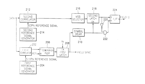
FIG. 4 is a detailed circuit view of the field
identification signal generating circuit 200 shown in FIG. 3.
Referring to FIG. 4, VSB data is applied from the matched
filter 110 of FIG. 3 to the first input of a first correlator
202. The second input of the first correlator 202 is
connected to the output of a first reference signal generator
204. The first input (A) of a comparator 206 is connected to
the output of the first correlator 202, the second input (B)
thereof is connected to a predetermined reference value (REF),
and the output thereof is connected to the input of a first
latch 208. The symbol clock frequency (fs), from the symbol
clock restorer 112 of FIG. 3, is applied to the enable input
(EN) of the first latch 208. The output of the first latch
208 is connected to the input of a symbol delay 210.
The VSB data is applied from the matched filter 110 to
the first input of a second correlator 212. The second input
of the second correlator 212 is connected to the output of a
second reference signal generator 214. The output of the
second correlator 212 is connected to the input of a most
signi~icant bit (MSB) selector 216.
CA 0222~37l l997-l2-l9
The input of a second latch 218 iS connected to the
output of the MSB selector 216. The enable input (EN) of the
second latch 218 iS connected to the output of the symbol
delay 210. The output of the second latch 218 iS connected to
both a set input (S) of a set-reset flip-flop (S-R F/F) 224
and to the input of an inverter 220. The first input of an
AND gate 222 iS connected to the output of the inverter 220,
the second input thereof is connected to the output of the
symbol delay 210, and the output thereof is connected to a
reset input (R) of the S-R F/F 224. A field identification
signal (FIELD ID) is output from the output (Q) of the S-R F/F
224. Here, the inverter 220 and the AND gate 222 can be
replaced by an exclusive OR gate. Also, in order to simplify
the hardware of the first and second correlators 202 and 212,
each the MSB selector can be provided before the first and
second correlators 202 and 212.
Operation of the circuit shown in FIG. 4 will now be
described. The VSB data as shown in FIG. 1 is input to the
first inputs of both the first and second correlators 202 and
212. The first reference signal generator 204 generates a
pseudo random number having a reference signal of 511 symbols
length (511PN reference signal). That is, the same signal as
the 511PN included in the field synchronous signal sequence as
shown in FIG. 2 iS generated. The second reference signal
2 5 generator 214 generates a pseudo random number having a
reference signal of 63 symbols length (63PN reference signal).
That is, the same signal as the 63PN included in the field
synchronous signal sequence as shown in FIG. 2 iS generated.
CA 0222~371 1997-12-19
The 511PN and 63PN reference signals, generated by the first
and second reference signal generators 204 and 214, are
applied to the second inputs of the first and second
correlators 202 and 212, respectively.
Accordingly, the second correlator 212 calculates a 63PN
correlation value by accumulating a value representing the
correlation between the VSB data and the 63PN reference
signal, in units of 63 symbols, thereby outputting three 63PN
correlation peak values with respect to 63PN in every field as
shown in FIG. 5A. Alternation of solid and dotted lines for
the middle of the three correlation peak values shown in FIG.
5A indicates that the polarity of the correlation peak value
is alternately inverted from positive to negative in field
units, or vice-versa. The above phenomenon occurs because, as
described above, the phase of the second 63PN, of the three
63PNs included in the field synchronous signal sequence, is
alternately inverted in every field according to the VSB frame
format.
Also, the first correlator 202 obtains a 511PN
correlation value by accumulating a value representing the
correlation between the VSB data and the 511PN reference
signal in units of 511 symbols, thereby outputting a
correlation peak value with respect to 511PN in every field as
shown in FIG. 5B. The peaks shown in FIGS. 5A and 5B are
generated only at the time when the 511PN and 63PN signals of
the field synchronous signal sequence occur, and are
represented as values being almost zero except in the field
synchronous signal. Here, in order to simplify the hardware,
CA 0222~371 1997-12-19
the first and second correlators 202 and 212 receive only a
sign bit of VSB data received, and can detect the 63PN and
511PN correlation values, respectively.
Meanwhile, the output of the first correlator 202 is
input to the first input (A) of the comparator 206. The
comparator 206 compares the output of the first correlator 202
with a reference value (REF) input through the second input
(B), and outputs a logic "high" signal only when the output of
the first correlator 202 is greater than or equal to the
reference value (REF). That is, when input data is a 511PN
synchronous signal sequence, it uses the fact that the
correlation value obtained by the first correlator 202 is at a
maxlmum .
The output signal of the comparator 206 is latched by the
first latch 208 according to a symbol clock frequency (fs),
and the output of the first latch 208 is output as a field
synchronous signal (FIELD SYNC) and simultaneously applied to
the symbol delay 210. In addition, when a very large noise,
ghost, interference, etc. is included in the transmitted
signal, the correlation between the 63PN signal and the 63PN
reference signal is small. However, since the 511PN
correlation value is about eight times greater than the 63PN
correlation value, a field synchronous signal is detected
using the 511PN correlation value. Here, strictly speaking,
the field synchronous signal output by the first latch 208 is
a field synchronous timing signal.
The symbol delay 210 delays by 126 symbols the 511PN
correlation value latched by the first latch 208 and outputs
CA 0222~371 1997-12-19
the delayed 511PN correlation value as shown in FIG. 5C. That
is, the 511PN correlation value of the waveform (FIG. 5C),
output by the symbol delay 210, coincides with the middle of
the three 63PN correlation values.
Meanwhile, the MSB selector 216 selects only the MSB of
the output of the second correlator 212, and outputs the
result to the second latch 218. That is because the present
invention requires only information on the polarity of the
three 63PN signals in the output of the second correlator 212
in order to generate a field identification signal by
detecting the polarity of the second of the three 63PN
signals. Here, the VSB data is 2's complement data.
The second latch 218 latches the MSB of the 63PN
correlation value output by the MSB selector 216, according to
the output signal of the symbol delay 210, and outputs only
the middle of the three 63PN correlation values which are
generated in every field, as shown in FIG. 5D. The output
signal of the second latch 218 is input to the inverter 220
and simultaneously to the set input (S) of the S-R F/F 224.
The output signal of the second latch 218, inverted by the
inverter 220, is input to the first input of the AND gate 222,
and the output signal of the symbol delay 210 is input to the
second input of the AND gate 222. A signal having a waveform
shown in FIG. 5E is output by the AND gate 222 and input to
the reset input (R) of the S-R F/F 224. Here, the waveform
shown in FIG. 5E has the form of the waveform of FIG. 5D, but
with the positive and negative parts exchanged. In the end,
the timing of the waveform of FIG. 5D agrees with when the
CA 0222~371 1997-12-19
second 63PN signal is positive, and the timing of the waveform
of FIG. 5E agrees with when the second 63PN signal is
negative.
The output signals (FIG. 5D and FIG. 5E) of the second
latch 218 and the AND gate 222, respectively, control the
setting and resetting of the S-R F/F 224. Accordingly, logic
"high" and "low" field identification signals (FIELD ID),
having the waveform shown in FIG. 5F, for identifying an odd
field and an even field, are alternately generated at the
output of the S-R F/F 224, in every field.
As described above, in a receiver for receiving a high-
definition signal, a field identifying signal for correctly
identifying an odd field and an even field is generated using
a 63PN signal whose phase is alternately inverted in every
field. An appropriate field identifying signal is provided to
a waveform equalizer or a channel decoder of the receiver,
thereby facilitating signal processing. Furthermore, the
structure of the present invention is very simple, so it is
very effective for hardware realization.