Note: Descriptions are shown in the official language in which they were submitted.
CA 0222~677 1997-12-22
Doc.No.18-17CA Patent
Multiple Parasitic Coupling to an Outer Antenna Patch Element from Inner
Path Elements
Field of the Invention
This invention relates to high-gain broadband antennas and more particularly to
5 an efficient, low profile patch antenna.
Background of the invention
It is highly desirable to produce a compact lightweight efficient low-profile high-
gain broadband antenna for use in wireless communications. Unfortunately, presently,
antennas encompassing all of these qualities are not available. Usually, antenna design
10 dictates that a trade off is necessary between size, bandwidth and efficiency. Recognition
of the trade off has resulted in several prior art design approaches for antennas.
A reflector antenna, commonly a parabolic reflector, uses a horn radiator to
illnmin~te its aperture. The shape of the reflector causes it to redirect energy fed to it by
the horn in a high gain directional beam. Unfortunately, a horn-fed reflector is inefficient
15 and bulky. Illumination of the reflector always results in either overspill or
underutilisation of available aperture. This inefficiency means that a larger reflector dish
than required is used to ensure underutilisation and thereby to prevent energy loss caused
by overspill. Typical efficiencies that can be achieved by a reflector antenna are 60%.
Overall size results from a boom supporting the horn and by the reflector dish.
Another approach to antenna design for communications uses an array of
microstrip patches or another form of printed radiator. Arrays of microstrip patches group
many low gain elements together, each fed so as to contribute to formation of a high gain
beam. Power is distributed to each of the elements via a feed network, which is the
primary source of inefficiency of the antenna. It is well known that large feed networks,
due to the line loss, significantly reduce antenna efficiency.
The above-described arrays are low-profile but suffer in efficiency due to the
heavy losses in the feed network. This increases the required array size for a given gain
CA 0222~677 1997-12-22
Doc.No.18-17CA Patent
requirement, but the nature of these feed networks is that feed losses become more
significant as array size increases. This makes achieving large efficient arrays very
difficult. Furthermore, the bandwidth of the above-described arrays is limited by the
bandwidth of the elements employed; if a narrowband element such as a simple
5 microstrip patch is used, the array bandwidth is no broader than the bandwidth of each
element.
Another approach currently employed is similar to the above-described array, butstacked microstrip patches are used instead of simple printed radiators. The stacked
microstrip patches alleviate bandwidth limitations inherent in the previously described
10 array antenna by providing a broad bandwidth element. Stacked patches are well known
in the art and comprise two or more patches stacked on top of each other. Each
successively higher patch is smaller than those below. Each smaller patch uses the one
beneath it as it's ground plane, and radiates around the patch above. This technique
broadens bandwidth, but does not increase gain, as the patches all have similar radiation
15 characteristics. Bandwidths achieved using this technique can reach 40%.
Arrays of quad-patch elements differ from the previously described arrays in that
an array element comprises a sub-array. The sub-array is fed by a single element below
each of the elements in the sub-array. For example, an array element consists of a first
patch which then parasitically couples to four patches disposed above the first patch with
20 a single corner of the first patch driving or feeding each patch of the four patches. This
reduces feed network complexity and feed network losses, because each group of four
radiating patches is fed by a single feed network line.
The use of the quad-patch antenna provides broad bandwidth, though to a lesser
extent than, for example, a stacked patch. A bandwidth of around 15% is achievable. The
25 feed loss problem is significantly reduced. The four patches are fed by directly coupling
to the first patch - the first patch couples parasitically to the upper four patches.
Unfortunately, this configuration is a compromise providing too little bandwidth and
insufficient efficiency when placed in large arrays. Also, it is incapable of expansion to a
CA 0222~677 1997-12-22
Doc.No.18-17CA Patent
multi-layer configuration because the feeding technique - one-corner-feeds-one-patch - is
limiting.
Object of the Invention
In an attempt to overcome these and other limitations of the prior art, it is an5 object of the invention to provide a low-profile, high-gain, broadband array antenna.
Summary of the Invention
In accordance with the invention, there is provided an array antenna comprising:a first radiator for coupling to a feed line;
10 a first array of radiators disposed so that each radiator within the first array of radiators is
in close proximity to the first radiator and spaced therefrom for parasitically coupling to
the first radiator;
a second array of radiators disposed so that each radiator within the second array of
radiators is in close proximity to a radiator in the first array of radiators and is spaced
15 therefrom for parasitically coupling to a radiator from the first array of radiators and
wherein some of the radiators in the second array of radiators is in close proximity to a
plurality of radiators from the first array of radiators for parasitically coupling to the
plurality of radiators from the first array of radiators.
20 Brief Description of the Drawings
An exemplary embodiment of the invention will now be discussed in conjunction with
the attached drawings in which:
Fig. 1 is a simplified oblique view of an array antenna designed by extension of quad-
25 patch radiator designs;Fig. 2 is a simplified diagram of a multi-layer array of patches to form a patch antenna
array designed by extension of the quad-patch antenna radiator designs;
Fig. 3 is a simplified diagram of an array antenna according to the invention in a "V"
configuration;
CA 0222~677 1997-12-22
Doc.No.18-17CA Patent
Fig. 4 is a simplified cross section of an array antenna according to the invention in a
"VVV" configuration;
Fig. 5 is a simplified oblique view of an array antenna according to the invention in the
"V" configuration and having 10 patches arranged in 4 layers;
5 Fig. 6a is a simplified schematic view of a microstrip patch array antenna in a "V"
configuration according to the invention comprising 5 patches on the outer most layer;
Fig. 6b is a simplified layer view of the microstrip patch array antenna of Fig. 6a;
Fig. 6c is a simplified cross sectional manufacturing view of layers employed in the
antenna of Fig. 6a;
10 Fig. 7a is a frequency response graph for the antenna of Fig. 6a;
Fig. 7b is a graph of a far field radiation pattern generated by the antenna of Fig. 6a;
Fig. 8a is a simplified schematic view of a microstrip patch array antenna in a "VVV"
configuration according to the invention comprising 12 patches on the outer most layer;
Fig. 8b is a simplified layer view of the microstrip patch array antenna of Fig. 8a;
15 Fig. 8c is a simplified cross sectional manufacturing view of layers employed in the
antenna of Fig. 8a;
Fig. 9a is a frequency response graph for the antenna of Fig. 8a;
Fig. 9b is a graph of a far field radiation pattern generated by the antenna of Fig. 8a;
Fig. 10 is a simplified layer view of a microstip patch array antenna in a "V"
20 configuration according to the invention comprising 12 patches on the outer most layer;
and,
Fig. 11 is a simplified cross sectional manufacturing view of layers employed in the
antennaofFig. 10.
Detailed description of the Invention
Referring to Figs. 1 and 2, a brief description of obvious extensions to the quad-
patch antenna of the prior art is presented. The quad-patch antenna uses one patch corner
to feed one patch. The logical extension to this is to continue using the same one corner
feeds one patch methodology, configurations of which are shown in Figs. 1 and 2.Neither of these configurations provides desired performance. In essence, these obvious
extensions are substantially unworkable for one reason or another. Patch overlap and
CA 0222~677 1997-12-22
Doc.No.18-17CA Patent
array irregularities or patch spacing are of significant concern and gain and bandwidth
requirements as desired are not achieved in an obvious fashion. The antenna array of Fig.
2 is also obviously limited in terms of gain, size and application.
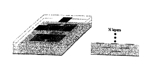
Referring to Fig. 3, a multi-layer array is provided wherein each patch, other than
5 those directly coupled to the feed or the feed network, is coupled parasitically. Multiple
parasitic coupling to an outer antenna patch element from an inner patch element results
in increased efficiency by elimin~ting all or a large portion of the feed network. In
general, the principle is similar to the quad-patch radiator described above; however, here
some patches are fed by more than one feed patch thereby overcoming limitations in the
10 embodiments of Figs. 1 and 2.
In the embodiment of Fig. 3, a single feed is used to feed a first patch. The first
patch is parasitically coupled to four patches, one patch of the four patches fed by each
corner of the first patch. Those four patches are parasitically coupled to S further patches.
Each of these further patches is fed by more than one patch of the four patches. The total
l S size of the array is dependent upon the number of layers and the number of patches fed.
In Fig. 3, three layers and one first patch result in an outer layer having S radiating
patches. This multi-layer structure is mounted on a single ground plane.
On each successive layer, the patches are designed with reduced size. This
provides increased bandwidth. Unfortunately, due to phase related issues, a V antenna is
20 limited to a gain of about 1 SdB unless phase related considerations are accounted for
during design and manufacture. For example, when spacing and dielectric materialbetween elements is chosen to ensure appropriate phase at each element in the outer layer
or, more preferably in each layer, gain can be increased significantly by increasing the
number of layers in the antenna array. This is discussed further with reference to Fig. 10.
Design of an antenna array having a "V" configuration is possible for e-plane
operation, h-plane operation or operation in both the e-plane and the h-plane. This
depends greatly on design criteria and desired operating modes.
CA 0222~677 1997-12-22
Doc. No. 18-17 CA Patent
Referring to Fig. 4a, another configuration - the "VVV" configuration - is shown.
In this configuration, only three layers are used for constructing the array antenna.
Patches on the centre layer of the three layers are parasitically coupled to patches on each
of the other two layers such that, with the exception of the patches adjacent the fed patch
5 (shown on the lower layer in Fig. 4a), each patch on the centre layer is fed from a patch
on the outer layer (shown as the top layer in Fig. 4a) and feeds another patch on the outer
layer. The result is an easily manufactured patch antenna having high gain, broad
bandwidth, and high efficiency.
Referring to Fig. 4b, an alternative design approach for implementing the "VVV"
10 configuration is shown which employs only two layers. The design approach results in
patch elements located so as to parasitically couple the fed patch to patches on another
layer. These patches are parasitically coupled to patches on a same layer as the fed patch.
By continuing the design to form an up-down parasitic coupling pattern, the antenna
array can be extended along each of two axes, one of which is shown in Fig. 4b.
In design of such an antenna, phase is easily maintained through accurate patch
spacing. Essentially, when patch spacing is substantially 360 degrees, phase of a radiated
signal from each patch is substantially the same. This is analogous to design and
implementation of a series feed which is well known in the art.
The "VVV" configuration has a narrower bandwidth than the "V" configuration
20 because the desired phase distribution can only be maintained over a narrower bandwidth.
Design of an antenna array having a "VVV" configuration is possible for e-plane,h-plane or both. This depends greatly on design criteria and desired operating modes.
Design criteria are well known in the art.
A multi-layer antenna configuration, based upon multiple parasitic coupling frominner patch elements to an outer antenna patch element, provides broadband performance
due to the multiple resonances of the structure. High gain with high efficiency is obtained
because a large aperture is fed without the use of transmission line feed networks. The
CA 0222~677 1997-12-22
Doc.No.18-17CA Patent
embodiments shown in Figs. 3 and 4 are both printed antennas and, therefore, are low-
profile and lightweight.
Referring to Fig. 5, a simplified cross sectional view of an array antenna
according to the invention is shown. Multiple parasitic coupling to an outer antenna patch
5 element from inner patch elements are used. Some patches are fed by 4, 3, 2, or 1 other
patches from another layer. Of course, 5 or more patches may feed a single patch in some
applications. In other words, two or more patch corners are used to feed another patch.
Design of another low-profile high gain broadband antenna having multiple parasitic
couplings in configurations as described herein, is unknown to the inventors.
Referring to Fig. 6a, an array antenna design using the "V" configuration and
having 5 patches on its outer layer is shown. Dimensions are shown for each patch.
Referring to Figs. 6b and 6c, layer related information is shown for the antenna of Fig.
6a. Using these three figures, a "V" configuration antenna according to the invention is
easily implemented. Simulated response of an antenna as shown in Figs. 6a, 6b, and 6c is
15 presented in Figs. 7a and 7b. As is evident from these response graphs, the antenna meets
desired objectives.
Referring to Fig. 8a, an array antenna design using the "VVV" configuration and
having 12 patches on its outer layer is shown. Dimensions are shown for each patch.
Referring to Figs. 8b and 8c, layer related information is shown for the antenna of Fig.
20 8a. Using these three figures, a "VVV" configuration antenna according to the invention
is easily implemented. Simulated response of an antenna as shown in Figs. 8a, 8b, and 8c
is presented in Figs. 9a and 9b. As is evident from these response graphs, the antenna
meets desired objectives.
Referring to Fig. 10, a "V" configuration antenna having 12 patches on its outer25 layer is shown. As described above, when such a design is used to achieve high gain
antenna arrays, phase is of concern. As shown in Fig. 11, Different dielectric materials
are used in the upper most dielectric layer in order to modify phase of the signals fed to
patches on the top layer. This results in a high gain "V" configuration antenna that
substantially m~int:~in.~ phase across all radiating patches in the outer layer. Of course, to
CA 0222~677 1997-12-22
Doc.No.18-17CA Patent
minimi7e discontinuities and facilitate phase shifting, it is preferable when constructing
large arrays that different dielectrics are used throughout ensuring proper phase at
substantially all of the patch radiators. .
The potential applications for medium to high gain planar arrays are numerous
5 including RADAR systems, terrestrial wireless systems, and satellite communications
systems.
Numerous other embodiments of the invention may be envisaged without
departing from the spirit or scope of the invention.