Note: Descriptions are shown in the official language in which they were submitted.
CA 02225681 1997-12-23
WO 97/01854 PCT/US96/10780
Barrier Layer for Ferroelectric Capacitor
Integrated on Silicon
Field of the Invention
The invention generally relates to ferroelectric and other high-dielectric
perovskite-based memories. In particular, the invention relates to a material
structure allowing ferroelectric material to be formed as crystalline material
over a
silicon substrate.
Back4round of the Invention
Most of the memory devices that are now commercially available are based
on silicon technology, which has enjoyed enormous commercial and technical
success because of its increasing device density and decreasing cost. One of
the
most popular memory devices is a dynamic random-access memory (dRAM) which,
in essence, is a capacitor usually composed of polysilicon electrodes
sandwiching a
silicon dioxide gap. The leakage current across the gap is small enough to
allow
charge to be stored on the cell for a few milliseconds without active
powering, after
which the cell is refreshed by reading its present value and, if a charged
state is
detected, restoring the original quantum of charge. For applications in which
periodic refreshing is operationally a problem, a static RAM (sRAM) is
available,
which in essence is a flip flop that can be switched between two stable
powered
states, but, if the power is removed, the memory state is lost. That is, both
dRAMs
and sRAMs are volatile. However, some applications require at least some
memory
be non-volatile so that the stored data is retained even if no power is
applied to the
memory cell over long periods. Read-only memory (ROM) has this capability but,
in
general, cannot be rewritten with new data. Various types of electrically
alterable
ROM (EAROM) have been developed, typically relying on charge injection into an
insulating layer, but their writing speed is usually very stow and requires
high
voltages.
-1-
CA 02225681 1997-12-23
WO 97/01854 PCT/LTS96/10780
As a result, significant development has occurred over the past few years in
ferroelectric memories which, of themselves, do not use a silicon-based
material for
the memory material but instead use as the storage medium a ferroelectric
material,
such as lead zirconium i:itanate (PZ T ). i he faiiosrvif y discuss~i~~ ~ wi+~
use PZT a~s the
prototypical ferroelectric, but the invention is equally applicable to many
other
ferroelectric materials.
The ferroelectric material is sandwiched between two electrodes to form a
capacitor. A ferroelectric is characterized by being switchable between two
states of
electrical polarization. Either of the two states is stable after power is
removed, and
the polarization state can be measured by measuring the polarity of charge the
ferroelectric induces on the capacitor plates. Therefore, ferroelectric
memories are
non-volatile and can be integrated to high densities similarly to silicon
dRAMs.
Often ferroelectric memory cells are directly integrated into gate electrodes
for
silicon electrodes, as disclosed by Lampe et al. In U.S. Patent 5,146,299.
However, commercially available ferroelectric memories have not been as
densely integrated into large arrays as desired. It is believed that many of
the
problems originate from the polycrystalline nature of ferroelectric material
grown
over a metallic electrode. The high quality of polycrystalline material is
difficult to
maintain for very small cells. Furthermore, the polycrystalline grain
boundaries
present failure modes for the thin ferroelectric material desired for dense
integration,
that is, a large number of memory cells on one chip. Inam and I recognized in
U.S.
Patent 5,155,658 that yttrium barium copper oxide (YBCO) could be epitaxially
formed over a crystalline substrate and crystalline ferroelectric lead
zirconate
titanate (PZT) epitaxially formed thereover and the YBCO would act as a bottom
electrode for the resultant ferroelectric memory cell. This structure was
modeled
after previous work disclosed by myself and Tarascon in U.S. Patent 5,168,240.
Although the above perovskite materials, e.g. YBCO and PZT, have been
shown to grow as single crystals on a crystalline perovskite substrate, it is
much
preferable if a silicon substrate can be used. Silicon wafers are widely
available
and inexpensive, and an integrated memory array requires support circuitry
best
-2-
CA 02225681 1997-12-23
WO 97/01854 PCT/L1S96/10780
implemented in silicon. Hence, the need exists to grow crystalline
ferroelectrics on
a silicon substrate. In the past this development have concentrated on the
optimum
' selection of a buffer layer to chemically isolate the underlying silicon
from the
ferroelectric and template layer thereover to initiate the crystallization and
formation
of the correct phase in the desired crystallographic orientation.
In U.S. Patent 5,270,298, I disclosed a structure in which the (100)-oriented
silicon substrate is overlaid with ytrria stabilized zirconia (YSZ) followed
by a
templating layer of an anisotropic perovskite, such as YBCO or bismuth
titanate
(B14TI3O~2, hereinafter BTO). Thereover is grown the multi-layer crystalline
perovskite device structure. As an example, the ferroelectric capacitor is a
YBCO/PZT/YBCO structure which relies upon the metallic properties at room
temperature of the prototypical perovskite superconductor YBCO. The YSZ layer
acts not only as a buffer layer but also as a barrier to prevent the diffusion
of
chemical species from the layer above into the silicon substrate, which could
further
migrate to degrade semiconductor devices formed on the silicon substrate. The
bottom YBCO electrode, which grows in a c-axis orientation and with very high
crystalline qualify, serves both as an electrical contact and as a structural
template
for the subsequent growth of the cubic PZT layer.
However, YBCO suffers from the disadvantage that, to be grown with a c-axis
orientation, the substrate heater temperature needs to be close to
800°C although
the substrate surface temperature is about 50°C lower. Such
temperatures are not
completely compatible with the Si-CMOS processing desired for the support
circuitry
of the integrated fen'oelectric memory circuit. Furthermore, the use of
layered,
anisotropic perovskites, such as YBCO, for electrodes or other elements causes
problems that are best avoided.
The problems with YBCO electrodes can be avoided by the use of electrodes
~ of cubic metal oxides, which are isotropic and which grow with high
crystalline
quality at much lower temperatures. One such oxide is t_aSrCo03 (t_SCO,
actually
' approximately La~_xSrXCo03, where x is between 0.15 and 0.85, preferably
about
0.5), which grows with almost singly crystalline quality in the temperature
range of
-3-
CA 02225681 1997-12-23
WO 97/01854 PCT/US96/10780
550-650°C. Other examples are LaCr03, SrRu03, and related metallic
perovskites.
However, these cubic metallic oxide materials grown directly on a YSZ-buffered
silicon substrate with the desired crystallographic orientation, and
consequently the
subsequent'ry grown ferroeiectric PZT have poor crystaiiographic properties.
However, in U.S. Patent 5,270, 298, we describe the highly crystalline growth
of LSCO on YSZ-buffered silicon by the use of an intermediate, thin (20 to
40nm)
layered perovskite, especially BTO. When a c-axis oriented
crystallographically
templating layer is grown at a suitable temperature (in the case of BTO in the
temperature range of 600-690°C and optimally at about 640°C),
the templating layer
prefers to grow with its c-axis normal to the silicon substrate. The
preference in
crystallographic growth direction arises from the anisotropic crystal
structure of
these layered perovskites and the consequent anisotropy of the surface
energies of
different crystallographic facets. In this case, the lowest-energy surtace is
the a-b
plane, that is, the surface that is normal to the c-axis and has an
approximately
square surface lattice spacing,
The a-b plane of the layered perovskite templating materials have in-plane
lattice dimensions and crystal chemistry, that is, metal-oxygen bonding, that
are
almost identical to those of the cubic perovskites. Consequently, when the
cubic
perovskite such as LSCO or the anisotropic ferroelectric perovskite PZT is
grown on
top of the templating layer, it grows in the desired crystallographic phase
and
orientation, the perovskite phase with typically the (001 )-direction being
normal to
the surface. The cubic perovskite grown in this fashion usually manifests
excellent
crystalline quality, as evidenced by x-ray diffraction and transmission
electron
microscopy, anct;~nore importantly, exhibit very desirable ferroelectric
properties,
probably due to the chemical templating that occurs in crystallographical
templating
of similar metal-oxide materials. This templating approach is quite general
and
hence can be used to grow a variety of cubic perovskite oxides or other more
complex perovskites on top of typically YSZ-buffered silicon wafers, thus
marrying
two very dissimilar types of materials and leading to a vast range of
potential
applications.
CA 02225681 1997-12-23
WO 97/01854 PCT/IJS96/10780
Rather than following Lampe et al. and connecting the ferroelectric memory
cell to the gate of a transistor, a preferred approach in making an integrated
ferroelectric memory element involves selectively delineating a ferroelectric
capacitor that is electri~;;y connected to the drain or source of the silicon
pass-gate
' S transistor. Accordingly, the interface between the silicon and the
ferroelectric stack
must remain conductive.
In operation, an electrical signal applied to the gate of the pass-gate
transistor determines whether the ferroelectric capacitor is connected to the
word
line for reading or writing or is isolated from it. Pass-gate transistors
typically are
configured as CMOS transistors with SiOz as the gate dielectric. Therefore, it
is
preferable that the ferroelectric deposition be carried out under conditions
compatible with prior silicon CMOS processing. Even better, the ferroelectric
memory cell should be grown in or on an Si02 layer already formed on the
silicon
wafer for part of the CMOS fabrication process. However, experience has
generally
shown that direct growth of the cubic perovskite, for example LSCO on Si02-
coated
silicon, produces a capacitor structure with poor ferroelectric properties.
I have however shown in U.S. Patent 5,248,564 that a templating layer of
BTO grown on SiOz under the correct growth conditions allows a layer of highly
oriented LSCO to be grown thereover. The LSCO acts both as an electrode and a
crystallographically templating substrate layer for an upper ferroelectric
layer of PZT
templated to a c-axis orientation. Its thickness should be sufficient that the
overlayers do not contact the SiO~/Si substrate. The BTO layer is a thin
templating
layer of a layered perovskite which has a,b lattice parameters that are
closely
matched to those-of the overgrown cubic perovskite LSCO.
There results a c-axis oriented LSCO/PZT/LSCO ferroelectric capacitor
grown on an Si02-buffered silicon wafer. Although these capacitive structures
show
quite desirable ferroelectric properties, the electrical conductivity of the
LSCO
electrodes is lower than desirable for an integrated circuit memory array and
lower
. ' than that obtainable from a more conductive material, such as metallic
platinum,
which would need to be placed at the bottom of the later grown crystalline
-5-
CA 02225681 2001-02-16
ferroelectric memory stack.
I have described in U.S. Patent No. 5,479,317, issued December 26, 1995,
that a very highly oriented thin film of platinum can be grown on the surface
of a
substrate such as Si02 covered Si, even though the surface is amorphous. For
example, as shown in cross section in FIG. 1, an Si02 layer 10 is grown over a
Si
substrate 12, which is understood to possibly include different layers defined
vertically by doping and perhaps also laterally defined for a silicon
transistor. A
template layer 14 of BTO grown to a thickness of 30 to 50nm at a temperature
range of 640 to 680°C forms with a c-axis orientation. Then, when a
platinum thin
film 16 is grown on this surface at a growth temperature of 580 to
640°C, it is
grown with a very strong (001 )-orientation. The oriented platinum film 16
allows
after grown-layers, such as a ferroelectric stack including to cubic, metal-
oxide
layers 18 and 20 of LSCO sandwiching a ferroelectric PZT layer 22, to be
epitaxially deposited with a strongly crystalline or at least highly oriented
structure.
Thereby, a crystalline ferroelectric memory can be formed. The ferroelectric
material is quite general. It may be PZT or other cationically substituted
derivatives
such as lead lanthanum zirconium titanate (PLZT) or lead niobium zirconium
titanate (PNZT) or similar materials in which substitutions of donor dopants
such as
La, Nb, or others occur at the Pb site. In PZT, the ratio of zirconium and
titanium
can be greatly varied. I have disclosed yet other ferroelectric materials in
U.S.
Patent No. 5,519,587, issued May 21, 1996.
Although the crystallographically templating approach provides highly
oriented ferroelectric capacitor stacks with excellent ferroelectric
reliability
characteristics, the bismuth titanate template layer requires an additional
deposition step and an additional etching step in the formation of the memory
element. It would be preferable to grow the ferroelectric material on a
silicon wafer
without the intervening layered-perovskite template layer. Furthermore, a
metallic
layer beneath the ferroelectric layer would be more preferable even though
past
experience has shown that PZT grown on platinum leads to poor ferroelectric
properties, notably poor fatigue characteristics. Finally, CMOS pass-gate
-6-
CA 02225681 1997-12-23
WO 97/01854 , PCT/LTS96/10780
transistors require a silicon oxide layer over the silicon wafer. It would be
preferable
to grow the ferroelectric stack on a SiO~/Si wafer with an intervening Pt
layer to
- reduce sheet resistance, but without the necessity of a template layer. The
structure ir~ the afcre~era ;~ ~ed-Patent App;ica;io~ , ''2~, as illus.r ated
in cross
' S section in FIG. 2, is~ similar to that of FIG. 1, but there is no BTO
crystallographically
templating layer but a titanium layer 24 underlies the Pt layer 16 on top of
the Si02
layer 10. While this structure works for ferroelectric stacks over an silicon
dioxide
layer, a similar stack formed over silicon requires that the silicon-to-metal
oxide
interface not be further oxidized.
The above described growth processes, while useful for memory integration
on the order of 1 MB, suffer disadvantages for higher density architectures in
which it
is much preferable that the capacitor structure be directly integrated with
the silicon
circuits and be in direct electrical contact with the Si-based CMOS part of
the wafer.
The contact to the silicon wafer is typically made through a polysilicon plug
that is
deposited on the silicon wafer without any interfacial Si02 layer. It is
imperative that
during deposition of the ferroelectric no oxygen diffuse downwardly to the
polysilicon
and oxidize it into insulating Si02. However, contacting the polysilicon plug
to the
ferroelectric capacitor stack is quite difficult since the ferroelectric
stack, such as
LSCO/PZT/LSCO, is grown under highly oxidizing ambients at elevated
temperatures in the range of 550-700°C. Oxygen is thus readily
available and at
high. temperatures so that it easily diffuses to the pofysilicon plug with
which it forms
a surface layer of Si02, thereby breaking the electrical contact between the
polysilicon and the ferroelectric stack. Platinum is a preferred metallic
contact layer
for ferroelectric~ Although oxygen does not significant react with Pt, it
readily
diffuses through the Pt to react with underlying layers.
As a result, a barrier layer needs to be inserted between the polysilicon plug
and the bottom electrode of the ferroelectric stack. Barrier layers such as
TiN are
well known but are not viable in this situation because they too are oxidized
under
the processing conditions used to fabricate the ferroelectric stack.
-7-
CA 02225681 1997-12-23
WO 97/01854 PCT/L1S96/10780
Summary of the Invention
The invention can be summarized as a ferroelectric capacitive cell in which a
conductive perovskite layer, especially a cubic perovskite layer, is formed
over the
metal electrode and serves as a chemical template for the perovskite
ferroelectric
layer. A composite diffusion barrier is used to isolate the underlying
silicon, usually
a polysilicon plug, from the harshly oxidizing environment prevalent during
deposition of the perovskite ferroelectric stack, for example, of
LSCOIPZT/LSCO. In
a first embodiment, the diffusion barrier may be a refractory metal layer
beneath a
platinum layer. The oxygen diffuses through the platinum but reacts with the
refractory metal to form balls of refractory oxide within a platinum matrix.
In a
second embodiment, an intermetallic layer prevents oxygen diffusion to the
silicon.
In a third embodiment, Ru and SrRu03 and similar material combinations acts as
an
electrode and oxidation barrier.
Brief Description of the Drawings
FIGS. 1 and 2 are cross-sectional views of a ferroelectric structure related
to
the invention and utilizing perovskite templating layers above a metal layer.
FIG. 3 is a cross-sectional view of a ferroelectric cell utilizing the barrier
layer
of the invention.
FIG. 4 is a cross-sectional view of a first embodiment of the invention
utilizing a cubic perovskite layer above a metal layer, wherein the
illustrated
structure does not account for oxidation produced in formation of the upper
layers.
FIG. 5 is a cross-sectional view of the embodiment of FIG. 4 showing the
effect of oxidation on the metal layers.
FIG. fi is a cross-sectional view of a second embodiment of the invention
utilizing an intermetallic alloy as the oxygen-diffusion ban-ier.
FIG. 7 is a cross-sectional view of third embodiment of the invention
utilizing
a strontium metal layer and a conductive strontium oxide layer.
CA 02225681 1997-12-23
WO 97/01854 PCT/US96/10780
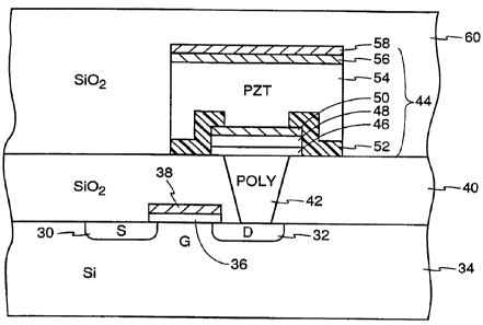
Detailed Description of the Preferred Embodiments
A general embodiment of the invention is illustrated in cross section in FIG.
3.
A source 30 and a drain 32 are formed in a silicon wafer 34. A gate insulator
layer
36 of Si02 and a metal contact and interconnect layer 38 are formed over the
gate
region. A field oxide 40 is deposited thereover. An area for a polysilicon
plug 42 is
etched through the field oxide 40 overlying the drain 32 and the plug 42 is
deposited
therein, and thereover is formed a ferroelectric stack 44. The structure of
FIG. 3
does not illustrate the contact to the source 30 and the gate, which may their
own
polysilicon plug with a metal contact thereover.
The dielectric stack 44, in this general embodiment, includes an electrically
conductive barrier Payer 46, a metallic layer 48, and a bottom conductive
metal oxide
electrode 50. The stack 44 is patterned and etched, and thereover is formed an
inter-dielectric layer 52 of Si02 or Ti02 conformally deposited over the lower
part of
the stack 44. Thereover is deposited a ferroelectric layer 54, a top electrode
56,
and a top metallization 58. These features are patterned and etched, and
thereover
is deposited another Si021ayer 60. The contact to the metallization is not
explicitly
shown. This illustration does not show contacts to the gate and drain, which
may be
similar or otherwise formed.
The barrier layer 46 of the invention prevents oxygen from the oxygen-rich
templating layer 48 and other overlying layers, typically formed of an oxide
metal,
from diffusing therethrough and oxidizing the top surface region of the
polysilicon
plug 42 into insulating silicon dioxide. Especially, the oxidizing atmospheres
used
to grow perovskite overiayers, preferably in the elevated temperature range of
500-650°C, strongly oxidize unprotected underlayers by the high-
temperature
diffusion of oxygen through typical overlayers.
In a first specific embodiment of the invention, illustrated in cross section
in
FIG. 4, a ferroelectric stack 70 includes a conventional base barrier layer 72
of TiN
deposited over the polysilicon plug 42, and over the TiN barrier layer 72 is
deposited an oxygen-diffusion ban-ier comprising a lower conductive metal
layer 74,
a refractory metal layer 76, and an upper metal layer 78. Preferably, the
conductive
_g_
i
CA 02225681 1997-12-23
WO 97/01854 PCT/US96/10780
metal layers 74 and 78 are composed of a conductive metal such as a noble
metal,
preferably platinum, and the refractory metal layer 76 is composed of Ti, Mo,
W, or
Ta. Thereover are formed a lower, conductive cubic perovskite layer 80, e.g.
of
LSCO, a PZT ferroelectric layer 82, and an upper, conductive cubic perovskite
layer
84. The lower, cubic perovskite layer 80 acts as a chemical template for the
formation of a c-axis oriented layered perovskite ferroelectric layer 82. The
LSCO
provides a metal that is octahedrally bonded with oxygen, which is chemically
compatible with the over-grown oxide PZT. The upper electrode layer 84, e.g.
of
LSCO is grown over the PZT layer 82 and an upper Pt layer 86 contacts the
upper
LSCO layer 84 and provides a metallization. The drain 32 is contacted by
separate
means, such as a polysilicon plug parallel to the source plug 42 with an
overlying
metal layer.
The refractory metals used in this invention are known getterers of oxygen.
When exposed to oxidizing ambients at elevated temperatures in the range of
550-650°C, such as are preferred for the growth of the LSCO and PZT
layers 80,
82, and 84, oxygen diffuses through the noble metal layer 78 and oxidizes the
refractory metal layer 76. As illustrated in cross section in FIG. 5, the
metal oxide
balls up and forms islands 90 in a platinum matrix layer 92. Thereafter, an
electrical
lead 94 is connected to the upper electrode layer 86, and the oxygen being
bound
up in the islands 90 will not prevent electrical contact through the Pt matrix
92.
Depending upon the type of metal that is used in the refractory layer 76,
these metal
oxide islands 90 can be either conducting, semiconducting, or insulating.
Examples
of other refractory metals usable in layer 76 are Ta and Mo.
This embodiment is related to what I have described in the aforementioned
U.S. Patent Application '728, namely an Si02-buffered silicon substrate
overlaid with
a hybrid stack of Ti followed by Pt, over which is deposited the LSCO/PZT/LSCO
ferroelectric cell. However, the two differ significantly. In the '728
application, an '
Si02 layer lies between the silicon substrate and the TilPt hybrid layer. The
Si02 is
highly insulating so diffusion of oxygen toward the substrate or oxidation of
Ti are
not critical problems. Indeed, the geometry of the patent application has both
-10-
CA 02225681 1997-12-23
WO 97/01854 PCT/US96/10780
contacts on the front side so that at the bottom only the LSrO electrode layer
need
conduct and the conductivities of the Pt and Ti layers are not critical. In
contrast, in
the embodiment of FIG. 5, the TiN layer 72 is conductive and the polysilicon
plug 42
must be protected against oxidation less it turn insulating and prevent
contacting
from the back side: Thus, the Pt and Ti layers 74, 76, and 78 are arranged
with a
double Pt structure sandwiching the oxidizable Ti to allow conductance around
the
balled-up TiOX.
A common theme exists between the two structures, namely, that
conventional crystallographic templates are not necessary for high quality
ferroelectric cell but chemical templates will suffice. A crystallographically
templating layer of BTO provides highly oriented crystallographic growth in
the
c-direction and also provides chemical consistency between the perovskite BTO
and
the after grown perovskite PZT or other ferroelectric layer. A templating
layer of
LSCO may afford some orientational templating, particularly when it is grown
over a
partially oriented Pt layer. However, the thermodynamics are not as strong as
for
the layered BTO. Instead, LSCO's principal contribution seems to be a
chemically
templating effect. The metal oxides such as PZT can grow in many different
phases, e.g., perovskite, pyrochlore, and rutile. Only the perovskite phase
demonstrates the desired ferroelectric effect. If the underlying layer,
however, is
formed of another perovskite material, such as LSCO, having the same
octahedral
bonding of oxygens around the metal atoms, the after-grown layer is much more
likely to form a high-quality perovskite layer without large intergranular
spaces
which promote various failures mechanisms. Although LSCO may well not cause
strong orientational templating of the PZT layer, the resultant PZT still has
sufr'icient
uniformity to avoid the fatigue problems which plague PZT grown on Pt without
further attempts to improve the crystallography.
If the refractory metal layer 36 is replaced by a Group VIII intermetallic
layer
of Ru, Ir, or Os, the oxide produced by oxidation is conductive and the layer
48 of
the intermetallic oxide may be fairly homogeneous after oxidation.
In a second embodiment of the invention, illustrated in cross section in
-11-
CA 02225681 1997-12-23
WO 97/01854 PCT/US96/10780
FIG. 6, a dielectric stack 100 includes a thin layer 102 of an oxidation-
resistant
binary intermetallic alloy, such as NiAI, NiTi, NiMn, or NiFe, deposited over
the
polysilicon plug 28. A platinum lower electrode 104 is grown over the
intermetallic
alloy layer 102, and the LSCO/PZTiLSCO stack 80, 82, and 84 is grown
thereover.
The intermetallic alloy 102, when grown at stoichiometric composition, is well
known
to be a very conductive metal and resistant to oxidation. Importantly, it acts
as a
barrier layer to the diffusion of oxygen during the high-temperature growth of
the
perovskites LSCO 80 and 84 and PZT 82. The intermetallic alloy 102 can have
the
general composition of approximately AB or A3B, where A can be Ni or Co and B
can be AI, Ti, Mg, Cr, or Fe.
A third embodiment of the invention, illustrated in cross section in FIG. 5,
employs a structure known to be effective in the integration of materials with
high
dielectric constants on a polysi(icbn plug. A dielectric stack 110 includes at
its
bottom a thin layer 112 of Ru deposited over the polysilicon plug 42 and which
acts
as an oxidation barrier. A thin layer 114 of SrRu03 or more generally
SrXRu2_X03,
where x is preferably about unity, so as to yield a stoichiometric layer, but
may have
values 0.9<x<1.1, is deposited over the Ru layer 112, it also acts as an
oxygen-
diffusion barrier and importantly forms in a perovskite structure to promote
chemical
templating for an overgrown perovskite layer 80, of, for example, LSCO. Both
layers
112 and 114 may be deposited by evaporation or sputtering. Ruthenium is a
conductive metal but its oxide forms a rutile, which does not provide the
required
templating. Strontium ruthenate on the other hand is a reasonably conducting
perovskite oxide. Whatever oxygen diffuses through the SrRu03 layer 62 will
form
RuOX in the Ru layer 112. This oxide RuOX is very highly conducting.
Furthermore,
the SrRu03 layer, being a perovskite structure oxide, helps in the nucleation
of the
desired perovskite structure in the LSCO/PZT/LSCO ferroelectric stack 110.
Alternatively, the metal/metal-oxide heterostructure may be formed of Ir and
SrXlr2_
X03. The metal layer of Ir and a metal oxide layer of Srlr03 have similar
properties to
the con-esponding Ru layers. The iridium layer is metallic and conductive, and
the
perovskite Srlr03 layer is adequately conductive.
-12-
CA 02225681 1997-12-23
WO 97/01854 PCT/US96/10780
Although the above embodiments have described ferroelectric memories, the
invention is equally applicable to memories and other semiconductor structures
in
which a perovskite layer forms a high-dielectric layer, e.g., in high-
performance
d RAMs.
The invention thus provides an oxidation barrier layer which allows an oxide-
based ferroelectric stack or other perovskite structure to be integrated with
a silicon
substrate.
-13-