Note: Descriptions are shown in the official language in which they were submitted.
rlttV VvvJV~ p~JC~VVy.tl.y
CA 02225930 1997-12-29
METHOD AND APPARATUS FOR MONOLITHIC'OPTOELECTRONIC INTEGRATED
CIRCUIT USING SELECTIVE EPITAXY
Field of the Invention
The field of the present invention relates generally to
photodetectors, and more particularly to photodetector diodes
included in integrated circuit form..
Background of the Invention
Photodetectors are comprised of a diode that permits an
amount of current to flow through it that is proportional to the
intensity of light with which it is illuminated and a readout
circuit for producing a voltage corresponding to the current
flowing through the diode and hence also corresponding to the
intensity of the light. Diodes using InGaAs are superior to
those using Gi, HgCdTe,PtSi or InSb for certain applications
because of their higher sensitivity, faster operation and the
fact. that they function well at room temperature.
If an InGaAs diode were epitaxially grown on the Si
substrate on which the readout circuitry is preferably formed,
the lattice mismatch would have so many dislocations as to cause
sufficient leakage current to seriously degrade diode
performance. For this reason a hybrid structure has been used
for several years wherein the diode is separate from the
substrate and coupled to its readout circuit thereon by wire or
Indium bump bonds. Unfortunately, however, such connections are
susceptible to vibration failure in a space launch and are
plagued by parasitic capacitance and inductance that lower their
reliability and decrease their bandwidth. Furthermore,
extensive packaging efforts are required in order to form an
array of such detectors.
3o As reported in ~Tourna.l Applied Physics (Vol. 65(6),
pg.2220-2237, 1989), E. A. Fitzgerald et a1 have selectively
grown Ina.~,Gao.~As on GaAs substrates with very few dislocations
1
i~W062696/S~S2007._PCT CA 02225930 1997-12-29
by canfining the epitaxial grawth to a location that is squares
or circular having an area of (100x100)um2 or less_
Zt is also known that if a desired epitaxial layer has a
lattice that is severely mismatched with the lattice of a
substrate on which it is epitaxially grown as to severely limit
the operation of a device of which it is a part. In such a
case, the desired epitaxial layer can be compositionally graded
to the substrate via successive epitaxial layers in which the
ratio of the elements respectively changes from that of the
desired composition to a composition having far less lattice
mismatch with the substrate.
Suaunary of the Invention
_ In accordance with this invention, a photodiode using
ZnGaAs is selectively epitaxially grown on an area of a Si
substrate that is less than 500~Cm2. The desired ratio of In to
Ga for the purpose of forming a light absorption layer of a p-n
ZnGaAs diode junction has a lattice constant so high as to form
a significant lattice mismatch with Si. Therefore, even if it
were grown directly onto a Si substrate within the limited area
referred. to above, the performance of the diode would be
severely impaired by the resulting leakage current. By making
the absorption layer having the desired ratio of In to Ga the
last of a stack of epitaxially grown InGaAs layers in which the
ratio of In tn Ga decreases as the substrate is approached, the
lattice mismatch with the substrate is reduced so that the
amount of leakage current is further reduced to a highly
acceptable low value.
In forming the p-n, junction, of course, the InGaAs material
on one side of the junction is doped so as to be of one
conductivity type, and the InGa~s material on the other side of
the junction is doped to be of the opposite conductivity type.
The material on the same side of the junction as the substrate
has the same type of conductivity as the substrate.
2
KW062696/8492001.PCT CA 02225930 1997-12-29
Although the stac3c of epitaxial layers could be grown on
the surface of the substrate, still further reduction in leakage
current is achieved by growing at least a portion of it in a
"well" or "trough" that has been etched in the substrate and
its cavering layer of Si02. Although. the entire stac3c could be
grown in the substrate, it is preferable that the p-n junction
formed in the stack be at the surface of the Si substrate in
which event InGaAs material having one conductivity type would
be above the surface and in contact with the Si02 and the InGaAs
material of the other conductivity type would be in contact with
the Si. of the substrate.
Readout circuit elements for the photodetector just
described are formed by CMOS processing in the surface of the
substrate, and the insulating layer of Si02 is formed on the
_ 15 surface surrounding the well. Connections between the
photodiode and the readout circuit elements are readily formed
on the Si.02 layer and matte contact with appropriate elements by
extending through the Si02 layer.
In a preferred monolithic structure, the photodiode is
formed in the well in one surface of the substrate as described,
a conductive layer is formed on the other surface, and diode
current flows vertically between the surfacas.
In a less preferred structure, the photodiode is on top of
a mesa and ohmic contacts. at different points on the p-n
junction are such as to form a "lateral" p-i-n diode between
them so that the current flow is parallel to the surfaces of the
substrate. Furthermore, the photodetector of this invention
is so structured as to make it.a simple matter to incorporate
a filter for selection of the bandwidth of light whose intensity
_ 30 is to be measured. In particular, it is. easy to combine the
photodetector with a resonant optical filter by providing layers
on tap of the photodetector serving as a partial mirror, a fully
reflecting layer on the opposite side of the substrate and
making the thickness of the substrate such that the. distance
between the two mirrors is .one half the wavelength of the light
of interest. __ _
3
RW062696/84~2001_PCT CA 02225930 1997-12-29
Manufacture of a monolithic photodetector such as described
above in accordance with another aspect of the invention
involves more steps than can be identified in this summary but
in general the readout circuit elements are formed in the
substrate, the well is etched and the layers of the stac3c. are
epitaxially grown in the well before metallizing to form the
circuit interconnections.
Brief Description of the Drawings
Various embodiments of the present invention are shown and
described herein with reference to the drawings, in which Like
items are identified by the same reference designation, wherein:
Fig. lA is a schematic of a circuit of a monolithic
photodetector;
Fig. 1B is a timing diagram for the circuit of Fig. lA;
Fig. 2A is an isometric view of the locations of readout
circuits and photodiodes of an array in which current flows
parallel to the substrate;
Fig. 2B is an isometric view of the locations of readout
circuits and photodiodes in which current flows through to the
substrate;
Fig. 3 is a cross sectional view of a monolithic
photodetector of this invention in which a mesa structure is
used and an optical resonant filter is provided;
Fig. 4 is a plot of lattice constant, energy band gap and
wavelength for different materials.
Fig. 5A is a cross sectional view of the preferred
photodiode structure showing its coupling to elements of a
readout circuit;
Fig. 5B is a cross sectional view of a slightly different
construction of the photodiode of Fig. 5A;
Figs. 6A, 6B, 6C, 6D and 6E are cross sectional views
illustrating successive steps in the fabrication of a preferred
specie of a photodiode of this invention; and
4
~~i,vu~o~a~ o~zwvv~..~~A 02225930 1997-12-29
Fig. 7 shows a curve for the forward-reverse I V
characteristic of a 500~m diameter InGaAs detector selectively
grown over silicon, in accardance with one aspect of the
invention (the x-axis is in Volts and the y-axis is in mA)..
Detailed Descriution of the Invention
In the schematic diagram of a photodetector shown in Fig.
1A light indicated at 2 illuminates a photodiode 4 so as to
change its conductivity and thus alter the voltage supplied to
a readout circuit 6 at the inverting input of an operational
amplifier 8. This invention does not involve the readout
circuit per se but merely requires that some readout circuit be
incorporated in the monolithic structure. The particular
readout.circuit shown by way of example is comprised of the
operational amplifier 8 connected as an integrator with a
capacitor 10 connected between its output and its inverting
input and a capacitor 12 connected between its output and a
noninverting input of an operational amplifier 14. The output
of the amplifier 14 is directly connected to its inverting input
so that it operates as a buffer. A switch S1 is connected in
parallel with the capacitor 10, a switch SZ is connected between
the noninverting input of the amplifier 14 and ground and a
switch S3 is connected to the output of the amplifier 14. The
switches S1, S2 and S3 operate in the sequence illustrated in Fig
1B so that the current supplied by the photodiode 4 is
integrated over a given period, thereby providing a voltage
indicating the intensity of the light 2.
In accordance with this invention, the photodiode 4 is
formed by selective epitaxial layers of InGaAs that are grown
on the same substrate in which. the circuit elements of a readout
circuit are formed. Fig. 2A is an isometric view of an array
of' photodetectors in which the photodiodes are located at the
circles 4~ and the readout circuits are located at the
rectangles 6i on a silicon substrate 16. In order to conserve
5
tSW062~96/Fi~~~uu.a..P~TT CA 02225930 1997-12-29
space, the readout circuits 6; could be formed around the
photodiodes 41.
Fig 2B is the same as Fig_ 2A except for the addition of
a conductive layer 18 on the surface of the substrate 16 that
is opposite to the surface bearing the photodiodes 41 and the
readout circuits 6i. As will be explained, the purpose of the
conductive layer 18 may be to act as a reflector of a resonant
optical filter and/or as an electrode of a photodiode 4i in
which current flows vertically from one surface of the substrata
16 to the other.
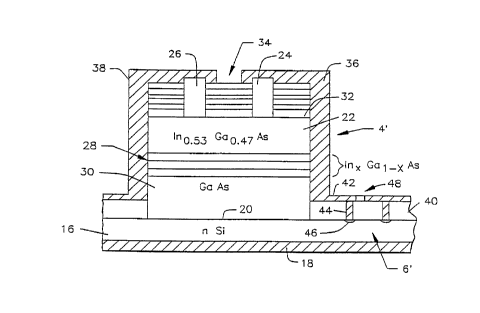
Fig. 3 is a cross sectional view 3, 3 of Fig. 2B in which
the photodiode 41 is formed on a mesa structure that is
selectively epitaxially grown onto a surface 20 of the substrate
16. Only the connection of the photodiode 41 to the input of
_ 15 the readout circuit 61 is shown, but it is understood that the
elements of the readout circuit would be formed in the surface
by CMOS techniques.
In particular, the photodiode 4I is comprised of an
absorption layer 22 of In4~Gao.4~As that provides more carriers as
20 the intensity of the light with which it is illuminated
increases. An ohmic electrode 24 made of. AuGe(n) is in
electrical contact with one point on the layer 22, and an ohmic
electrode 26 made of AuZn(pt) is in electrical contact with the
layer 22 so as to form a p-i-n diode between them. Thus as the
intensity of the illumination of the layer 22 increases, the
current flowing between the electrodes 26 and 24 increases.
If, however, the layer 22 were grown directly on the
surface 20 of the substrate 16, which, in this example, is made
of n-Si, the difference in the lattice constants would be about
10% so as to produce a large number of dislocations and hence -
a large leakage current. Therefore, in accordance with one
aspect _of this invention, the layer 22 is selectively
epitaxially grown on a stac3c 28 of selectively epitaxially grown
layers of n InzGal_,~s in which the value of x increases for
subsequently higher layers in the stack. A selectively grown
. _ buffer layer 30 , of GaAs is between the stack 28 and the surface
6
KW062696/8492001.PCT CA 02225930 1997-12-29
20 of the substrate 16.. The difference in the lattice constants
between adjacent ones of the layer 30, the layers of the stack
28 and the layer 22 is much smaller than 10% so as to reduce the
number of dislocations and the leakage current.
An important aspect of this invention is the still further
reduction in leakage current by making the cross sectional area
of the layer 30, the stack 28 and the layer 22 less than 500
,~m2. In this example, all layers have the same area. Also,
as indicated the ratio of In to Ga is varied to change the
lattice, while the relative amount of As is constant_
In this particular embodiment of the invention, a cap layer
32 of p Alo.~InaszAs is selectively epitaxially grown on top of
the diode layer 22, that has a higher band gap than the layer
22 so as to limit the surface leakage currents. Lower band gap
surfaces produce higher leakage currents which are not
desirable. Although an optical filter per se is not part of
this invention, the photodiode of the invention is adapted for
use with any kind of filter and especially adapted for
combination with a resonant optical filter. A partially
reflective mirror 34 is comprised of alternate layers of Si3N4
and Si02 that are formed on the layer 32, and a fully reflective
mirror is comprised of the coating 18 on the bottom surface of
the substrate 16 by, for example, making it of Au.
The operation of an optical resonant filter is well known
so suffice it to say that if the distance between the partially
reflective mirror 34 and the fully reflective mirror 18 is one
half the wavelength of the light whose intensity is being
measured, the light reflected by the mirror 18 will arrive at
the mirror 34 in phase with light from the source being measured
so as to increase the amount of light passing through the
photodiode absorption layer 22. This permits the thickness of
the layer 22 to be reduced_thereby further decreasing leakage
current.
Connection of the electrodes 24 and 26 of the photodiode
41 to the readout circuitry 6i is via metallized paths 36 and 38
respectively. An insulating layer 40 of Sio2 that may be-formed
7
KW062696/8492001.PfT CA 02225930 1997-12-29
by exposure of the surface 20 to air or by processing or both
Zies on top of the surface 20 of the substrate 16. The
metallization process also forms a lead 42 on the layer 40 as
well as a through connector 44 to the input 46 of the readout
circuit 6i, which, if the circuit of Fig.lA is used, would be
the inverting input of the operational amplifier 8. The
amplifiers 8 and 14 are not shown but will be formed by CMoS
techniques in the surface 20. Additional metallized leads
indicated generally at 48 would make the other connections shown
in Fig. 1. Although not shown, the lead 38 would be similarly
connected to an appropriate point.
The graphs of Fig. 4 show the lattice constant, the band
gap and the wavelength corresponding to major III-V compound
semiconductors. Elementary semiconductors such as Si and Ge and
_ 15 binary compounds such as AlAs and GaAs are indicated as data.
points having a fixed bandgap and a fixed lattice constant. The
tripart alloy InzGal_,~As is represented by a line 50 joining GaAs
and InAs. With increasing In content, the bandgap energy
decreases, the cutoff wavelength increases and the lattice
constant increases. Thus by lowering-the percentage of In in
an InGaAs mixture, as noted in Table 1 below, the lattice
constant becomes about 5.63 so as to be much closer to the
lattice constant of Si, which is about 5.43.
TABLE 1.
Leyer composition x= Doping (n tynelcm3) Thic3rness (~)
Silicon substrate
GaAs buffer 5x10"18 0.246
In (x) Ga ( 1-x) As 8 % 5x10"18 0 . 246
In(x)Ga(1-x)As 16% 5x10"18 0.246
3 0 In (x) Ga ( 1-x) As 24 % 5x10"18 0 . 246
In(x)Ga(1-x)As 32% . 5x10"18 0.246
_ In(x)Ga(1-x)As 40% ~ 5x10~18 0.246
In(x)Ga(1-x)As 48% 5x10~18 0.246
In(x)Ga(1-x)As 53% 5x10~17 0.246
AlInAs A1.48% 5x10~16 0.246
In 52% 5x10~18(p-type) 0.246
8
KW062696/8492001.PCT CA 02225930 1997-12-29
The thicknesses of the sum of all the graded layers 28 and
the layers of the optical resonant filter 34 of Fig. 3 are set
forth in Table 2 below.
TABLE Z
N't~mber I,a~er Thic3~aess ( ums )
1 S7.3N4 0 . 213
2 Si02 0.291
. 3 S13N4 0 . 213
4 S i~2 0 . 291
5 S i3N4 0 . 213
6 Si02 0.291
7 S i3N~ 0 . 213
8 Si02 0.291
9 S i3N 0 . 213
10 Si02 0. 291
11 AIInAs 0.246 (Cap layer)
12 InoS3Gao.4~As 0.246 (Absorption layer)
- 13 Graded InGaAs i.2
14 GaAs buffer 0.2
15 Si substrate 125
16 Gold Heavy (Opaque)
Reference is made to Fig. 5A for a description of a
preferred embodiment of the invention. A substrate 52 of Si has
a Layer 54 of Si02 on top of it, and a well 56 is formed having
a lower-portion 58 within the substrate 52 and an upper portion
60 within the Si02 layer 54. A GaAs layer 62 is selectively
epitaxially grown on the Si at the bottom of the well 56, and
the remainder of the lower portion 58 is filled with selectively
epitaxially grown graded Layers 64 of InzGas_x. An absorption
layer 66 of InzGai_,~As and a cap layer 68 of AlInAs are
selectively epitaxially grown so as~to fill the upper portion
60 of the well 52. A metallized conductor 70 formed on the
layer 54 of Si02 makes contact between the absorption layer 66
and an input 72 0~ a readout circuit, not shown in detail but'
9
KW062696~/849200I_PCT CA 02225930 1997-12-29
generally indicated at 74. An insulating layer 7f of SiN is
formed over the entire tap of the structure, and a conductive
layer 78 is formed on the bottom. The various layers are as set
forth by way of example in Table i.. No light filter is shown,
but one could be positioned over the top of the well 56. The
material within the upper portion 60 of the well 56 is of one
canductivity type and the material in the lower portion 58 of
the well 56 is of the opposite conductivity type. The substrate
52 is of the same conductivity type as the latter material.
Fig. 5B is the same as Fig. 5A except that the well 56 is
deeper so that all of the layers from t3~e GaAs layer 62 to and
including the cap layer 68 are within the lower portion 58 of
the well' 56.
Fabrication Method
The following. steps are typically performed on a Si
substrate for the formation of the monolithic InGaAs detectors
integrated with the CMOS readout circuitry.
TABLE 3
Step Number Process Sequence Remarks
1 Wafer N type Step (1) through
- ( 31j are
2 clean processing steps
3 Denuding for manufacturing
CMOS readout in
4 Oxidation the silicon
substrate.
5 Photo P well
6 Clean
- -7 Boron drive
KW062696/8492001.PCT CA 02225930 1997-12-29
8 Remove oxide
9 Pad oxide/TsPCVD
Si3N4
Photo ~ ACTIVE
AREA
Z1 RIE Si3N4
5 I2 Clean
13 Field oxidation
I4 Si3N~ removal
Gate 0
16 Gate i/I~PCVD Poly
10 17 Poly backside
removal
I8 Poly doping
19 Photo - POhY
RIE Poly
21 Clean
15 22 Photo N+ S&D
2 3 IZN+
24 Clean
Photo P'~ S&D
2 6 IZP+
20 27 Clean
28 Drive
29 LTO deposition
Photo - CONTACT
1&2
31 RIE oxide
25 32 Etch "well" or Steps (32) through
_ "trough" for (35) denote
epitaxial growth selective
epitaxial growth.
33 Clean substrate
Wlth HF : H20
solution for
several records.
11
KW062696/8492001_PCT CA 02225930 1997-12-29
34 Rinse and dry
substrate with dry
N2.
35 Perform epitaxial
growths as
indicated in Table
4 below using
techniques such
as
MBE or MOCVD.
36 Sputter A1 Steps (36) through
( 40 ) are for final
37 Photo METAL metallization and
38 wet etch Aluminum Passivation of the
entire monolithic
39 Clean chip.
40 Anneal
- Table 4 below indicates.the typical growth parameters used
by the present inventor for InGaAs-on-silicon selective
to epitaxial growth.
Table 4. Growth Parameters far znGaAs/GaAs/Si
Crystal Layer Temperature Time
Silicon Substrate 850 C 10 min.
GaAs Prelayer 300 C 10 min.
GaAs Buffer 600 C 10 min.
In9_lGaa.9As 530 C 6 min.
Ir~.ZGa9.8As 53 0 C 6 min .
Ina_3GaQ.?As 53 0 C 6 min _
Ino_4Gafl,6As 530 C 6 min.
2 0 =no.ssGao.a7~ 53 0 C 6 min .
A19_~Ino~As 530 C 6 min.
The elements of the readout circuit and the wells have been
formed..
12
KW062696j8492001.PCT CA 02225930 1997-12-29
Tha following procedure explains in detail the selective
epitaxial growth of InGaAs photodiode structure in the well, as
developed by the present inventor.
Substrate Preparation
For InGaAs/GaAs on silicon, a clean substrate is important
as even minute amount of contaminants may harm the quality of
crystal growth. The III-V compound atoms like Ga or As do not
exhibit any first-order preferential nucleation sites on the
silicon surface and the contaminants may alter this non-
preference leading to a pile up of Ga or As around the
contaminant. The contaminants may also act like steps on the
silicon surface and form' structural and antiphase domains
(APDs). Pac3caging, transportation, exposure to ambient
atmosphere lead to an oxide build-up and contamination of the
silicon surface. These external contaminants have to be removed
from the surface before the crystal growth-
Fig. 6A through 6E illustrate the basic steps in the
process.
Fig. 6A corresponds to the cleaning of the substrate 52
with its naturally formed 54 on it. (Ap3 of Report on Selective
Epitaxy of InxGal_,~s on Silicon.
Fig. 6B shows the formation of the well 56 by etching.
Fig. 6C shows the selective epitaxial growth of the GaAs
and zn.zGal_~rs layers of one conductivity type that is the same
13
t~W062696/8492001.PCTCA 02225930 1997-12-29
as the. conductivity type of the substrate 52 in the lower
portion 58 of the well 56.
Fig. 6D shows the selective epitaxial growth in the step
35 of Table 3 of the light absorption layer 66 and the cap layer
68 on the upper portion 60 of the well 56.
Fig. 6E shows the formation of the circuit connections 70
by metallization as in steps 36 and 40 0~ Table 3 and the
formation of an SiN insulation Layer 76.
As explained in the preceding crystal growth section, the
present inventor was successful to selectively grow device grade
=nGaAs-on-silicon. Fig. 7 shows the forward-reverse I-V
characteristics of a 500 um diameter InflsGaosAs photodetector
selectively grown on an n-type silicon substrate, in accordance
with the.invention. The forward turn-on bias is 0.75 V and the
. 15 reverse breakdown voltage is about 2.5V. The room temperature
leal~age current for a 50 ~m diameter detector is 35 nA for a
reverse bias of 10 mV. Being the initial research phase, this
is expected as the mismatch between the InGaAs and silicon is
8°s. With improved selective epitaxial techniques and more
practice of growing these materials, it is believed that the
room temperature leakage current density can be reduced to below
1 EcA/cmz.
Although various embodiments of the invention are described
herein for purposes of illustration, they are not meant to be
limiting. Those of skill in the art may recognize modifications
that can be made in the illustrated embodiments. Such
modifications are meant to be covered by the spirit and scope
14~
KW062696/8492001.PC2 CA 02225930 1997-12-29
of the appended claims. For example, in Fig.. 3 , layer 22 of
InGaAs can have a composition of Indium and-- Gallium that can
vary from the ratios shown over a wide range_ Layer 32 of
AlTnAc can easily be replaced with InAsP. Also, layers 28 shown
as In.zGal_,~ls can also be InAsP .