Note: Descriptions are shown in the official language in which they were submitted.
CA 02225972 2001-06-14
66446-660
POWER SUPPLY SYSTEM
BACKGROUND OF THE INVENTION
The present invention relates to a power supply
system, and more particularly, to a power supply system having
a plurality of power supply devices with a redundant power
supply device.
In a conventional power supply system a plurality of
power supply modules are' connected in parallel. Each of the
plurality of power supp=~y modules includes a switching circuit
that outputs an output voltage by a switching operation and an
abnormality detecting c=rcuit that detects an abnormality of
the output vcltage outputted from the switching circuit. In
the conventicnal power :supply system of this type, when the
abnormality occurs in ate least one of the plurality of power
supply modules, the ab:nor_mality detecting circuit connected to
an abnormal power supply module detects the abnormality and
outputs an abnormality ~~ignal. The abnormality signal
outputted from the abnormality detecting circuit is inputted to
the corresponding switching circuit, and then, the switching
circuit stops its switching operation. At the same time, the
switching circuit makes an LED corresponding to the abnormal
power supply module turn on. Upon recognizing that the LED is
luminous, a maintenance keeper removes the power supply module
- 1 -
CA 02225972 1998-O1-15
corresponding to the luminous LED, whereby the abnormal power
supply module is removed from the power supply system.
In the above-described conventional power supply
system, even if it has a redundancy, it cannot be discriminated
whether abnormality occurs in an essential power supply device
for the power supply system or in a redundant power supply
device. Therefore, the conventional power supply system has a
problem that the entire power supply system must be stopped to
remove the abnormal power supply device, even in a case where
there is no necessity of stopping the entire power supply
system because the abnormality merely occurs in the redundant
power supply device.
SUMMARY OF THE INVENTION
An object of the present invention is to provide a
power supply system which is capable of readily discriminating
whether the abnormality occurs in an essential power supply
device for guaranteeing the performance of the power supply
system or in a redundant power supply device, when abnormality
2~ occurs in any one or ones of a plurality of power supply
devices contained in a power supply system.
Another object of the present invention is to provide
a power supply system having high maintainability and
availability.
Still another object of the present invention is to
provide a power supply system which is not affected by noises
such as a chatter when the power supply device is replaced by
a new one whthout stopping the power supply system (hereinafter
referred to as "Hot Swap").
- 2 -
CA 02225972 2001-06-14
66446-660
According to an aspect of the present invention,
there is provided a power supply system which comprises a
plurality of power supply devices including M (M is an integer
number) redundant power supply devices, and first abnormality
detecting means for detecting that an abnormality occurs in at
least one of said M redundant power supply devices in
accordance with first s_Lgnals outputted from said power supply
devices, each. of said f_L-rst signals indicates corresponding one
of said power supply devices is in an abnormal state.
In accordance with the present invention, there is
provided a power supply system comprising: a plurality of power
supply devices including M (M is an integer number) redundant
power supply devices; and first abnormality detecting means for
detecting that an abnorrnality occurs in at least one of said M
redundant power supply devices in accordance with first signals
outputted frcm said power supply devices, each of said first
signals indicates corre:~ponding one of said power supply
devices is in an abnormal state.
In accordance with the present invention, there is
provided a power supply system comprising: a plurality of power
supply devices including M (M is an integer number) redundant
power supply devices; abnormality detecting means for detecting
that an abnormality occurs in at least one of said M redundant
power supply devices in accordance with first signals
indicating each of said power supply devices is in an abnormal
state, each of said fir~~t signals indicates corresponding one
of said power supply devices is in an abnormal state; and
holding means for holding a detection result outputted from
said first abnormality detecting means.
In accordance with the present invention, there is
provided a power supply system having a plurality of power
- 3 -
CA 02225972 2001-06-14
66446-660
supply devices, said sy;~tem comprising: state detecting means
for detecting that an abnormality occurred in said power supply
devices is caused by a :redundant power supply device in the
case where said power supply devices include at least one
redundant power supply device, or for detecting a decisive
abnormality when the abnormality occurs in at least one of said
power supply devices i.n the case where said power supply
devices consists of an f~ssential one or ones of said power
supply devices for supp_Lying a voltage to a load.
BRIEF DESCRIPTION OF THE DRAWINGS
Other feature: and advantages of the present
invention will be made more apparent by the detailed
description r.ereunder t<~lten in conjunction with the
accompanying drawings, wherein:
Fig'. 1 is a st=ructural diagram of a first embodiment
of the present invention;
Fig. 2 is a structural diagram of a decisive
abnormality detecting circuit 110 according to the first
embodiment of the present invention;
Fig. 3 is a structural diagram of a redundant
abnormality detecting c~_rcuit 120 according to the first
embodiment of the present invention;
Fig. 4 is a structural diagram of an output voltage
deciding circuit 130 according to the first embodiment of the
present invention;
Fig. 5 is a timing chart of an operation of the first
embodiment of the present: invention;
- 3a -
.. CA 02225972 1998-O1-15
Fig. 6 is a diagram showing the function of a decoder
125 according to the first embodiment of the present invention;
Fig. 7 is a timing chart when an abnormal power supply
device is replaced by a new one by Hot Swap according to the
first embodiment of the present invention;
Fig. 8 is a structural diagram of a second embodiment
of the present invention;
Fig. 9 is a structural diagram of a timer circuit
according to the second embodiment of the present invention;
Fig. 10 is a timing chart of a timer circuit according
to the second embodiment of the present invention;
Fig. 11 is a structural diagram of a one-shot circuit
according to the second embodiment of the present invention;
Fig. 12 is a timing chart of the one-shot circuit
according to the second embodiment of the present invention;
and
Fig. 13 is a timing chart of the second embodiment of
the present invention.
In the drawings, the same reference numerals represent
the same structural elements.
DETAILED DESCRIPTION OF THE PREFERRED EMBODIMENTS
First, a first embodiment of the present invention is
described below in detail, referring to the drawings.
In this embodiment, a power supply system operates in
any one of two modes, when the number of power supply devices
which a power supply system minimally needs is N (N is an
integer number more than 0) at the time of supllying voltage to
a maximum load. One is a mode which N power supply devices
- 4 -
CA 02225972 1998-O1-15
operates in parallel (hereinafter referred to as "non-redundant
operation mode"). The other is a mode which (N + M) (M is an
integer number more than 0) power supply devices operate in
parallel (hereinafter referred to as "redundant operation
mode"), namely, M power supply devices are added to the N power
supply devices as redundant power supply devices. In this
embodiment, for example, N and M are decided N = 2 and M = l,
respectively.
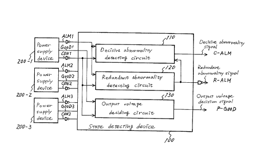
Referring to Fig. 1, a power supply system includes a
plurality of power supply devices 200-1, 200-2 and 200-3, and
a state detecting device 100 connected with the plurality of
power supply devices 200-l, 200-2 and 200-3. Each of the
plurality of power supply devices 200-1, 200-2 and 200-3
enables Hot Swap which signifies at least one of the power
supply devices is exchanged during power supply operation
without stoping the power supply system. Each of the power
supply devices outputs a connection state signal CONn*
(hereinafter, n is an integer number more than 0 representative
of number of the power supply device, and a symbol * means that
a transistor-transistor logic (TTL) level is "L" in a
significant state), an output voltage decision signal GOODn and
a power supply abnormality signal ALMn* to the state detecting
circuit 100. The connection state signal CONn* indicates that
the correspond power supply device is mounted on an appropriate
mount place where it should be mounted when it is "L" in the
TTL level. The output voltage decision signal GOODn indicates
that an output voltage value of a subject power supply device
is normal when it is "H" in the TTL level, which is the
significant state. The power supply abnormality signal ALMn*
- 5 -
,_ CA 02225972 1998-O1-15
indicates that the abnormality occurs in the subject power
supply device.
The state detecting circuit 100 includes a decisive
abnormality detecting circuit 110, a redundant abnormality
detecting circuit 120 and an output voltage deciding circuit
130. The decisive abnormality detecting circuit 110 detects
whether the plurality of power supply devices 200-1 to 200-3
are in a decisive abnormal state or not, that is, the power
supply devices required at the minimum in the structure of the
power supply system are in an abnormal state or not, according
to a detection result from the redundant abnormality detecting
circuit 120, the power supply abnormality signal ALMn*outputted
from the respective power supply devices 200-1, 200-2 and 200-3
and the connection state signal CONn* outputted from the
respective power supply devices 200-1, 200-2 and 200-3. The
redundant abnormality detecting circuit 120 detects whether a
redundant power device of the plural power supply devices 200-
1, 200-2 and 200-3 are in an abnormal state or not, according
to the power supply abnormality signal ALMn* and the connection
state signal CONn* outputted from the respective power supply
devices 200-1, 200-2 and 200-3, respectively. The output
voltage deciding circuit 130 detects whether the plural power
supply devices 200-1, 200-2 and 200-3 output a normal voltage
or not, according to the output voltage decision signal GOODn
and the connection state signal CONn* outputted from the plural
power supply devices 200-1, 200-2 and 200-3, respectively.
Referring to Fig. 2, the decisive abnormality detecting
circuit 110 includes two-input NAND gates 111, 112 and 113 that
output a signal indicating whether the respective power supply
- 6 -
CA 02225972 1998-O1-15
devices as mounted are in the abnormal state or not, a two-
input NAND gate 114 that outputs a signal indicating whether at
least one abnormal power supply device exists in the respective
power supply devices as mounted or not, and a two-input AND
gate 115 that outputs a decisive abnormality signal C-ALM in
accordance with a signal outputted from the two-input NAND gate
114 and a signal outputted from the redundant abnormality
detecting circuit 120. The decisive abnormality signal C-ALM
indicates that abnormality occurs even in non-redundant power
supply devices which are an essential power supply devices in
the structure of the power supply system among the plural power
supply devices. The power supply abnormality signals ALMl*,
ALM2* and ALM3* are inputted to each one input terminal of the
two-input NAND gates 111, 112 and 113 through an inverter gate,
respectively. The input signal CON1* is inputted to the other
input terminal of the two-input NAND gate 111 through the
inverter gate. The input signal CON2* is inputted to the other
input terminal of the two-input NAND gate 112 through the
inverter gate. The input signal CON3* is inputted to the other
input terminal of the two-input NAND gate 113 through the
inverter gate. The output terminal of the two-input NAND gate
111 is connected to a first input terminal of the three-input
NAND gate 114. The output terminal of the two-input NAND gate
112 is connected to a second input terminal of the three-input
NAND gate 114. The output terminal of the two-input NAND gate
113 is connected to a third input terminal of the three-input
NAND gate 114. An output terminal of the three-input NAND gate
114 is connected to one input terminal of the two-input AND
gate 115. The other input terminal of the two-input AND gate
CA 02225972 1998-O1-15
115 is connected with the output of the redundant abnormality
detecting circuit 120. From the output terminal of the two-
input AND gate 115, the decisive abnormality signal C-ALM is
outputted as the significant state "H" in the TTL level of .
Referring to Fig. 3, the redundant abnormality
detecting circuit 120 includes two-input NAND gates 121, 122
and 123 that output a signal indicating that the respective
power supply devices as mounted are abnormal or not, a three-
input NAND gate 124 that outputs a signal indicating whether a
redundant power supply device is included in the plurality of
power supply devices or not, a decoder 125, and a three-input
AND gate 126 which output a redundant abnormality signal R-ALM
indicating whether the abnormality occurs in the redundant
power supply device when the redundant power supply devices is
connected to the power supply system. The power supply
abnormality signals ALMl*, ALM2* and ALM3* are inputted to each
one input terminals of the two-input NAND gates 121, 122 and
123 through an inverter gate, respectively. The input signal
CON1* is connected to the other input terminal of the two-input
NAND gate 121 and also connected to a first input terminal of
the three-input NAND gate 124, through an inverter gate. The
input signal CON2* is connected to the other input terminal of
the two-input NAND gate 122 and also connected to a second
input terminal of the three-input NAND gate 124, through an
inverter gate. The input signal CON3* is connected to the
other input terminal of the two-input NAND gate 123 and also
connected to a third input terminal of the three-input NAND
gate 124, through an inverter gate. An output terminal of the
two-input NAND gate 121 is connected to a select A terminal of
_ g _
- , CA 02225972 1998-O1-15
the decoder 125. An output terminal of the two-input NAND gate
122 is connected to a select B terminal of the decoder 125. An
output terminal of the two-input NAND gate 123 is connected to
a select C terminal of the decoder 125. An output terminal of
the three-input NAND gate 124 is connected to enable terminals
G2A and G2B of the decoder 125. The "H" level of TTL is always
applied to the enable terminal G1 of the decoder 125. Output
terminals Y3, Y5 and Y6 of the decoder 125 are connected to the
first, second and third input terminals of the three-input AND
gate 126, respectively.
Fig. 6 shows a relation between an input signal and an
output signal of the decoder 125. For example, it may be used
a 3-to-8 line decoder as the decoder 125.
Again referring to Fig. 3, from the output terminal of
the three-input AND gate 126, the redundant abnormality signal
R-ALM is outputted as the TTL level "H" through the inverter
gate. Further, the output of the three-input AND gate 126 is
also supplied to the other input terminal of the two-input AND
gate 115.
Referring to Fig. 4, the output voltage deciding
circuit 130 includes two-input NAND gates 131, 132 and 133 that
output a signal indicating whether an output voltage value
outputted from the respective power supply devices as mounted
is normal or not, and a three-input NAND gate 134 that detects
whether at least one of the power supply devices which outputs
a normal output voltage value exists in the plurality of power
supply devices or not, and that outputs an output voltage
decision signal P-GOOD indicating that the output voltage value
of the power supply system is normal when at least one power
- 9 -
CA 02225972 1998-O1-15
supply device outputting the normal output voltage value
exists. The output voltage decision signals GOODl, GOOD2 and
GOOD3 are connected to each of one input terminals of the two-
input NAND gates 131, 132 and 133, respectively. The input
signal CON1* is inputted to the other input terminal of the
two-input NAND gate 131 through an inverter gate. The input
signal CON2* is connected to the other input terminal of the
two-input NAND gate 132 through an inverter gate. The input
signal CON3* is connected to the other input terminal of the
two-input NAND gate 133 through an inverter gate. The output
terminals of the two-input NAND gates 131, 132 and 133 are
inputted to the first, second and third input terminals of the
three-input NAND gate 134, respectively. From the output
terminal of the three-input NAND gate 134, the output voltage
decision signal P-GOOD is outputted as the TTL level "H" which
indicates significant state.
Then, an operation of this embodiment are described
below.
Referring to Figs. 3 and 5, in the non-redundant
operation mode, that is, in the case where only two power
supply devices operate in parallel, the power supply system is
made up of the power supply devices 200-1 and 200-2.
In Figs. 3, 5 and 6, because the power supply device
200-3 is not connected to the state detecting device 100, the
connection state signal CON3* of the power supply device 200-3
is always "H" in TTL level, and the input signals inputted to
the enable terminals G2A and G2B of the decoder 125 in the
redundant abnormality detecting circuit 120 are always "H" in
TTL level. As a result all of the output terminals Y3, Y5 and
- 10 -
CA 02225972 1998-O1-15
Y6 of the decoder 125 are "H" in TTL level, and then, the
redundant abnormality signal R-ALM outputted from the redundant
abnormality detecting circuit 120 through the inverter gate
becomes "L" in TTL level which represents a normal state.
Referring to Figs. 2 and 5, when the power supply
devices 200-1 and 200-2 normally operate, their power supply
abnormality signals ALM1* and ALM2* are "H" in TTL level, and
the decisive abnormality signal C-ALM outputted through the
two-input AND gate 115 of the decisive abnormality detecting
circuit 110 is "L" in TTL level which represents the normal
state.
In Figs. 4 and 5, when the power supply devices 200-1
and 200-2 normally operate, the output voltage decision signals
GOOD1 and GOOD2 outputted from those devices are "H" in TTL
level, and the output voltage decision signal P-GOOD outputted
through the three-input NAND gate 134 of the output voltage
deciding circuit 130 is "H" in TTL level which represents the
normal operation state.
Referring to Figs. 2 and 5, when abnormality occurs in
the power supply device 200-1 in the above state, for example,
the power supply abnormality signal ALM1* of the power supply
device 200-1 becomes "L" in TTL level. Therefore, the decisive
abnormality signal C-ALM outputted through the two-input AND
gate 115 of the decisive abnormality detecting circuit 110
changes to "H" in the TTL level which represents the decisive
abnormal state.
Next, an operation of the power supply system in the
redundant operation mode are described hereinafter. In the
redundant operation mode, three power supply devices operate in
- 11 -
CA 02225972 1998-O1-15
parallel, the power supply system is made up of the power
supply devices 200-1, 200-2 and 200-3.
Referring to Figs. 2 and 5, when the power supply
devices 200-1, 200-2 and 200-3 normally operate, the power
supply abnormality signals ALM1* , ALM2* and ALM3* outputted
from those devices are "H" in TTL level, and the decisive
abnormality signal C-ALM outputted through the two-input AND
gate 115 of the decisive abnormality detecting circuit 110 is
"L" in TTL level which represents the normal state.
In Figs. 3, 5 and 6, since all of the connection state
signals CON1*, CON2* and CON3* of the power supply devices 200-
1, 200-2 and 200-3, respectively, are "L" in TTL level, the
input signals inputted to the enable terminals G2A and G2B of
the decoder 125 in the redundant abnormality detecting circuit
120 are always "L" in TTL level. Further, because the power
supply abnormality signals ALM1*, ALM2* and ALM3* of the power
supply devices 200-1, 200-2 and 200-3, respectively, are "H" in
TTL level, the level "H" of TTL is inputted to the select
terminals A, B and C of the decoder 125 in the redundant
abnormality detecting circuit 120, respectively. As a result,
all of the output terminals Y3, Y5 and Y6 of the decoder 125
become "H" in TTL level, and the redundant abnormality signal
R-ALM outputted through the inverter gate becomes "L" in TTL
level which represents that the abnormality does not occur in
the redundant power supply device.
Referring to Figs. 4 and 5, when the power supply
devices 200-1, 200-2 and 200-3 normally operate, the output
voltage decision signals GOOD1, GOOD2 and GOOD3 outputted from
those devices are "H" in TTL level, and the output voltage
- 12 -
CA 02225972 1998-O1-15
decision signal P-GOOD outputted from the three-input NAND gate
134 of the output voltage deciding circuit 130 is "H" in TTL
level which represents that the output voltage value of the
power supply system is normal.
Then, an operation of the power supply system in a case
where abnormality occurs in at least one of the power supply
devices while the power supply system is operating in the
redundant operation mode.
In Figs. 3, 5 and 6, when abnormality occurs in the
power supply device 200-1, for example, the power supply
abnormality signal ALM1* outputted from the power supply device
200-1 becomes "L" in TTL level. As a result, in the redundant
abnormality detecting circuit 120, only the select terminal A
of the select terminals A, B and C of the decoder 125 becomes
"L" in TTL level, and then, the output terminal Y6 of the
decoder 125 becomes "L" in TTL level. The signal "L" in TTL
level outputted from the output terminal Y6 of the decoder 125
in the redundant abnormality detecting circuit 120 is inputted
to the third input terminal of the three-input AND gate 126,
and the output terminal of the three-input AND gate 126 becomes
"L" in TTL level. For that reason, the redundant abnormality
signal R-ALM outputted through a driver gate from the redundant
abnormality detecting circuit 120 becomes "H" in TTL level
which represents that the abnormality occurs in at least one of
the redundant power supply devices. The signal "L" in TTL
level outputted from the output terminal of the three-input AND
gate 126 of the redundant abnormality detecting circuit 120 is
inputted to the other input terminal of the two-input AND gate
115 in the decisive abnormality detecting circuit 110.
- 13 -
CA 02225972 1998-O1-15
Referring to Figs. 2 and 5, in the decisive abnormality
detecting circuit 110, the signal ALM1* "L" in TTL level is
inputted from the power supply device 200-1 in which
abnormality occurs to one input terminal of the two-input NAND
gate 111 through the inverter gate. Since the power supply
device 200-1 in which abnormality occurs is still connected to
the power supply system, the signal CONl* "L" in TTL level
outputted from the power supply device 200-1 is inputted to the
other input terminal of the two-input NAND gate 111 through the
inverter gate. For this reason, from the output terminal of
the two-input NAND gate 111, the output signal "L" in TTL level
which represents that abnormality occurs in the power supply
device 200-1 as mounted is inputted to the three-input NAND
gate 114. The three-input NAND gate 114 outputs "H" in TTL
level to one input terminal of the two-input AND gate 115.
Since the signal "L" in TTL level outputted from the three-
input AND gate 126 of the redundant abnormality detecting
circuit 120 is inputted to the other input terminal of the two-
input AND gate 115, the two-input AND gate 115 outputs the
decisive abnormality signal C-ALM whose value is "L" in TTL
level representing that the power supply system is not in the
decisive abnormal state.
In this way, even if abnormality occurs in redundancy
of the power supply devices, because the redundant abnormality
signal R-ALM exhibits that the redundant power supply device is
merely abnormal, and because the decisive abnormality signal C-
ALM does not exhibit the abnormality, it can be recognized from
the outside of the power supply system that only the redundancy
is abnormal among the power supply devices, and also the power
- 14 -
CA 02225972 1998-O1-15
supply system can operate without stopping the power supply
system per se.
Next, an operation of the power supply system in a case
where further abnormality occurs even in the power supply
device 200-2 in addition to the power supply device 200-1 will
be described.
Referring to Figs. 5 and 6, in the redundant
abnormality detecting circuit 120, when abnormality occurs in
the power supply device 200-2, the power supply abnormality
signal ALM2* outputted from the power supply device 200-2
becomes "L" in TTL level. For that reason, not only the select
terminal A of the decoder 125 but also the signal inputted to
the select terminal B become "L" in TTL level, and all of the
output terminals Y3, Y5 and Y6 of the decoder 125 output "H" in
TTL level. As a result, the output of the three-input AND gate
126 becomes "H" in TTL level, and then, the redundant
abnormality signal R-ALM outputted through the inverter gate
becomes "L" in TTL level which represents that it is not in the
redundant abnormal state.
Referring to Figs. 2 and 5, the output signal from the
output terminal of the three-input AND gate 126 which is
inputted to the other input terminal of the two-input AND gate
115 changes to "H" in TTL level. Further, in the decisive
abnormality detecting circuit 110, since the signal "H" in TTL
level which represents that abnormality occurs in at least one
of the mounted power supply devices is inputted to one input
terminal of the two-input AND gate 115 from the three-input
NAND gate 114, the decisive abnormality signal C-ALM outputted
from the output terminal of the two-input AND gate 115 becomes
- 15 -
CA 02225972 1998-O1-15
"H" in TTL level which represents that it is in the decisive
abnormal state.
In this way, in this embodiment, because the decisive
abnormality detecting circuit 110 outputs the decisive
abnormality signal C-ALM only when the number of the abnormal
power supply devices exceeds the number of the redundant power
supply devices, the abnormality can be distinguished between a
abnormality which does not need to stop the power supply system
and the decisive abnormality which needs to stop the power
supply system.
Then, a second embodiment of the present invention is
described below in detail, referring to the drawings. In case
of the redundant operation mode, the state detecting device 100
of the power supply system, according to the above-described
first embodiment, outputs the redundant abnormality signal when
the abnormality occurs in one power supply device. When the
abnormal power supply device is replaced by a normal one by Hot
Swap for maintenance, however, the redundant abnormality
signal is canceled by extracting the abnormal power supply
device as follows:
In Fig. 7, when abnormality occurs in the power supply
device 200-1, because the power supply abnormality signal ALM1*
and the connection state signal CON1* which are outputted from
the power supply device 200-1 is "L" in TTL level, the
redundant abnormality signal R-ALM becomes "H" in TTL level
which represents that the power supply system is in the
redundant abnormal state. Then, when the power supply device
200-1 is extracted from the power supply system by Hot Swap,
the power supply abnormality signal ALM1* inputted to the state
- 16 -
CA 02225972 1998-O1-15
detecting circuit 100 changes from "L" to "H" in TTL level.
This is because the power supply abnormality signal ALMn* is
pulled up to become "H" in TTL level when a corresponding power
supply device is not connected to the power supply system,
6 whereby the power supply system can operate in any one of the
non-redundant operation mode or the redundant operation mode.
At the same time, since the power supply device 200-1 is not
mounted on the power supply system, the connection state signal
CON1* changes from "L" to "H" in TTL level. In this manner, in
the redundant abnormality detecting circuit 120, because the
power supply abnormality signal ALMl* and the connection state
signal CON1* change, the terminal A of the decoder 125 changes
from "L" to "H" in TTL level, and all of the output terminals
Y3, Y5 and Y6 of the decoder 125 become "H" in TTL level. For
that reason, the redundant abnormality signal R-ALM outputted
through the inverter gate becomes "L" in TTL level which
represents that the power supply system is not in the redundant
abnormal state. Therefore, a host monitor device (not shown)
monitoring the redundant abnormal state monitors as if the
redundant abnormality signal R-ALM has not asserted.
The feature of the second embodiment resides in that
the power supply system includes a holding circuit 400 that
holds the redundant abnormality signal R-ALM for a
predetermined time, and an updating circuit 300 that resets the
redundant abnormality signal R-ALM after a lapse of the
predetermined time for which the holding circuit 400 holds the
redundant abnormality signal R-ALM.
Referring to Fig. 8, the updating circuit 300 includes
one-shot circuits 321, 322 and 323 each of which is provided
- 17 -
CA 02225972 1998-O1-15
for each of a plurality of the power supply devices 200-1, 200-
2 and 200-3 to output a fine-width pulse, and timer circuits
311, 312 and 313 each of which is provided for each of a
plurality of the power supply devices 200-1, 200-2 and 200-3 to
prevent the holding circuit 400 from being reset by a chatter
in case of Hot Swap. The power supply abnormality signals
ALM1*, ALM2* and ALM3* outputted from the plurality of power
supply devices 200-l, 200-2 and 200-3 are inputted to one input
terminals of the timer circuits 311, 312 and 313, respectively.
The output voltage decision signals GOOD1, GOOD2 and GOODS
outputted from the plurality of power supply devices 200-l,
200-2 and 200-3 are inputted to the respective one-shot
circuits 321, 322 and 323, respectively. The connection state
signals CONl*, CON2* and CON3* outputted from the plurality of
power supply devices 200-1, 200-2 and 200-3 are inputted to the
other input terminals of the timer circuits 311, 312 and 313
through the inverter gates, respectively. The output terminal
of the one-shot circuit 321 and the output terminal of the
timer circuit 311 are connected to one input terminal and the
other input terminal of the two-input NAND gate 331,
respectively. The output terminal of the one-shot circuit 322
and the output terminal of the timer circuit 312 are connected
to one input terminal and the other input terminal of the two-
input NAND gate 332, respectively. The output terminal of the
one-shot circuit 323 and the output terminal of the timer
circuit 313 are connected to one input terminal and the other
input terminal of the two-input NAND gate 333, respectively.
The output terminals of the two-input NAND gates 331, 332 and
333 are connected to the first, second and third input
- 18 -
CA 02225972 1998-01-15
terminals of the three-input AND gate 341, respectively. The
output terminal of the three-input AND gate 341 is connected to
the holding circuit 400. The holding circuit 400 includes two-
input NAND gates 401 and 402. One input terminal of the two-
s input NAND gate 401 receives the output signal from the
redundant abnormality detecting circuit 120 of the state
detecting circuit 100. The other input terminal of the two-
input NAND gate 401 receives the output of the two-input NAND
gate 402. From the output terminal of the two-input NAND gate
401, the redundant abnormality signal R-ALM is outputted. One
input terminal of the two-input NAND gate 402 receives a signal
outputted from the updating circuit 300. The other input
terminal of the two-input NAND gate 402 receives the output of
the two-input NAND gate 401.
Referring to Fig. 9, the timer circuit 311 includes
resistors R1, R2, R3, R4, R5, R6, R7 and R8, a two-input HAND
gate 3111, a transistor 3112, a capacitor C1, a comparator
3113, and a driver gate 3114. The power supply abnormality
signal ALMl* and the connection state signal CON1* are inputted
to the two-input NAND gate 3111. The output of the two-input
NAND gate 3111 is connected to the base terminal of the
transistor 3112 and one end of the resistor R2 through the
resistor R1. The other end of the resistor R2 is connected to
the ground potential. The collector terminal of the transistor
3112 is connected to VCC through the resistor R3 and connected
to one end of the resistor R4, and the emitter terminal of the
transistor 3112 is connected to the ground potential. The
other end of the resistor R4 is connected to one end of the
capacitor C1 and also connected to an inverting input terminal
- 19 -
CA 02225972 1998-O1-15
of the comparator 3113. The other end of the capacitor C1 is
connected to the ground potential. A non-inverting input
terminal of the comparator 3113 is connected to the power
supply VCC through the R5 and also connected to the ground
potential through the resistor R6. An output signal of the
comparator 3113 is outputted through the driver gate 3114 as an
output signal of the timer circuit 311. Also, the output of
the comparator 3113 is connected to the power supply VCC
through the resistor R8 and also connected to a second input of
the comparator 3113 through the resistor R7. The same
structure is applied to the circuit structure of other timer
circuits 312 and 313.
Referring to Fig. 10, the timer circuits 311, 312 and
313 output an output signal "H" in TTL level as the significant
state after a lapse of predetermined time T1 since the inverse
levels of two input signals, that is, the power supply
abnormality signal ALMn* and the connection state signal CONn*
become "H" in TTL level. The symbol M is a waveform at a
middle point of Fig. 9.
Referring to Fig. 11, the one-shot circuit 321 includes
an inverter 3211, resistors r1 and r2, a capacitor C2 and an
AND gate 3212. The output voltage decision signal GOOD1
inputted to the one-shot circuit 321 is inputted to the
inverter 3211 and the first input terminals of the AND gate
3212. The output of the inverter 3211 is connected to the
power supply VCC through the resistor rl and also inputted to
the second input terminal of the AND gate 3212 through the
resistor r2. The second input terminal of the AND gate 3212 is
connected to the ground potential through the capacitor C2.
- 20 -
CA 02225972 1998-O1-15
The same circuit structure is applied to the one-shot circuits
322 and 323.
Referring to Fig. 12, the respective one-shot circuits
321, 322 and 323 output a pulse signal "H" as the significant
state in TTL level for a second predetermined time T2 every
time the input signal, that is, the output voltage decision
signal GOODn changes from "L" to "H" in TTL level. The symbol
m is a waveform at a middle point of Fig. 11.
Next, an operation of this embodiment is described
below.
Referring to Figs. 8 and 13, in a case where
abnormality occurs in the power supply device 200-1, the power
supply device 200-1 is replaced by a normal one by Hot Swap.
In accordance with the abnormality in the power supply device
200-1, the power supply abnormality signal ALM1* and the
connection state signal CON1* outputted from the power supply
device 200-1 change to "L" in TTL level, and then, a signal
outputted from the redundant abnormality detecting circuit 120
becomes "H" in TTL level which represents the redundancy is
merely in abnormality state. When the power supply device 200-
1 is extracted from the power supply system Hot Swap, the power
supply abnormality signal ALM1* and the connection state signal
CON1* change from "L" to "H" in TTL level. As a result, the
terminal A of the decoder 125 changes from "L" to "H" in TTL
level, and all of the output terminals Y3, Y5 and Y6 of the
decoder 125 become "H" in TTL level. In this manner, the
output of the three-input AND gate 126 changes from "H" in TTL
level which represents that the power supply system is in the
redundant abnormality state to "L" in TTL level which
- 21 -
CA 02225972 1998-O1-15
represents that the power supply system is not in the redundant
abnormality state. However, the holding circuit 400 holds the
signal outputted from the redundant abnormality detecting
circuit 120 as "H" in TTL level which represents the redundancy
is in the abnormality state. Then, the normal power supply
device is inserted in the mount place of the power supply
device 200-1 as a alternative by Hot Swap. The connection
state signal CON1* changes from an unsettled TTL level or the
TTL level "H" which represents that the power supply device
200-1 is not connected to the power supply system to the TTL
level "L" which represents that the power supply device 200-1
is connected to the power supply system. The power supply
abnormality signal ALMl* settles from an unsettled TTL level or
the TTL level "H" which represents that the power supply system
is not abnormal to "H" in TTL level which represents that it is
not abnormal. The output voltage decision signal GOOD1 changes
from an unsettled TTL level or the TTL level "L" which
represents that the output voltage value is not normal to "H"
in TTL level which represents that the output voltage value is
normal after a lapse of a predetermined time since a power
supply turn-on signal not shown is inputted to the power supply
device 200-1. The one-shot circuit 321 outputs a narrow width
pulse at a timing when the output voltage decision signal GOODl
changes to "H" in TTL level. The pulse outputted from the one-
shot circuit 321 is inputted to the holding circuit 400 to
reset the signal outputted from the redundant abnormality
detecting circuit 120 held by the holding circuit 400.
The power supply device 200-1 is connected to the power
supply system through physical connection due to contact of a
- 22 -
CA 02225972 1998-O1-15
connector or the like. For this reason, in the case where the
power supply device 200-1 is inserted by Hot Swap, the chatter
of several millisecond to several dozens of millisecond
duration may occur in the respective signals of the connection
state signal CONl*, the power supply abnormality signal ALM1*
and the output voltage decision signal GOOD1, or the connection
order of the respective signals may get unfixed. In the
updating circuit 300, when the output voltage decision signal
GOOD1 is chattered, the one-shot circuit 321 outputs a pulse.
The timer circuits 311, 312 and 313 prevent the pulse which the
one-shot circuit 321 outputs from resetting the redundant
abnormality signal R-ALM. As a result, the predetermined time
T1 of the timer circuits 311, 312 and 313 is set such that it
becomes sufficiently longer than a time which the chatter is
arising when the power supply device 200-1 is inserted to the
power supply system. On the other hand, the predetermined time
T1 is set so as not to exceed a time from the power supply
turn-on signal is inputted to the power supply device 200-1 to
the connection state signal CON1 is fixed to the TTL level "H".
More particularly, it is desirable that the predetermined time
T1 is 100 to 200 millisecond. Moreover, the predetermined time
T2 of the pulse outputted from the one-shot circuits 321, 322
and 323 is set such that it becomes sufficiently longer than
the reset time of the holding circuit 400. More particularly,
it is preferable that the predetermined time T2 is 1 to 2
millisecond.
As described above, in this embodiment, even if the
signal outputted from the redundant abnormality detecting
circuit 120 is canceled when the abnormal power supply device
- 23 -
CA 02225972 1998-O1-15
200-1 is extracted from the power supply system by Hot Swap,
because the holding circuit 400 holds the signal outputted from
the redundant abnormality detecting circuit 120, the redundant
abnormality signal R-ALM is prevented from being canceled.
Further, in this embodiment, the power supply system is
designed in such a manner that the timer circuits 311, 312 and
313 are provided, and the holding circuit 400 is reset first
when the output voltage value of the power supply device 200-1
becomes normal after the power supply device 200-1 is inserted
into the power supply system. With this structure, the
redundant abnormality signal R-ALM can be prevented from being
reset by the chatter when the power supply device 200-1 which
has been replaced by a normal one is inserted into the power
supply system by Hot Swap.
In the above embodiment, while the decoder 125 is
provided in the redundant abnormality detecting circuit 120,
the present invention is not limited by or to this structure.
It is possible to use any logic circuit that can output a
signal representing whether abnormality occurs in the redundant
power supply device or not. Moreover, in the above-mentioned
embodiments, while the circuit is formed by the TTL circuit,
the TTL circuits may be replaced by emitter coupled logic (ECL)
circuits or complementary metal oxide semiconductor (CMOS)
circuits.
While this invention has been described in conjunction
with the preferred embodiments thereof, it will now readily be
possible for those skilled in the art to put this application
into practice in various other manners.
- 24 -